 | ÐлекÑÑоннÑй компоненÑ: 74LVC1284 | СкаÑаÑÑ:  PDF PDF  ZIP ZIP |
Äîêóìåíòàöèÿ è îïèñàíèÿ www.docs.chipfind.ru
Philips
Semiconductors
74LVC1284
3.3V Parallel printer interface
transceiver/buffer
Product specification
1995 Nov 10
INTEGRATED CIRCUITS
IC24 Low Voltage Handbook
Philips Semiconductors
Product specification
74LVC1284
3.3V Parallel printer interface transceiver/buffer
2
1995 Nov 10
853-1819 16000
FEATURES
·
Asynchronous operation
·
4-Bit transceivers
·
3 additional buffer/driver lines
·
TTL compatible inputs
·
ESD protection exceeds 1000V per MIL STD 883 Method 3015
and 200V per Machine Model
·
Input Hysteresis
·
Low Noise Operation
·
Center Pin V
CC
& GND
·
IEEE 1284 Compliant Level 1 & 2
·
Overvoltage Protection on B side
DESCRIPTION
The 74LVC1284 parallel interface chip is designed to provide an
asynchronous, 4-bit, bi-directional, parallel printer interface for
personal computers. Three additional lines are included to provide
handshaking signals between the host and the peripheral. The part
is designed to match IEEE 1284 standard.
The 4 transceiver pins (A/B 1-4) allow data transmission from the A
bus to the B bus, or from the B bus to the A bus, depending on the
state of the direction pin DIR.
The B bus and the Y5-Y7 lines have totem pole or open drain style
outputs depending on the state of the high drive enable pin HD.
The A bus only has totem pole style outputs. All inputs are TTL
compatible with at least 300mV of input hysteresis at V
CC
= 3.3V.
QUICK REFERENCE DATA
SYMBOL
PARAMETER
CONDITIONS
T
amb
= 25
°
C; GND = 0V
TYPICAL
UNIT
R
D
B/Y Side output resistance
V
CC
= 3.3V; V
O
= 1.65V
"
0.2V (See Figure 2)
45
SR
B/Y Side slew rate
R
L
= 62
; C
L
= 50pF (See Waveform 4)
0.2
V/ns
I
CC
Total static current
V
I
= V
CC
/GND; I
O
= 0
5
µ
A
V
HYS
Input hysteresis
V
CC
= 3.3V
0.4
V
t
PLH
/t
PHL
A B/Y
Propagation delay
to the B/Y side outputs
V
CC
= 3.3V
12.6/12.4
ns
ORDERING INFORMATION
PACKAGES
TEMPERATURE RANGE
ORDER CODE
DRAWING NUMBER
20-pin plastic SO
0
°
C to +70
°
C
7LVC1284 D
SOT163-1
20-pin plastic SSOP Type II
0
°
C to +70
°
C
74LVC1284 DB
SOT339-1
20-pin plastic TSSOP Type I
0
°
C to +70
°
C
74LVC1284 PW
SOT360-1
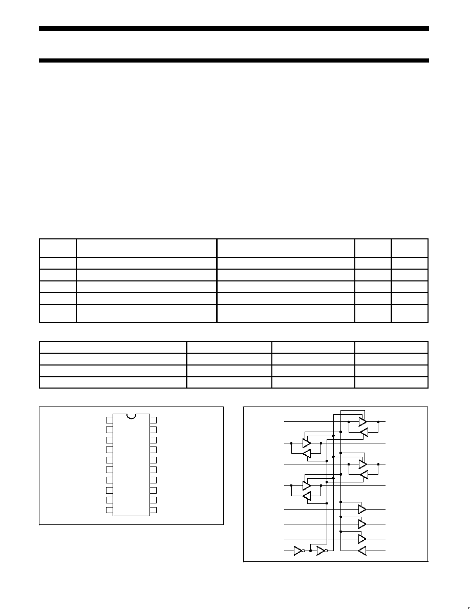
PIN CONFIGURATION
1
2
3
4
5
6
7
8
9
10
11
12
13
14
15
16
17
18
19
20
A1
A2
A3
A4
GND
GND
A5
A6
A7
DIR
B1
B2
B3
B4
V
CC
V
CC
Y5
Y7
Y6
HD
SK00001
LOGIC SYMBOL
DIR
HD
Y7
A7
A
Y
Y6
A6
A
Y
Y5
A5
A
Y
B4
A4
A
B
A
B
B2
A2
A
B
A
B
B3
A3
B1
A1
SK00009
Philips Semiconductors
Product specification
74LVC1284
3.3V Parallel printer interface transceiver/buffer
1995 Nov 10
3
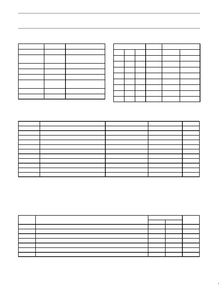
PIN DESCRIPTION
PIN NUMBER
SYMBOL
FUNCTION
1,2,3,4
A1 - A4
Data inputs/outputs
20,19,18,17
B1 - B4
IEEE 1284 Std.
outputs/inputs
7,8,9
A5 - A7
Data inputs
14,13,12
Y5 - Y7
IEEE 1284 Std. outputs
10
DIR
Direction selection
11
HD
B/Yside high drive
enable/disable
5,6
GND
Ground (0V)
15,16
V
CC
Positive supply voltage
FUNCTION TABLE
INPUTS
OUTPUTS
INPUTS/OUTPUTS
DIR
HD
A5-7
Y5-7
A1-4
B1-4
L
L
L
L
A = B
Inputs
L
L
H
Z
A = B
Inputs
L
H
L
L
A = B
Inputs
L
H
H
H
A = B
Inputs
H
L
L
L
Inputs Low
Outputs Low
H
L
H
Z
Inputs High
Outputs Z
H
H
L
L
Inputs
B = A
H
H
H
H
Inputs
B = A
H = High Voltage
L = Low Voltage
Z = High Impedance, Off-State
ABSOLUTE MAXIMUM RATINGS
1, 2
SYMBOL
PARAMETER
CONDITIONS
RATING
UNIT
ESD Immunity, per Mil Std 883C method 3015
"
2
kV
V
CC
DC supply voltage
0.5 to +4.6
V
I
IK
DC input diode current
V
I
< 0
"
20
mA
I
OK
DC output diode current
V
O
< 0
"
50
mA
V
IN
DC input voltage
3
0.5 to +5.5
V
V
OUT
B/Y
DC
DC output voltage on B/Y side
3
0.5 to +5.5
V
V
OUT
B/Y (tr)
Transient output voltage on B/Y side
4
40ns transient
2 to +7
V
V
OUT
A side
DC output voltage on A side
0.5 to V
CC
+0.5
V
I
O
DC output current
Outputs in High or Low state
"
50
mA
T
stg
Storage temperature range
60 to +150
°
C
I
CC
/I
GND
Continuous current through V
CC
or GND
"
200
mA
NOTES:
1. Stresses beyond those listed may cause permanent damage to the device. These are stress ratings only and functional operation of the
device at these or any other conditions beyond those indicated under "recommended operating conditions" is not implied. Exposure to
absolute-maximum-rated conditions for extended periods may affect device reliability.
2. The performance capability of a high-performance integrated circuit in conjunction with its thermal environment can create junction
temperatures which are detrimental to reliability. The maximum junction temperature of this integrated circuit should not exceed 150
°
C.
3. The input and output voltage ratings may be exceeded if the input and output current ratings are observed.
4. V
OUT
B/Y (tr) guarantees only that this part will not be damaged by reflections in application so long as the voltage levels remain in the
specified range.
RECOMMENDED OPERATING CONDITIONS
SYMBOL
PARAMETER
LIMITS
UNIT
SYMBOL
PARAMETER
MIN
MAX
UNIT
V
CC
DC supply voltage
3.0
3.6
V
V
I
Input voltage
0
V
CC
V
V
OUT
B/Y output voltage
0.5
5.5
V
V
OUT
A side output voltage
0
V
CC
V
I
OH
B/Y side output current High
14
mA
I
OL
B/Y side output current Low
14
mA
T
amb
Operating free-air temperature range
0
+70
°
C
Philips Semiconductors
Product specification
74LVC1284
3.3V Parallel printer interface transceiver/buffer
1995 Nov 10
4
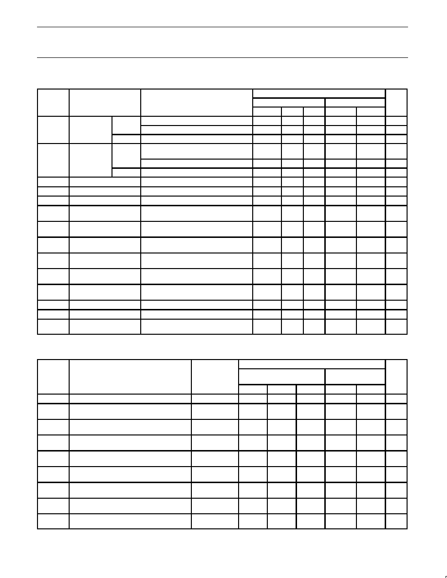
DC ELECTRICAL CHARACTERISTICS
LIMITS
SYMBOL
PARAMETER
TEST CONDITIONS
T
amb
= 25
°
C
T
amb
= 0
°
C to +70
°
C
UNIT
MIN
TYP
MAX
MIN
MAX
High level
An
V
CC
= Min to Max; I
OH
= 50
µ
A
V
CC
0.2
V
CC
V
CC
0.2
V
V
OH
High-level
output voltage
An
V
CC
= 3.0V; I
OH
= 4mA
2.4
2.4
V
out ut voltage
Bn or Yn
V
CC
= 3.0V; I
OH
= 14mA
2.2
2.4
2.1
V
V
Low-level
An
V
CC
= Min to Max; I
OL
= 50
µ
A;
V
I
= V
IL
or V
IH
0.2
0.2
V
V
OL
Low level
output voltage
V
CC
= 3.0V; I
OL
= 4mA; V
I
= V
IL
or V
IH
0.4
0.4
V
Bn or Yn
V
CC
= 3.0V; I
OL
= 14mA; V
I
= V
IL
or V
IH
0.8
0.9
V
V
IH
High-level input voltage
V
CC
= Min to Max
0.8
0.8
V
IL
Low-level input voltage
V
CC
= Min to Max
2.0
2.0
V
HYS
Input Hysteresis
V
CC
= 3.3V
0.4
0.3
V
R
D
B/Y side Output
Impedance
See Figure 2
38
45
53
35
55
I
I
Input leakage current
(A5-A7 DIR, HD)
V
CC
= 3.6V; V
O
= V
CC
or GND;
Not for I/O pins
±
1.0
±
5.0
µ
A
I
IHZ
/I
ILZ
Input current for common
I/O pins
V
CC
= 3.6V;V
I
= 5.5V or GND
"
0.1
"
15
µ
A
I
OFF
B/Y Side Power-off
leakage current
V
CC
= 0.0V; V
O
= 0 to 5.5V
±
10
±
100
µ
A
I
OZH
3-State output High
current Yn
V
CC
= 3.6V; V
O
= V
CC
; V
I
= V
IL
or V
IH
5
20
µ
A
I
OZL
3-State output Low
current Yn
V
CC
= 3.6V; V
O
= GND; V
I
= V
IL
or V
IH
5
20
µ
A
I
IH
+I
OZH
current
(A1 A4, Bn)
V
CC
= 3.6V; V
I/O
= V
CC
5
25
µ
A
I
IL
+I
OZL
current
(A1 A4, Bn)
V
CC
= 3.6V; V
I/O
= GND
5
25
µ
A
I
CC
Quiescent Supply
Current
V
CC
= 3.6V; I
O
= 0; V
I
= GND or V
CC
5
10
50
µ
A
AC CHARACTERISTICS
GND = 0V, t
R
= t
F
= 3.0ns, C
L
= 50pF, R
L
= 500
LIMITS
SYMBOL
PARAMETER
WAVEFORM
T
amb
= 25
°
C
V
CC
= 3.3V
T
amb
= 0 to + 70
°
C
V
CC
= Min to Max
UNIT
MIN
TYP
MAX
MIN
MAX
SR
B-Side Slew Rate
4
0.05
0.2
0.35
0.05
0.4
V/ns
t
PLH
t
PHL
Propagation delay
A toY or A to B
5
6.0
6.0
12.6
12.4
18.0
18.0
5.0
5.0
19.5
20.0
ns
t
PLH
t
PHL
Propagation delay
B to A
1
1.5
1.5
5.5
5.6
7.9
7.6
1.5
1.5
9.5
9.0
ns
t
PZH
t
PHZ
Output enable/disable time to/from High level
HD to Y or HD to B
2
4.0
2.0
12.0
6.5
16.0
9.1
4.0
2.0
20.0
11.0
ns
t
PZL
t
PLZ
Output enable/disable time to/from Low level
A to Y or A to B
2
5.0
1.5
12.7
5.0
16.3
7.1
5.0
1.5
20.0
9.0
ns
t
PZH
t
PZL
Output enable time
from DIR to B
2
8.0
8.0
12.3
12.7
18.0
18.0
4.0
4.0
20.0
20.0
ns
t
PHZ
t
PLZ
Output disable time
from DIR to B
2
5.0
6.0
8.9
9.1
12.5
12.0
2.0
2.0
14.5
14.0
ns
t
PZH
t
PZL
Output enable time
from DIR to A
2
3.5
4.0
6.9
8.6
13.0
14.0
3.0
3.0
14.5
16.0
ns
t
PHZ
t
PLZ
Output disable
from DIR to A
2
2.5
2.5
3.7
3.7
5.5
5.0
2.0
2.0
6.0
5.5
ns
Philips Semiconductors
Product specification
74LVC1284
3.3V Parallel printer interface transceiver/buffer
1995 Nov 10
5
AC WAVEFORMS
V
M
= 1.5V
V
X
= V
OL
"
0.3V
V
Y
= V
OH
0.3V
V
OL
and V
OH
are the typical output voltage drops that occur with the
output load. (V
CC
never goes below 3.0V).
V
M
t
PLH
t
PHL
V
OH
V
OL
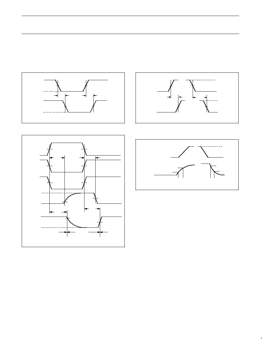
SY00001
V
M
INPUTS
GND
OUTPUTS
V = 2.7V
Waveform 1.
Input Bn to output An propagation delays
V
CC
OUTPUT
LOW-to-OFF
OFF-to-LOW
V
OL
V
OH
OUTPUT
HIGH-to-OFF
OFF-to-HIGH
GND
t
PZH
V
M
V
M
V
M
V
M
V
M
t
PZL
t
PHZ
t
PLZ
outputs
enabled
outputs
disabled
outputs
enabled
DIR
to A
DIR
to B
HD
to B
V
X
V
Y
SY00002
Waveform 2.
3-State enable and disable times
t
PLH
t
PHL
SY00008
INPUT
OUTPUT
2.4V
1.4V
0.4V
V
OUT
V
OUT
1.4V
1.4V
1.4V
Waveform 3.
Voltage Waveforms Propagation Delay Times
(A To B) Measured at Output Pin
0.4V
2.4V
0.9V
0.4V
t1
t2
t1
t2
2.4V
1.9V
INPUT
OUTPUT
SY00007
Waveform 4.
Slew Rate Waveforms Voltage Waveforms
(Input pulse rise and fall time are 3ns, 150ns
t
pulse width
t
10
µ
s,
for both a Low to High and a High to Low transition.)
Slew Rate measured between 0.4V and 0.9V - rising.
Slew Rate measured between 2.4V and 1.9V - falling.
Slew Rate measured at TP1.