Philips Semiconductors
Product specification
74LVC163
Presettable synchronous 4-bit binary counter;
synchronous reset
2
1998 May 20
853-1865 19421
FEATURES
∑
Wide supply voltage range of 1.2 V to 3.6 V
∑
In accordance with JEDEC standard no. 8≠1A
∑
Inputs accept voltages up to 5.5 V
∑
CMOS low power consumption
∑
Direct interface with TTL levels
∑
Synchronous reset
∑
Synchronous counting and loading
∑
Two count enable inputs for n≠bit cascading
∑
Positive edge≠triggered clock
DESCRIPTION
The 74LVC163 is a high-performance, low-power, low-voltage,
Si-gate CMOS device and superior to most advanced CMOS
compatible TTL families.
The 74LVC163 is a synchronous presettable binary counter which
features an internal look≠head carry and can be used for high-speed
counting. Synchronous operation is provided by having all flip-flops
clocked simultaneously on the positive-going edge of the clock (CP).
The outputs (Q
0
to Q
3
) of the counters may be preset to a HIGH or
LOW level. A LOW level at the parallel enable input (PE) disables
the counting action and causes the data at the data inputs
(D
0
to D
3
) to be loaded into the counter on the positive≠going edge
of the clock (provided that the set-up and hold time requirements for
PE are met). Preset takes place regardless of the levels at count
enable inputs (CEP and CET). A low level at the master reset input
(MR) sets all four outputs of the flip-flops (Q
0
to Q
3
) to LOW level
after the next positive-going transition on the clock (CP) input
(provided that the set-up and hold time requirements for PE are
met).
This action occurs regardless of the levels at CP, PE, CET and CEP
inputs This synchronous reset feature enables the designer to
modify the maximum count with only one external NAND gate.
The look≠ahead carry simplifies serial cascading of the counters.
Both count enable inputs (CEP and CET) must be HIGH to count.
The CET input is fed forward to enable the terminal count output
(TC). The TC output thus enabled will produce a HIGH output pulse
of a duration approximately equal to a HIGH level output of Q
0
. This
pulse can be used to enable the next cascaded stage. The
maximum clock frequency for the cascaded counters is determined
by the CP to TC propagation delay and CEP to CP set≠up time,
according to the following formula:
f
max
=
1
_______________________________
tp
(max)
(CP to TC) + t
SU
(CEP to CP)
QUICK REFERENCE DATA
GND = 0V; T
amb
= 25
∞
C; T
R
= T
F
2.5ns
SYMBOL
PARAMETER
CONDITIONS
TYPICAL
UNIT
t
PHL
/t
PLH
Propagation delay
CP to Q
n
CP to TC
CET to TC
C
L
= 50 pF
V
CC
= 3.3V
4.9
5.7
4.5
ns
f
MAX
maximum clock frequency
200
MHz
C
I
input capacitance
5.0
pF
C
PD
power dissipation capacitance per gate
notes 1 and 2
39
pF
NOTES:
1. C
PD
is used to determine the dynamic power dissipation (P
D
in
µ
W)
P
D
= C
PD
x V
CC
2
x f
i
+
(C
L
x V
CC
2
x f
o )
where:
f
i
= input frequency in MHz; C
L
= output load capacity in pF;
f
o
= output frequency in MHz; V
CC
= supply voltage in V;
(C
L
x V
CC
2
x f
o )
= sum of the outputs
2. The condition is V
1
= GND to V
CC
ORDERING INFORMATION
PACKAGES
TEMPERATURE RANGE
OUTSIDE NORTH AMERICA
NORTH AMERICA
DWG NUMBER
16-Pin Plastic SO
≠40
∞
C to +85
∞
C
74LVC163 D
74LVC163 D
SOT109-1
16-Pin Plastic SSOP Type II
≠40
∞
C to +85
∞
C
74LVC163 DB
74LVC163 DB
SOT338-1
16-Pin Plastic TSSOP Type I
≠40
∞
C to +85
∞
C
74LVC163 PW
74LVC163PW DH
SOT403-1
Philips Semiconductors
Product specification
74LVC163
Presettable synchronous 4-bit binary counter;
synchronous reset
1998 May 20
4
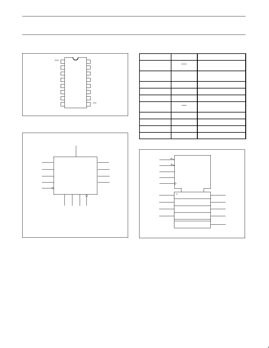
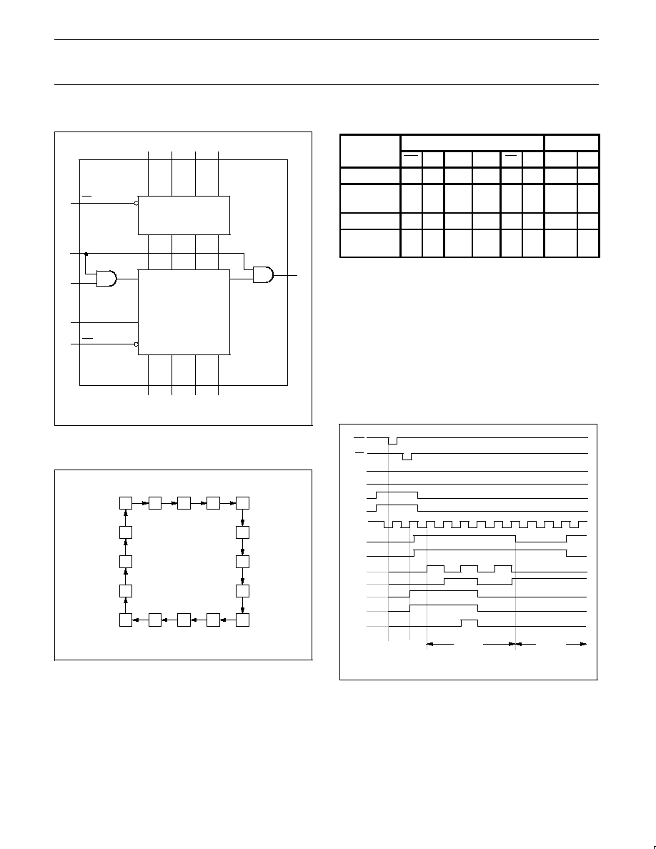
FUNCTIONAL DIAGRAM
PARALLEL LOAD
CIRCUITRY
BINARY
COUNTER
3
4
5
6
TC 15
14
13
12
11
Q
0
Q
1
Q
2
Q
3
1 MR
2
CP
7
D
0
D
1
D
2
D
3
CEP
CET
10
PE
9
SY00068
STATE DIAGRAM
8
7
6
5
4
12
11
10
9
13
14
15
0
1
2
3
SF00664
FUNCTION TABLE
OPERATING
INPUTS
OUTPUTS
MODES
MR
CP
CEP
CET
PE
Dn
Qn
TC
Reset (clear)
l
X
X
X
X
L
L
Parallel load
h
X
X
l
l
L
L
Parallel load
h
X
X
l
h
H
*
Count
h
h
h
h
X
count
*
Hold
h
X
l
X
h
X
q
n
*
(do nothing)
h
X
X
l
h
X
q
n
L
NOTES:
*
=
The TC output is High when CET is High and the counter
is at Terminal Count (HHHH)
H
=
High voltage level
h
=
High voltage level one setup time prior to the Low-to-High
clock transition
L
=
Low voltage level
l
=
Low voltage level one setup time prior to the Low-to-High
clock transition
q
=
Lower case letters indicate the state of the referenced
output one setup time prior to the Low-to-High clock
transition
X
=
Don't care
=
Low-to-High clock transition
TYPICAL TIMING SEQUENCE
CP
PE
TC
MR
INHIBIT
COUNT
CEP
CET
D0
D2
D1
D3
Q0
Q2
Q1
Q3
RESET PRESET
12
13
14
15
0
1
2
SY00069
Typical timing sequence: reset outputs to zero; preset to binary
twelve; count to thirteen, fourteen, fifteen, zero, one, and two;
inhibit