2004 Sep 07
2
Philips Semiconductors
Product specification
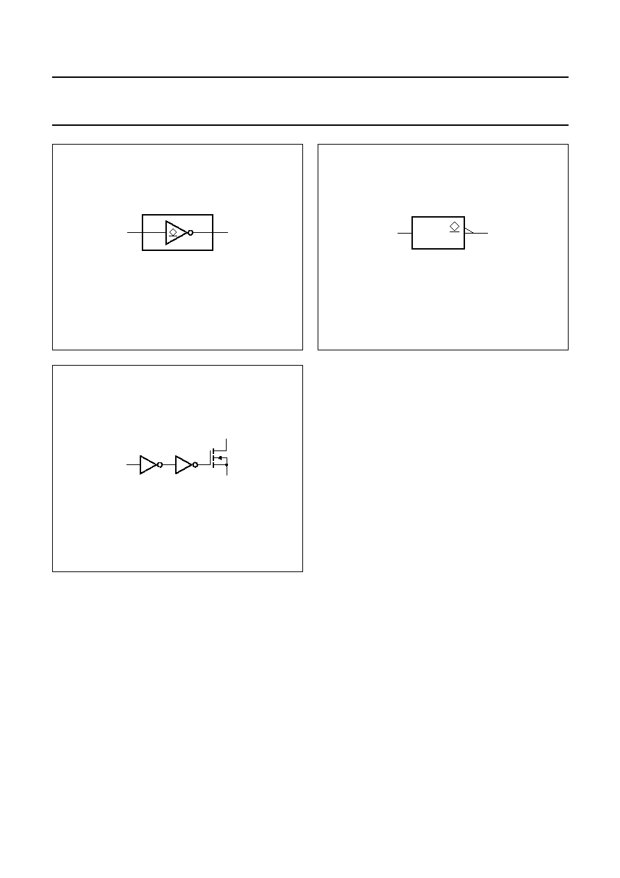
Inverter with open-drain output
74LVC1G06
FEATURES
∑
Wide supply voltage range from 1.65 to 5.5 V
∑
High noise immunity
∑
Complies with JEDEC standard:
≠ JESD8-7 (1.65 V to 1.95 V)
≠ JESD8-5 (2.3 V to 2.7 V)
≠ JESD8B/JESD36 (2.7 V to 3.6 V)
∑ ±
24 mA output drive (V
CC
= 3.0 V)
∑
CMOS low power consumption
∑
Latch-up performance exceeds 250 mA
∑
Direct interface with TTL levels
∑
Inputs accept voltages up to 5 V
∑
Multiple package options
∑
ESD protection:
≠ HBM EIA/JESD22-A114-B exceeds 2000 V
≠ MM EIA/JESD22-A115-A exceeds 200 V.
∑
Specified from
-
40
∞
C to +85
∞
C and
-
40
∞
C to +125
∞
C.
DESCRIPTION
The 74LVC1G06 is a high-performance, low-power,
low-voltage, Si-gate CMOS device, superior to most
advanced CMOS compatible TTL families.
Input can be driven from either 3.3 V or 5 V devices.
These features allow the use of these devices in a mixed
3.3 V and 5 V environment.
Schmitt trigger action at all inputs makes the circuit tolerant
for slower input rise and fall time.
This device is fully specified for partial power-down
applications using I
off
. The I
off
circuitry disables the output,
preventing the damaging backflow current through the
device when it is powered down.
The 74LVC1G06 provides the inverting buffer.
The output of the device is an open drain and can be
connected to other open-drain outputs to implement
active-LOW wired-OR or active-HIGH wired-AND
functions.
QUICK REFERENCE DATA
GND = 0 V; T
amb
= 25
∞
C; t
r
= t
f
2.5 ns.
Notes
1. C
PD
is used to determine the dynamic power dissipation (P
D
in
µ
W).
P
D
= C
PD
◊
V
CC
2
◊
f
i
◊
N +
(C
L
◊
V
CC
2
◊
f
o
) where:
f
i
= input frequency in MHz;
f
o
= output frequency in MHz;
C
L
= output load capacitance in pF;
V
CC
= supply voltage in Volts;
N = total load switching outputs;
(C
L
◊
V
CC
2
◊
f
o
) = sum of the outputs.
2. The condition is V
I
= GND to V
CC
.
SYMBOL
PARAMETER
CONDITIONS
TYPICAL
UNIT
t
PHL
/t
PLH
propagation delay inputs A to output Y
V
CC
= 1.8 V; C
L
= 30 pF; R
L
= 1 k
3
ns
V
CC
= 2.5 V; C
L
= 30 pF; R
L
= 500
1.9
ns
V
CC
= 2.7 V; C
L
= 50 pF; R
L
= 500
2.5
ns
V
CC
= 3.3 V; C
L
= 50 pF; R
L
= 500
2.3
ns
V
CC
= 5.0 V; C
L
= 50 pF; R
L
= 500
1.7
ns
C
I
input capacitance
5
pF
C
PD
power dissipation capacitance per buffer
V
CC
= 3.3 V; notes 1 and 2
6
pF

2004 Sep 07
3
Philips Semiconductors
Product specification
Inverter with open-drain output
74LVC1G06
FUNCTION TABLE
See note 1.
Note
1. H = HIGH voltage level;
L = LOW voltage level;
Z = high-impedance OFF-state.
ORDERING INFORMATION
PINNING
INPUT
OUTPUT
A
Y
L
Z
H
L
TYPE NUMBER
PACKAGE
TEMPERATURE RANGE
PINS
PACKAGE
MATERIAL
CODE
MARKING
74LVC1G06GW
-
40
∞
C to +125
∞
C
5
SC-88A
plastic
SOT353
VR
74LVC1G06GV
-
40
∞
C to +125
∞
C
5
SC-74A
plastic
SOT753
V06
74LVC1G06GM
-
40
∞
C to +125
∞
C
6
XSON6
plastic
SOT886
VR
PIN SC-88A; SC-74A
PIN (XSON6)
SYMBOL
DESCRIPTION
1
1
n.c.
not connected
2
2
A
data input A
3
3
GND
ground (0 V)
4
4
Y
data output Y
-
5
n.c.
not connected
5
6
V
CC
supply voltage
06
n.c.
V
CC
A
GND
Y
001aab621
1
2
3
5
4
Fig.1 Pin configuration SC-88A and SC-74A.
06
A
001aab620
n.c.
GND
n.c.
V
CC
Y
Transparent top view
2
3
1
5
4
6
Fig.2 Pin configuration XSON6.

2004 Sep 07
5
Philips Semiconductors
Product specification
Inverter with open-drain output
74LVC1G06
RECOMMENDED OPERATING CONDITIONS
LIMITING VALUES
In accordance with the Absolute Maximum Rating System (IEC 60134); voltages are referenced to GND (ground = 0 V).
Notes
1. The input and output voltage ratings may be exceeded if the input and output current ratings are observed.
2. When V
CC
= 0 V (Power-down mode), the output voltage can be 5.5 V in normal operation.
SYMBOL
PARAMETER
CONDITIONS
MIN.
MAX.
UNIT
V
CC
supply voltage
1.65
5.5
V
V
I
input voltage
0
5.5
V
V
O
output voltage
active mode
0
5.5
V
V
CC
= 0 V; Power-down mode
0
5.5
V
T
amb
operating ambient temperature
-
40
+125
∞
C
t
r
, t
f
input rise and fall times
V
CC
= 1.65 V to 2.7 V
0
20
ns/V
V
CC
= 2.7 V to 5.5 V
0
10
ns/V
SYMBOL
PARAMETER
CONDITIONS
MIN.
MAX.
UNIT
V
CC
supply voltage
-
0.5
+6.5
V
I
IK
input diode current
V
I
< 0 V
-
-
50
mA
V
I
input voltage
note 1
-
0.5
+6.5
V
I
OK
output diode current
V
O
> V
CC
or V
O
< 0 V
-
±
50
mA
V
O
output voltage
active mode; notes 1 and 2
-
0.5
+6.5
V
Power-down mode; notes 1 and 2
-
0.5
+6.5
V
I
O
output sink current
V
O
= 0 V to V
CC
-
±
50
mA
I
CC
, I
GND
V
CC
or GND current
-
±
100
mA
T
stg
storage temperature
-
65
+150
∞
C
P
tot
power dissipation
T
amb
=
-
40
∞
C to +125
∞
C
-
250
mW