 | ÐлекÑÑоннÑй компоненÑ: 74LVC1G11 | СкаÑаÑÑ:  PDF PDF  ZIP ZIP |
Äîêóìåíòàöèÿ è îïèñàíèÿ www.docs.chipfind.ru

1.
General description
The 74LVC1G11 is a high-performance, low-voltage, Si-gate CMOS device and superior
to most advanced CMOS compatible TTL families.
The input can be driven from either 3.3 V or 5 V devices. This feature allows the use of
this device in a mixed 3.3 V and 5 V environment.
This device is fully specified for partial power-down applications using I
off
. The I
off
circuitry
disables the output, preventing the damaging backflow current through the device when
it is powered down.
Schmitt-trigger action at all inputs makes the circuit highly tolerant to slower input rise and
fall times.
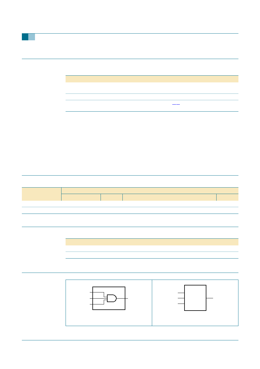
The 74LVC1G11 provides a single 3-input AND gate.
2.
Features
s
Wide supply voltage range from 1.65 V to 5.5 V
s
5 V tolerant inputs for interfacing with 5 V logic
s
High noise immunity
s
Complies with JEDEC standard:
x
JESD8-7 (1.65 V to 1.95 V)
x
JESD8-5 (2.3 V to 2.7 V)
x
JESD8-B/JESD36 (2.7 V to 3.6 V).
s
±
24 mA output drive (V
CC
= 3.0 V)
s
ESD protection:
x
HBM EIA/JESD22-A114-B exceeds 2000 V
x
MM EIA/JESD22-A115-A exceeds 200 V.
s
CMOS low power consumption
s
Latch-up performance exceeds 250 mA
s
Direct interface with TTL levels
s
Multiple package options
s
Specified from
-
40
°
C to +85
°
C and
-
40
°
C to +125
°
C.
74LVC1G11
Single 3-input AND gate
Rev. 01 -- 30 November 2004
Product data sheet
9397 750 14209
© Koninklijke Philips Electronics N.V. 2004. All rights reserved.
Product data sheet
Rev. 01 -- 30 November 2004
2 of 14
Philips Semiconductors
74LVC1G11
Single 3-input AND gate
3.
Quick reference data
[1]
C
PD
is used to determine the dynamic power dissipation (P
D
in
µ
W).
P
D
= C
PD
×
V
CC
2
×
f
i
×
N +
(C
L
×
V
CC
2
×
f
o
) where:
f
i
= input frequency in MHz;
f
o
= output frequency in MHz;
C
L
= output load capacitance in pF;
V
CC
= supply voltage in V;
N = number of inputs switching;
(C
L
×
V
CC
2
×
f
o
) = sum of the outputs.
[2]
The condition is V
I
= GND to V
CC
.
4.
Ordering information
5.
Marking
6.
Functional diagram
Table 1:
Quick reference data
GND = 0 V; T
amb
= 25
°
C; t
r
= t
f
2.5 ns.
Symbol
Parameter
Conditions
Min
Typ
Max
Unit
t
PHL
, t
PLH
propagation delay A,
B and C to Y
C
L
= 50 pF; V
CC
= 3.3 V
1.0
2.6
4.3
ns
C
I
input capacitance
-
4
-
pF
C
PD
power dissipation
capacitance
V
CC
= 3.3 V
[1] [2]
-
13
-
pF
Table 2:
Ordering information
Type number
Package
Temperature range
Name
Description
Version
74LVC1G11GW
-
40
°
C to +125
°
C
SC-88
plastic surface mounted package; 6 leads
SOT363
74LVC1G11GV
-
40
°
C to +125
°
C
SC-74
plastic surface mounted package; 6 leads
SOT457
Table 3:
Marking
Type number
Marking code
74LVC1G11GW
VU
74LVC1G11GV
V11
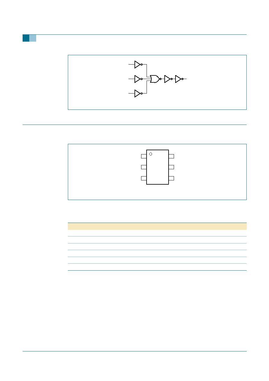
Fig 1.
Logic symbol
Fig 2.
IEC logic symbol
001aac033
A
B
C
1
3
4
Y
6
001aac029
&
4
1
3
6
9397 750 14209
© Koninklijke Philips Electronics N.V. 2004. All rights reserved.
Product data sheet
Rev. 01 -- 30 November 2004
3 of 14
Philips Semiconductors
74LVC1G11
Single 3-input AND gate
7.
Pinning information
7.1 Pinning
7.2 Pin description
Fig 3.
Logic diagram
001aac030
A
B
C
Y
Fig 4.
Pin configuration
11
A
C
GND
B
Y
001aac032
1
2
3
6
V
CC
5
4
Table 4:
Pin description
Symbol
Pin
Description
A
1
data input
GND
2
ground (0 V)
B
3
data input
Y
4
data output
V
CC
5
supply voltage
C
6
data input
9397 750 14209
© Koninklijke Philips Electronics N.V. 2004. All rights reserved.
Product data sheet
Rev. 01 -- 30 November 2004
4 of 14
Philips Semiconductors
74LVC1G11
Single 3-input AND gate
8.
Functional description
8.1 Function table
[1]
H = HIGH voltage level;
L = LOW voltage level;
X = don't care.
9.
Limiting values
[1]
The input and output voltage ratings may be exceeded if the input and output current ratings are observed.
[2]
When V
CC
= 0 V (Power-down mode), the output voltage can be 5.5 V in normal operation.
Table 5:
Function table
[1]
Input
Output
A
B
C
Y
H
H
H
H
L
X
X
L
X
L
X
L
X
X
L
L
Table 6:
Limiting values
In accordance with the Absolute Maximum Rating System (IEC 60134). Voltages are referenced to
GND (ground = 0 V).
Symbol
Parameter
Conditions
Min
Max
Unit
V
CC
supply voltage
-
0.5
+6.5
V
V
I
input voltage
[1]
-
0.5
+6.5
V
V
O
output voltage
active mode
[1] [2]
-
0.5
V
CC
+ 0.5 V
Power-down mode
[1] [2]
-
0.5
+6.5
V
I
IK
input diode current
V
I
< 0 V
-
-
50
mA
I
OK
output diode current
V
O
> V
CC
or V
O
< 0 V
-
±
50
mA
I
O
output source or sink
current
V
O
= 0 V to V
CC
-
±
50
mA
I
CC
, I
GND
V
CC
or GND current
-
±
100
mA
T
stg
storage temperature
-
65
+150
°
C
P
tot
power dissipation
T
amb
=
-
40
°
C to +125
°
C
-
250
mW
9397 750 14209
© Koninklijke Philips Electronics N.V. 2004. All rights reserved.
Product data sheet
Rev. 01 -- 30 November 2004
5 of 14
Philips Semiconductors
74LVC1G11
Single 3-input AND gate
10. Recommended operating conditions
11. Static characteristics
Table 7:
Recommended operating conditions
Symbol
Parameter
Conditions
Min
Typ
Max
Unit
V
CC
supply voltage
1.65
-
5.5
V
V
I
input voltage
0
-
5.5
V
V
O
output voltage
active mode
0
-
V
CC
V
Power-down mode;
V
CC
= 0 V
0
-
5.5
V
T
amb
ambient temperature
-
40
-
+125
°
C
t
r
, t
f
input rise and fall times
V
CC
= 1.65 V to 2.7 V
0
-
20
ns/V
V
CC
= 2.7 V to 5.5 V
0
-
10
ns/V
Table 8:
Static characteristics
At recommended operating conditions; voltages are referenced to GND (ground = 0 V).
Symbol Parameter
Conditions
Min
Typ
Max
Unit
T
amb
=
-
40
°
C to +85
°
C
[1]
V
IH
HIGH-level input voltage V
CC
= 1.65 V to 1.95 V
0.65
×
V
CC
-
-
V
V
CC
= 2.3 V to 2.7 V
1.7
-
-
V
V
CC
= 2.7 V to 3.6 V
2.0
-
-
V
V
CC
= 4.5 V to 5.5 V
0.7
×
V
CC
-
-
V
V
IL
LOW-level input voltage
V
CC
= 1.65 V to 1.95 V
-
-
0.35
×
V
CC
V
V
CC
= 2.3 V to 2.7 V
-
-
0.7
V
V
CC
= 2.7 V to 3.6 V
-
-
0.8
V
V
CC
= 4.5 V to 5.5 V
-
-
0.3
×
V
CC
V
V
OH
HIGH-level output
voltage
V
I
= V
IH
or V
IL
I
O
=
-
100
µ
A; V
CC
= 1.65 V to 5.5 V
V
CC
-
0.1
-
-
V
I
O
=
-
4 mA; V
CC
= 1.65 V
1.2
1.54
-
V
I
O
=
-
8 mA; V
CC
= 2.3 V
1.9
2.15
-
V
I
O
=
-
12 mA; V
CC
= 2.7 V
2.2
2.50
-
V
I
O
=
-
24 mA; V
CC
= 3.0 V
2.3
2.62
-
V
I
O
=
-
32 mA; V
CC
= 4.5 V
3.8
4.11
-
V
V
OL
LOW-level output
voltage
V
I
= V
IH
or V
IL
I
O
= 100
µ
A; V
CC
= 1.65 V to 5.5 V
-
-
0.10
V
I
O
= 4 mA; V
CC
= 1.65 V
-
0.07
0.45
V
I
O
= 8 mA; V
CC
= 2.3 V
-
0.12
0.30
V
I
O
= 12 mA; V
CC
= 2.7 V
-
0.17
0.40
V
I
O
= 24 mA; V
CC
= 3.0 V
-
0.33
0.55
V
I
O
= 32 mA; V
CC
= 4.5 V
-
0.39
0.55
V
I
LI
input leakage current
V
I
= 5.5 V or GND; V
CC
= 5.5 V
-
±
0.1
±
5
µ
A
I
off
power-off leakage
current
V
I
or V
O
= 5.5 V; V
CC
= 0 V
-
±
0.1
±
10
µ
A
Document Outline