2003 Jul 25
2
Philips Semiconductors
Product specification
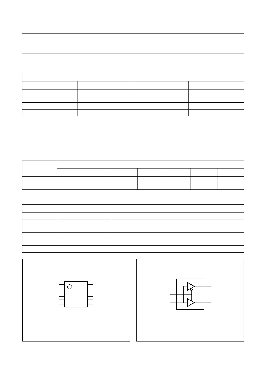
1-of-2 non-inverting demultiplexer with
3-state deselected output
74LVC1G18
FEATURES
·
Wide supply voltage range from 1.65 to 5.5 V
·
5 V tolerant input/output for interfacing with 5 V logic
·
High noise immunity
·
Complies with JEDEC standard:
JESD8-7 (1.65 to 1.95 V)
JESD8-5 (2.3 to 2.7 V)
JESD8B/JESD36 (2.7 to 3.6 V).
·
ESD protection:
HBM EIA/JESD22-A114-A exceeds 2000 V
MM EIA/JESD22-A115-A exceeds 200 V.
· ±
24 mA output drive (V
CC
= 3.0 V)
·
CMOS low power consumption
·
Latch-up performance exceeds 250 mA
·
Direct interface with TTL levels
·
SOT363 and SOT457 package
·
Specified from
-
40 to +85
°
C and
-
40 to +125
°
C.
DESCRIPTION
The 74LVC1G18 is a high-performance, low-power,
low-voltage, Si-gate CMOS device, superior to most
advanced CMOS compatible TTL families.
Input can be driven from either 3.3 or 5 V devices. These
features allow the use of these devices in a mixed
3.3 and 5 V environment.
This device is fully specified for partial power-down
applications using I
off
. The I
off
circuitry disables the output,
preventing the damaging backflow current through the
device when it is powered down.
The 74LVC1G18 is a 1-of-2 non-inverting demultiplexer
with a 3-state output. The 74LVC1G18 buffers the data on
input pin A and passes it either to output 1Y or 2Y,
depending on whether the state of the select input (pin S)
is LOW or HIGH.
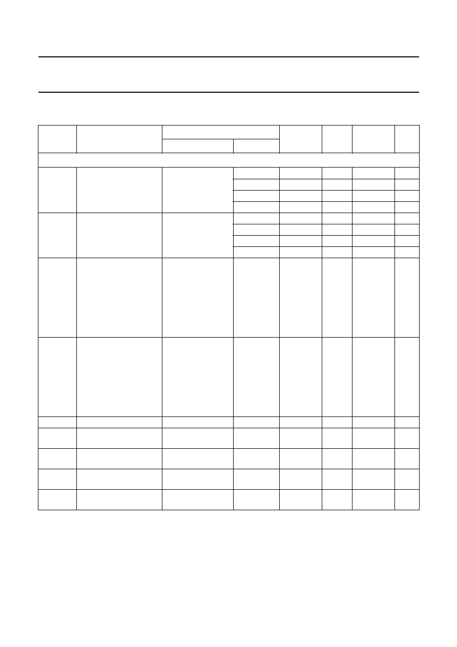
QUICK REFERENCE DATA
GND = 0 V; T
amb
= 25
°
C.
Notes
1. C
PD
is used to determine the dynamic power dissipation (P
D
in
µ
W).
P
D
= C
PD
×
V
CC
2
×
f
i
×
N +
(C
L
×
V
CC
2
×
f
o
) where:
f
i
= input frequency in MHz;
f
o
= output frequency in MHz;
C
L
= output load capacitance in pF;
V
CC
= supply voltage in Volts;
N = total load switching outputs;
(C
L
×
V
CC
2
×
f
o
) = sum of outputs.
2. The condition is V
I
= GND to V
CC
.
SYMBOL
PARAMETER
CONDITIONS
TYPICAL
UNIT
t
PHL
/t
PLH
propagation delay input A to output nY
V
CC
= 1.8 V; C
L
= 30 pF; R
L
= 1 k
5.1
ns
V
CC
= 2.5 V; C
L
= 30 pF; R
L
= 500
3.2
ns
V
CC
= 2.7 V; C
L
= 50 pF; R
L
= 500
3.2
ns
V
CC
= 3.3 V; C
L
= 50 pF; R
L
= 500
3.0
ns
V
CC
= 5.0 V; C
L
= 50 pF; R
L
= 500
2.3
ns
C
I
input capacitance
2.5
pF
C
PD
power dissipation capacitance per gate
V
CC
= 3.3 V; notes 1 and 2
28.8
pF
2003 Jul 25
4
Philips Semiconductors
Product specification
1-of-2 non-inverting demultiplexer with
3-state deselected output
74LVC1G18
RECOMMENDED OPERATING CONDITIONS
LIMITING VALUES
In accordance with the Absolute Maximum Rating System (IEC 60134); voltages are referenced to GND (ground = 0 V).
Notes
1. The input and output voltage ratings may be exceeded if the input and output current ratings are observed.
2. When V
CC
= 0 V (Power-down mode), the output voltage can be 5.5 V in normal operation.
SYMBOL
PARAMETER
CONDITIONS
MIN.
MAX.
UNIT
V
CC
supply voltage
1.65
5.5
V
V
I
input voltage
0
5.5
V
V
O
output voltage
active mode
0
V
CC
V
V
CC
= 0 V; Power-down or
high-impedance state
0
5.5
V
T
amb
operating ambient temperature
-
40
+125
°
C
t
r
, t
f
input rise and fall times
V
CC
= 1.65 to 2.7 V
0
20
ns/V
V
CC
= 2.7 to 5.5 V
0
10
ns/V
SYMBOL
PARAMETER
CONDITIONS
MIN.
MAX.
UNIT
V
CC
supply voltage
-
0.5
+6.5
V
I
IK
input diode current
V
I
< 0
-
-
50
mA
V
I
input voltage
note 1
-
0.5
+6.5
V
I
OK
output diode current
V
O
> V
CC
or V
O
< 0
-
±
50
mA
V
O
output voltage
active mode; notes 1 and 2
-
0.5
V
CC
+ 0.5
V
Power-down mode; notes 1 and 2
-
0.5
+6.5
V
I
O
output source or sink current
V
O
= 0 to V
CC
-
±
50
mA
I
CC
, I
GND
V
CC
or GND current
-
±
100
mA
T
stg
storage temperature
-
65
+150
°
C
P
D
power dissipation
T
amb
=
-
40 to +125
°
C
-
300
mW
2003 Jul 25
5
Philips Semiconductors
Product specification
1-of-2 non-inverting demultiplexer with
3-state deselected output
74LVC1G18
DC CHARACTERISTICS
At recommended operating conditions; voltages are referenced to GND (ground = 0 V).
SYMBOL
PARAMETER
TEST CONDITIONS
MIN.
TYP.
MAX.
UNIT
OTHER
V
CC
(V)
T
amb
=
-
40 to +85
°
C; note 1
V
IH
HIGH-level input voltage
1.65 to 1.95
0.65
×
V
CC
-
-
V
2.3 to 2.7
1.7
-
-
V
2.7 to 3.6
2.0
-
-
V
4.5 to 5.5
0.7
×
V
CC
-
-
V
V
IL
LOW-level input voltage
1.65 to 1.95
-
-
0.35
×
V
CC
V
2.3 to 2.7
-
-
0.7
V
2.7 to 3.6
-
-
0.8
V
4.5 to 5.5
-
-
0.3
×
V
CC
V
V
OL
LOW-level output voltage V
I
= V
IH
or V
IL
I
O
= 100
µ
A
1.65 to 5.5
-
-
0.1
V
I
O
= 4 mA
1.65
-
-
0.45
V
I
O
= 8 mA
2.3
-
-
0.3
V
I
O
= 12 mA
2.7
-
-
0.4
V
I
O
= 24 mA
3.0
-
-
0.55
V
I
O
= 32 mA
4.5
-
-
0.55
V
V
OH
HIGH-level output
voltage
V
I
= V
IH
or V
IL
I
O
=
-
100
µ
A
1.65 to 5.5
V
CC
-
0.1
-
-
V
I
O
=
-
4 mA
1.65
1.2
-
-
V
I
O
=
-
8 mA
2.3
1.9
-
-
V
I
O
=
-
12 mA
2.7
2.2
-
-
V
I
O
=
-
24 mA
3.0
2.3
-
-
V
I
O
=
-
32 mA
4.5
3.8
-
-
V
I
LI
input leakage current
V
I
= 5.5 V or GND
5.5
-
±
0.1
±
5
µ
A
I
OZ
3-state output OFF-state
current
V
I
= V
IH
or V
IL
;
V
O
= V
CC
or GND
5.5
-
±
0.1
±
10
µ
A
I
off
power OFF leakage
current
V
I
or V
O
= 5.5 V
0
-
±
0.1
±
10
µ
A
I
CC
quiescent supply current
V
I
= V
CC
or GND;
I
O
= 0
5.5
-
0.1
10
µ
A
I
CC
additional quiescent
supply current per pin
V
I
= V
CC
-
0.6 V;
I
O
= 0
2.3 to 5.5
-
5
500
µ
A