 | ÐлекÑÑоннÑй компоненÑ: 74LVC1G53 | СкаÑаÑÑ:  PDF PDF  ZIP ZIP |
74LVC1G53 2-channel analog multiplexer/demultiplexer
1.
General description
The 74LVC1G53 is a high-performance, low-power, low-voltage, Si-gate CMOS device
that provides superior performance to most advanced CMOS compatible TTL families.
The 74LVC1G53 provides one analog multiplexer/demultiplexer with a digital select
input (S), two independent inputs/outputs (B0 and B1), a common input/output (A) and an
active LOW enable input (E). When pin E is HIGH, the switch is turned off.
The 74LVC1G53 can handle both analog and digital signals.
2.
Features
s
Wide supply voltage range from 1.65 V to 5.5 V
s
Very low ON resistance:
x
7.5
(typical) at V
CC
= 2.7 V
x
6.5
(typical) at V
CC
= 3.3 V
x
6
(typical) at V
CC
= 5 V
s
High noise immunity
s
ESD protection:
x
HBM JESD22-A114-C exceeds 2000 V
x
MM JESD22-A115-A exceeds 200 V
x
CDM JESD22-C101-C exceeds 1000 V
s
CMOS low-power consumption
s
Latch-up performance meets requirements of JESD 78 Class I
s
Direct interface with TTL levels
s
Control inputs accepts voltages up to 5 V
s
Multiple package options
s
Specified from
-
40
°
C to +85
°
C and from
-
40
°
C to +125
°
C
74LVC1G53
2-channel analog multiplexer/demultiplexer
Rev. 01 -- 10 January 2006
Product data sheet
74LVC1G53_1
© Koninklijke Philips Electronics N.V. 2006. All rights reserved.
Product data sheet
Rev. 01 -- 10 January 2006
2 of 23
Philips Semiconductors
74LVC1G53
2-channel analog multiplexer/demultiplexer
3.
Quick reference data
4.
Ordering information
5.
Marking
Table 1:
Quick reference data
GND = 0 V; t
r
= t
f
2.5 ns; minimum and maximum values at T
amb
=
-
40
°
C to +85
°
C;
typical values at T
amb
= 25
°
C.
Symbol
Parameter
Conditions
Min
Typ
Max
Unit
t
on
turn-on time
S to A or Bn
C
L
= 50 pF; R
L
= 500
V
CC
= 3.3 V
1.8
3.4
5.0
ns
V
CC
= 5.0 V
1.3
2.6
3.8
ns
E to A or Bn
C
L
= 50 pF; R
L
= 500
V
CC
= 3.3 V
1.2
2.2
3.8
ns
V
CC
= 5.0 V
1.0
1.7
2.6
ns
t
off
turn-off time
S to A or Bn
C
L
= 50 pF; R
L
= 500
V
CC
= 3.3 V
1.1
4.0
5.4
ns
V
CC
= 5.0 V
1.0
2.9
3.8
ns
E to A or Bn
C
L
= 50 pF; R
L
= 500
V
CC
= 3.3 V
2.0
3.7
5.0
ns
V
CC
= 5.0 V
1.3
2.9
3.8
ns
C
i
input capacitance
-
2.5
-
pF
C
S(OFF)
OFF-state capacitance
-
6.0
-
pF
C
S(ON)
ON-state capacitance
-
18
-
pF
Table 2:
Ordering information
Type number
Package
Temperature range Name
Description
Version
74LVC1G53DC
-
40
°
C to +125
°
C
VSSOP8
plastic very thin shrink small
outline package; 8 leads;
body width 2.3 mm
SOT765-1
74LVC1G53GT
-
40
°
C to +125
°
C
XSON8
plastic extremely thin small outline
package; no leads; 8 terminals;
body 1
×
1.95
×
0.5 mm
SOT833-1
Table 3:
Marking
Type number
Marking code
74LVC1G53DC
V53
74LVC1G53GT
V53
74LVC1G53_1
© Koninklijke Philips Electronics N.V. 2006. All rights reserved.
Product data sheet
Rev. 01 -- 10 January 2006
3 of 23
Philips Semiconductors
74LVC1G53
2-channel analog multiplexer/demultiplexer
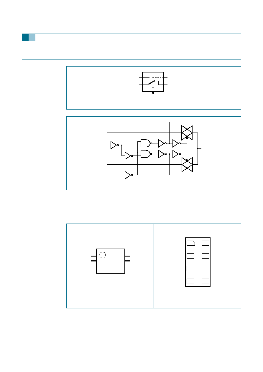
6.
Functional diagram
7.
Pinning information
7.1 Pinning
Fig 1.
Logic symbol
Fig 2.
Logic diagram
001aad386
S
A
E
B0
B1
6
7
2
5
1
001aad387
A
B0
S
B1
E
Fig 3.
Pin configuration VSSOP8
Fig 4.
Pin configuration XSON8
53
A
V
CC
E
B0
GND
B1
GND
S
001aad388
1
2
3
4
6
5
8
7
53
B1
B0
V
CC
S
GND
E
A
GND
001aad389
3
6
2
7
1
8
4
5
Transparent top view
74LVC1G53_1
© Koninklijke Philips Electronics N.V. 2006. All rights reserved.
Product data sheet
Rev. 01 -- 10 January 2006
4 of 23
Philips Semiconductors
74LVC1G53
2-channel analog multiplexer/demultiplexer
7.2 Pin description
8.
Functional description
8.1 Function table
[1]
H = HIGH voltage level;
L = LOW voltage level;
X = don't care;
Z = high-impedance OFF-state.
Table 4:
Pin description
Symbol
Pin
Description
A
1
common A output or input
E
2
enable input (active LOW)
GND
3
ground (0 V)
GND
4
ground (0 V)
S
5
select input
B1
6
independent B1 input or output
B0
7
independent B0 input or output
V
CC
8
supply voltage
Table 5:
Function table
[1]
Input
Channel on
S
E
L
L
B0 to A or A to B0
H
L
B1 to A or A to B1
X
H
Z (switch off)
74LVC1G53_1
© Koninklijke Philips Electronics N.V. 2006. All rights reserved.
Product data sheet
Rev. 01 -- 10 January 2006
5 of 23
Philips Semiconductors
74LVC1G53
2-channel analog multiplexer/demultiplexer
9.
Limiting values
[1]
The input and output voltage ratings may be exceeded if the input and output current ratings are observed.
[2]
For VSSOP8 package: above 110
°
C the value of P
tot
derates linearly with 8 mW/K.
For XSON8 package: above 45
°
C the value of P
tot
derates linearly with 2.4 mW/K.
10. Recommended operating conditions
[1]
To avoid drawing V
CC
current out of terminal A when switch current flows in terminal Bn, the voltage drop
across the bidirectional switch must not exceed 0.4 V. If the switch current flows into terminal A, no V
CC
current will flow out of terminal Bn. In this case, there is no limit for the voltage drop across the switch.
[2]
Applies to control signal levels.
Table 6:
Limiting values
In accordance with the Absolute Maximum Rating System (IEC 60134).
Voltages are referenced to GND (ground = 0 V).
Symbol
Parameter
Conditions
Min
Max
Unit
V
CC
supply voltage
-
0.5
+6.5
V
V
I
input voltage
[1]
-
0.5
+6.5
V
I
IK
input clamping
current
V
I
<
-
0.5 V or V
I
> V
CC
+ 0.5
-
-
50
mA
I
SK
switch clamping
current
V
I
<
-
0.5 V or V
I
> V
CC
+ 0.5
-
±
50
mA
V
SW
switch voltage
enable and disable mode
-
0.5
V
CC
+ 0.5 V
I
SW
switch current
V
SW
=
-
0.5 V to (V
CC
+ 0.5 V)
-
±
50
mA
I
CC
quiescent supply
current
-
100
mA
I
GND
ground current
-
-
100
mA
T
stg
storage temperature
-
65
+
150
°
C
P
tot
total power
dissipation
T
amb
=
-
40
°
C to +125
°
C
[2]
-
300
mW
Table 7:
Recommended operating conditions
Symbol
Parameter
Conditions
Min
Typ
Max
Unit
V
CC
supply voltage
1.65
-
5.5
V
V
I
input voltage
0
-
5.5
V
V
SW
switch voltage
enable and disable
mode
[1]
0
-
V
CC
V
T
amb
ambient temperature
-
40
-
+125
°
C
t/
V
input transition rise and
fall rate
V
CC
= 1.65 V to 2.7 V
[2]
0
-
20
ns/V
V
CC
= 2.7 V to 5.5 V
[2]
0
-
10
ns/V
Document Outline