2005 Feb 01
2
Philips Semiconductors
Product specification
Single D-type flip-flop with set and
reset; positive edge trigger
74LVC1G74
FEATURES
∑
Wide supply voltage range from 1.65 V to 5.5 V
∑
5 V tolerant inputs for interfacing with 5 V logic
∑
High noise immunity
∑
Complies with JEDEC standard:
≠ JESD8-7 (1.65 V to 1.95 V)
≠ JESD8-5 (2.3 V to 2.7 V)
≠ JESD8B/JESD36 (2.7 V to 3.6 V).
∑ ±
24 mA output drive (V
CC
= 3.0 V)
∑
ESD protection:
≠ HBM EIA/JESD22-A114-B exceeds 2000 V
≠ MM EIA/JESD22-A115-A exceeds 200 V.
∑
CMOS low power consumption
∑
Latch-up performance exceeds 250 mA
∑
Direct interface with TTL levels
∑
Inputs accept voltages up to 5 V
∑
Multiple package options
∑
Specified from
-
40
∞
C to +85
∞
C and
-
40
∞
C to +125
∞
C.
DESCRIPTION
The 74LVC1G74 is a high-performance, low-voltage,
Si-gate CMOS device, superior to most advanced CMOS
compatible TTL families.
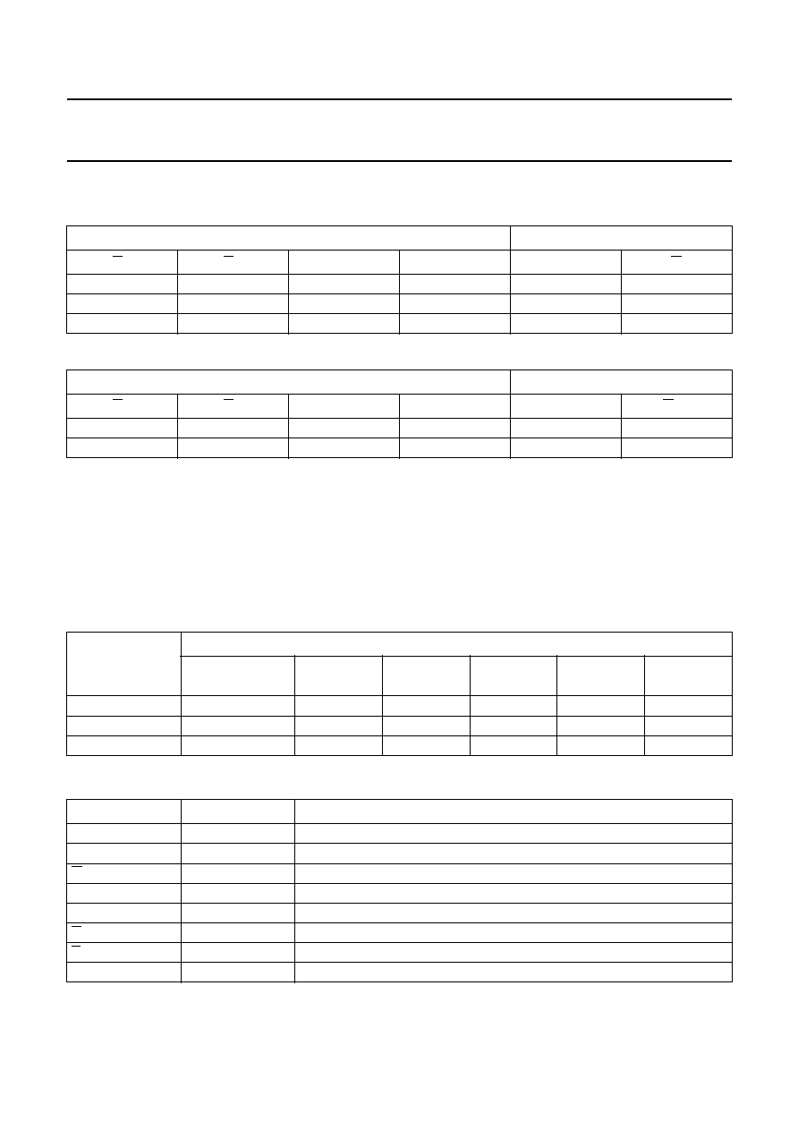
The 74LVC1G74 is a single positive edge triggered D-type
flip-flop with individual data (D) inputs, clock (CP) inputs,
set (SD) and (RD) inputs, and complementary Q and Q
outputs.
This device is fully specified for partial power down
applications using I
off
. The I
off
circuitry disables the output,
preventing damaging backflow current through the device
when it is powered down.
The set and reset are asynchronous active LOW inputs
and operate independently of the clock input. Information
on the data input is transferred to the Q output on the
LOW-to-HIGH transition of the clock pulse. The D inputs
must be stable one set-up time prior to the LOW-to-HIGH
clock transition, for predictable operation.
Schmitt-trigger action at all inputs makes the circuit highly
tolerant to slower input rise and fall times.
QUICK REFERENCE DATA
GND = 0 V; T
amb
= 25
∞
C; t
r
= t
f
2.5 ns.
Notes
1. C
PD
is used to determine the dynamic power dissipation (P
D
in
µ
W).
P
D
= C
PD
◊
V
CC
2
◊
f
i
◊
N +
(C
L
◊
V
CC
2
◊
f
o
) where:
f
i
= input frequency in MHz;
f
o
= output frequency in MHz;
C
L
= output load capacitance in pF;
V
CC
= supply voltage in Volts;
N = number of inputs switching;
(C
L
◊
V
CC
2
◊
f
o
) = sum of the outputs.
2. The condition is V
I
= GND to V
CC
.
SYMBOL
PARAMETER
CONDITIONS
TYPICAL
UNIT
t
PHL
/t
PLH
propagation delay
CP to Q, Q
C
L
= 50 pF; V
CC
= 3.3 V
3.5
ns
SD to Q, Q
C
L
= 50 pF; V
CC
= 3.3 V
3.0
ns
RD to Q, Q
C
L
= 50 pF; V
CC
= 3.3 V
3.0
ns
f
max
maximum clock frequency
C
L
= 50 pF; V
CC
= 3.3 V
280
MHz
C
I
input capacitance
4.0
pF
C
PD
power dissipation capacitance
V
CC
= 3.3 V; notes 1 and 2
15
pF
2005 Feb 01
3
Philips Semiconductors
Product specification
Single D-type flip-flop with set and
reset; positive edge trigger
74LVC1G74
FUNCTION TABLES
Table 1
Asynchronous operation. See note 1.
Table 2
Synchronous operation. See note 1.
Note to Tables 1 and 2
1. H = HIGH voltage level;
L = LOW voltage level;
X = don't care;
= LOW-to-HIGH CP transition;
Q
n+1
= state after the next LOW-to-HIGH CP transition.
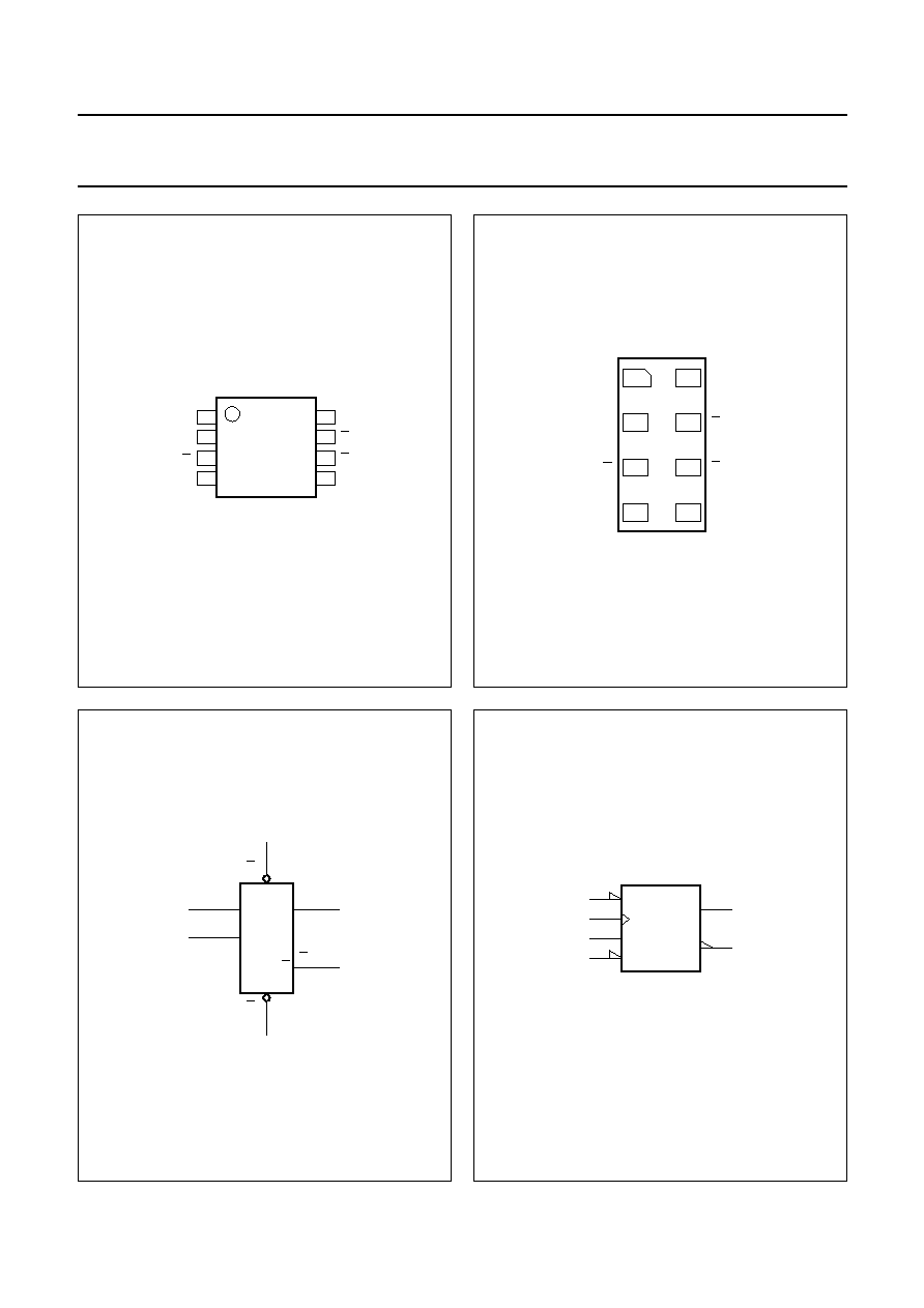
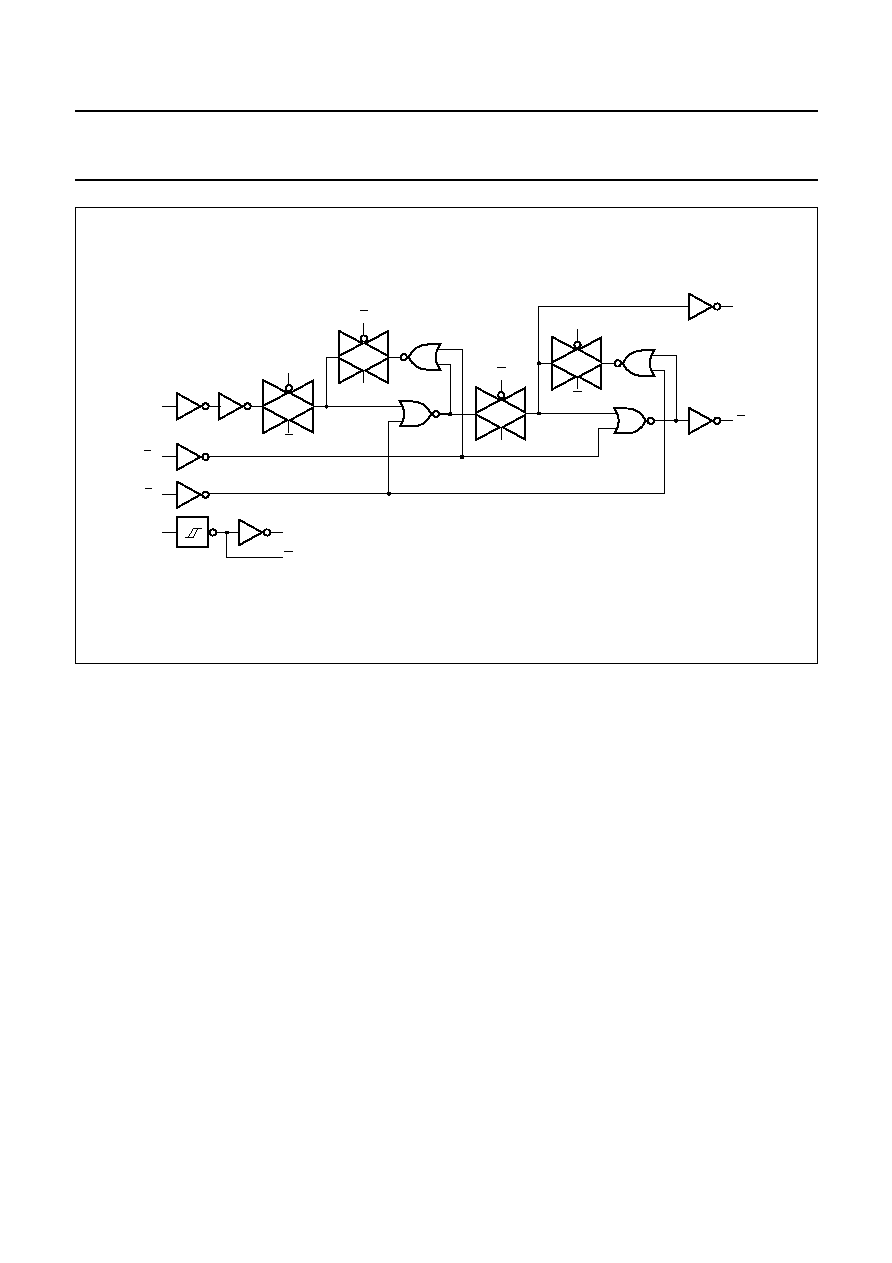
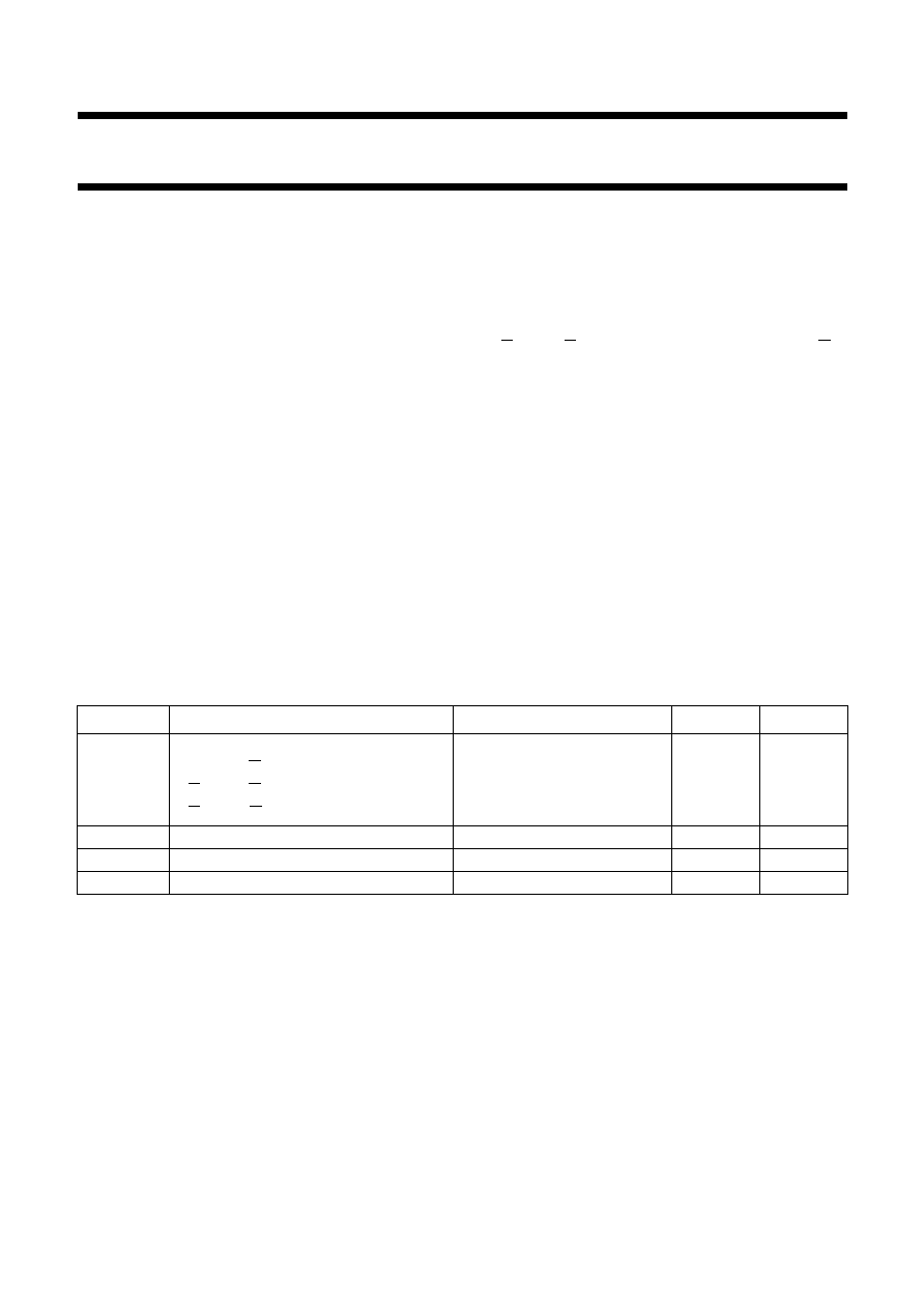
ORDERING INFORMATION
PINNING
INPUT
OUTPUT
SD
RD
CP
D
Q
Q
L
H
X
X
H
L
H
L
X
X
L
H
L
L
X
X
H
H
INPUT
OUTPUT
SD
RD
CP
D
Q
n+1
Q
n+1
H
H
L
L
H
H
H
H
H
L
TYPE NUMBER
PACKAGE
TEMPERATURE
RANGE
PINS
PACKAGE
MATERIAL
CODE
MARKING
74LVC1G74DP
-
40
∞
C to +125
∞
C
8
TSSOP8
plastic
SOT505-2
V74
74LVC1G74DC
-
40
∞
C to +125
∞
C
8
VSSOP8
plastic
SOT765-1
V74
74LVC1G74GT
-
40
∞
C to +125
∞
C
8
XSON8
plastic
SOT833-1
V74
SYMBOL
PIN
DESCRIPTION
CP
1
clock input (LOW-to-HIGH, edge-triggered)
D
2
data input
Q
3
complement flip-flop output
GND
4
ground (0 V)
Q
5
true flip-flop output
RD
6
asynchronous reset-direct input (active LOW)
SD
7
asynchronous set-direct input (active LOW)
V
CC
8
supply voltage