Äîêóìåíòàöèÿ è îïèñàíèÿ www.docs.chipfind.ru
DATA SHEET
Product specification
Supersedes data of 2004 Jun 28
2004 Sep 21
INTEGRATED CIRCUITS
74LVC1GU04
Inverter
2004 Sep 21
2
Philips Semiconductors
Product specification
Inverter
74LVC1GU04
FEATURES
·
Wide supply voltage range from 1.65 V to 5.5 V
·
High noise immunity
· ±
24 mA output drive (V
CC
= 3.0 V)
·
CMOS low power consumption
·
Latch-up performance exceeds 250 mA
·
Input accepts voltages up to 5 V
·
Multiple package options
·
ESD protection:
HBM EIA/JESD22-A114-B exceeds 2000 V
MM EIA/JESD22-A115-A exceeds 200 V.
·
Specified from
-
40
°
C to +85
°
C and
-
40
°
C to +125
°
C.
DESCRIPTION
The 74LVC1GU04 is a high-performance, low-power,
low-voltage, Si-gate CMOS device, superior to most
advanced CMOS compatible TTL families.
The input can be driven from either 3.3 V or 5 V devices.
This feature allows the use of this device in a mixed
3.3 V and 5 V environment.
Schmitt-trigger action at all inputs makes the circuit
tolerant for slower input rise and fall time.
The 74LVC1GU04 provides the inverting single state
unbuffered function.
QUICK REFERENCE DATA
Ground = 0 V; T
amb
= 25
°
C; t
r
= t
f
2.5 ns.
Notes
1. C
PD
is used to determine the dynamic power dissipation (P
D
in
µ
W).
P
D
= C
PD
×
V
CC
2
×
f
i
×
N +
(C
L
×
V
CC
2
×
f
o
) where:
f
i
= input frequency in MHz;
f
o
= output frequency in MHz;
C
L
= output load capacitance in pF;
V
CC
= supply voltage in Volts;
N = total load switching outputs;
(C
L
×
V
CC
2
×
f
o
) = sum of the outputs.
2. The condition is V
I
= GND to V
CC
.
SYMBOL
PARAMETER
CONDITIONS
TYPICAL
UNIT
t
PHL
/t
PLH
propagation delay A to Y
V
CC
= 1.8 V; C
L
= 30 pF; R
L
= 1 k
1.7
ns
V
CC
= 2.5 V; C
L
= 30 pF; R
L
= 500
1.3
ns
V
CC
= 2.7 V; C
L
= 50 pF; R
L
= 500
1.7
ns
V
CC
= 3.3 V; C
L
= 50 pF; R
L
= 500
1.6
ns
V
CC
= 5.0 V; C
L
= 50 pF; R
L
= 500
1.3
ns
C
I
input capacitance
6
pF
C
PD
power dissipation capacitance
V
CC
= 3.3 V; notes 1 and 2
14.9
pF
2004 Sep 21
3
Philips Semiconductors
Product specification
Inverter
74LVC1GU04
FUNCTION TABLE
See note 1.
Note
1. H = HIGH voltage level;
L = LOW voltage level.
ORDERING INFORMATION
PINNING
INPUT
OUTPUT
A
Y
L
H
H
L
TYPE NUMBER
PACKAGE
TEMPERATURE
RANGE
PINS
PACKAGE
MATERIAL
CODE
MARKING
74LVC1GU04GW
-
40
°
C to +125
°
C
5
SC-88A
plastic
SOT353
VD
74LVC1GU04GV
-
40
°
C to +125
°
C
5
SC-74A
plastic
SOT753
VU4
74LVC1GU04GM
-
40
°
C to +125
°
C
6
XSON6
plastic
SOT886
VD
PIN SC-88A; SC-74A
PIN XSON6
SYMBOL
DESCRIPTION
1
1
n.c.
not connected
2
2
A
data input A
3
3
GND
ground (0 V)
4
4
Y
data output Y
-
5
n.c.
not connected
5
6
V
CC
supply voltage
U04
n.c.
V
CC
A
GND
Y
001aab666
1
2
3
5
4
Fig.1 Pin configuration SC-88A and SC-77A.
U04
A
001aab667
n.c.
GND
n.c.
V
CC
Y
Transparent top view
2
3
1
5
4
6
Fig.2 Pin configuration XSON6.
2004 Sep 21
4
Philips Semiconductors
Product specification
Inverter
74LVC1GU04
handbook, halfpage
MNA108
A
Y
2
4
Fig.3 Logic symbol.
handbook, halfpage
MNA109
4
1
2
Fig.4 IEEE logic symbol.
handbook, halfpage
MNA636
A
Y
100
VCC VCC
Fig.5 Logic diagram.

2004 Sep 21
5
Philips Semiconductors
Product specification
Inverter
74LVC1GU04
RECOMMENDED OPERATING CONDITIONS
LIMITING VALUES
In accordance with the Absolute Maximum Rating System (IEC 60134); voltages are referenced to GND (ground = 0 V).
Notes
1. The input and output voltage ratings may be exceeded if the input and output current ratings are observed.
2. Above 55
°
C the value of P
tot
derates linearly with 4.5 mW/K.
SYMBOL
PARAMETER
CONDITIONS
MIN.
MAX.
UNIT
V
CC
supply voltage
1.65
5.5
V
V
I
input voltage
0
5.5
V
V
O
output voltage
0
V
CC
V
T
amb
operating ambient temperature
-
40
+125
°
C
t
r
, t
f
input rise and fall times
V
CC
= 1.65 V to 2.7 V
0
20
ns/V
V
CC
= 2.7 V to 5.5 V
0
10
ns/V
SYMBOL
PARAMETER
CONDITIONS
MIN.
MAX.
UNIT
V
CC
supply voltage
-
0.5
+6.5
V
I
IK
input diode current
V
I
< 0 V
-
-
50
mA
V
I
input voltage
note 1
-
0.5
+6.5
V
I
OK
output diode current
V
O
> V
CC
or V
O
< 0 V
-
±
50
mA
V
O
output voltage
active mode; note 1
-
0.5
V
CC
+ 0.5
V
I
O
output source or sink current
V
O
= 0 V to V
CC
-
±
50
mA
I
CC
, I
GND
V
CC
or GND current
-
±
100
mA
T
stg
storage temperature
-
65
+150
°
C
P
tot
power dissipation
T
amb
=
-
40
°
C to +125
°
C; note 2
-
200
mW
2004 Sep 21
6
Philips Semiconductors
Product specification
Inverter
74LVC1GU04
DC CHARACTERISTICS
At recommended operating conditions; voltages are referenced to GND (ground = 0 V).
SYMBOL
PARAMETER
TEST CONDITIONS
MIN.
TYP.
(1)
MAX.
UNIT
OTHER
V
CC
(V)
T
amb
=
-
40
°
C to +85
°
C
V
IH
HIGH-level input voltage
1.65 to 5.5
0.75
×
V
CC
-
-
V
V
IL
LOW-level input voltage
1.65 to 5.5
-
-
0.25
×
V
CC
V
V
OL
LOW-level output voltage V
I
= V
IH
or V
IL
I
O
= 100
µ
A
1.65 to 5.5
-
-
0.1
V
I
O
= 4 mA
1.65
-
-
0.45
V
I
O
= 8 mA
2.3
-
-
0.3
V
I
O
= 12 mA
2.7
-
-
0.4
V
I
O
= 24 mA
3.0
-
-
0.55
V
I
O
= 32 mA
4.5
-
-
0.55
V
V
OH
HIGH-level output
voltage
V
I
= V
IH
or V
IL
I
O
=
-
100
µ
A
1.65 to 5.5
V
CC
-
0.1
-
-
V
I
O
=
-
4 mA
1.65
1.2
-
-
V
I
O
=
-
8 mA
2.3
1.9
-
-
V
I
O
=
-
12 mA
2.7
2.2
-
-
V
I
O
=
-
24 mA
3.0
2.3
-
-
V
I
O
=
-
32 mA
4.5
3.8
-
-
V
I
LI
input leakage current
V
I
= 5.5 V or GND
3.6
-
±
0.1
±
5
µ
A
I
CC
quiescent supply current
V
I
= V
CC
or GND;
I
O
= 0 A
5.5
-
0.1
10
µ
A
2004 Sep 21
7
Philips Semiconductors
Product specification
Inverter
74LVC1GU04
Note
1. All typical values are measured at V
CC
= 3.3 V and T
amb
= 25
°
C.
T
amb
=
-
40
°
C to +125
°
C
V
IH
HIGH-level input voltage
1.65 to 5.5
0.8
×
V
CC
-
-
V
V
IL
LOW-level input voltage
1.65 to 5.5
-
-
0.2
×
V
CC
V
V
OL
LOW-level output voltage V
I
= V
IH
or V
IL
I
O
= 100
µ
A
1.65 to 5.5
-
-
0.1
V
I
O
= 4 mA
1.65
-
-
0.70
V
I
O
= 8 mA
2.3
-
-
0.45
V
I
O
= 12 mA
2.7
-
-
0.60
V
I
O
= 24 mA
3.0
-
-
0.80
V
I
O
= 32 mA
4.5
-
-
0.80
V
V
OH
HIGH-level output
voltage
V
I
= V
IH
or V
IL
I
O
=
-
100
µ
A
1.65 to 5.5
V
CC
-
0.1
-
-
V
I
O
=
-
4 mA
1.65
0.95
-
-
V
I
O
=
-
8 mA
2.3
1.7
-
-
V
I
O
=
-
12 mA
2.7
1.9
-
-
V
I
O
=
-
24 mA
3.0
2.0
-
-
V
I
O
=
-
32 mA
4.5
3.4
-
-
V
I
LI
input leakage current
V
I
= 5.5 V or GND
3.6
-
±
0.1
±
5
µ
A
I
CC
quiescent supply current
V
I
= V
CC
or GND;
I
O
= 0 A
5.5
-
-
200
µ
A
SYMBOL
PARAMETER
TEST CONDITIONS
MIN.
TYP.
(1)
MAX.
UNIT
OTHER
V
CC
(V)
2004 Sep 21
8
Philips Semiconductors
Product specification
Inverter
74LVC1GU04
AC CHARACTERISTICS
GND = 0 V; t
r
= t
f
2.0 ns.
Note
1. All typical values are measured at T
amb
= 25
°
C.
AC WAVEFORMS
SYMBOL
PARAMETER
TEST CONDITIONS
MIN.
TYP.
(1)
MAX.
UNIT
WAVEFORMS
V
CC
(V)
T
amb
=
-
40
°
C to +85
°
C
t
PHL
/t
PLH
propagation delay A to Y
see Figs 6 and 9
1.65 to 1.95
0.3
1.7
5.0
ns
2.3 to 2.7
0.3
1.3
4.0
ns
2.7
0.5
1.7
5.0
ns
3.0 to 3.6
0.5
1.6
3.7
ns
4.5 to 5.5
0.5
1.3
3.0
ns
T
amb
=
-
40
°
C to +125
°
C
t
PHL
/t
PLH
propagation delay A to Y
see Figs 6 and 9
1.65 to 1.95
0.3
-
6.5
ns
2.3 to 2.7
0.3
-
5.5
ns
2.7
0.5
-
6.5
ns
3.0 to 3.6
0.5
-
5.0
ns
4.5 to 5.5
0.5
-
4.0
ns
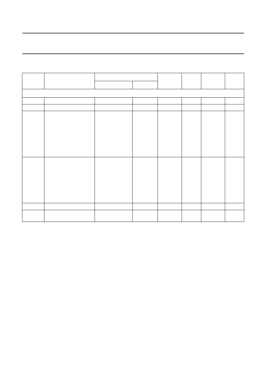
handbook, halfpage
MNA637
tPHL
tPLH
VM
VM
A input
Y output
GND
VI
VOH
VOL
Fig.6 Input A to output Y propagation delay times.
V
CC
V
M
INPUT
V
I
t
r
= t
f
1.65 V to 1.95 V
0.5
×
V
CC
V
CC
2.0 ns
2.3 V to 2.7 V
0.5
×
V
CC
V
CC
2.0 ns
2.7 V
1.5 V
2.7 V
2.5 ns
3.0 V to 3.6 V
1.5 V
2.7 V
2.5 ns
4.5 V to 5.5 V
0.5
×
V
CC
V
CC
2.5 ns
V
OL
and V
OH
are typical output voltage drop that occur with the output load.
2004 Sep 21
9
Philips Semiconductors
Product specification
Inverter
74LVC1GU04
handbook, halfpage
MNA638
VCC
Rbias = 560 k
input
0.47
µ
F
100
µ
F
output
A Io
Vi
Fig.7
Test set-up for measuring forward
transconductance.
f
i
= 1 kHz.
V
O
is constant.
G
fs
I
o
V
i
---------
=
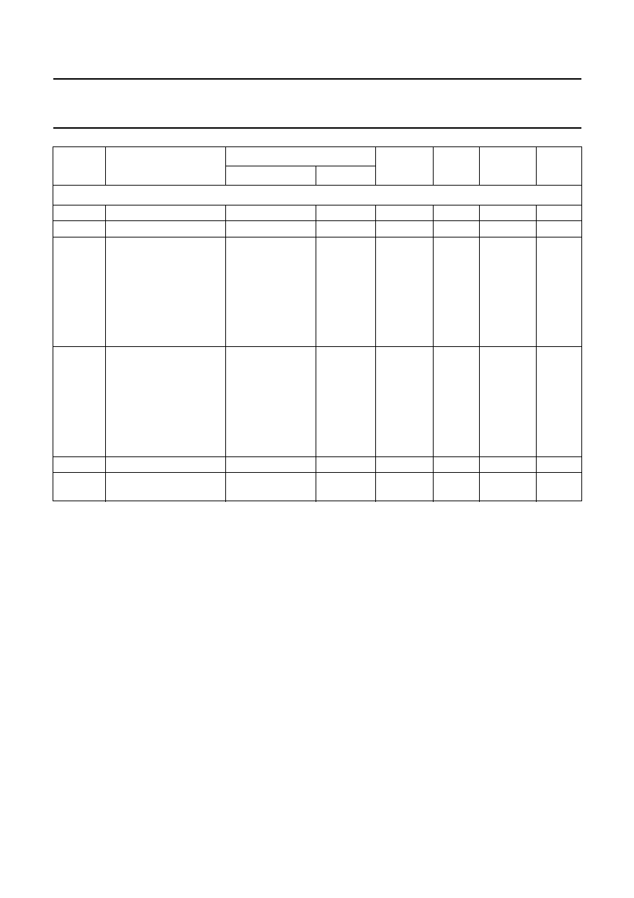
handbook, halfpage
0
2
4
6
120
100
40
0
80
20
60
MNA639
VCC (V)
Gfs
(mA/V)
Fig.8
Typical forward transconductance as a
function of supply voltage.
T
amb
= 25
°
C.
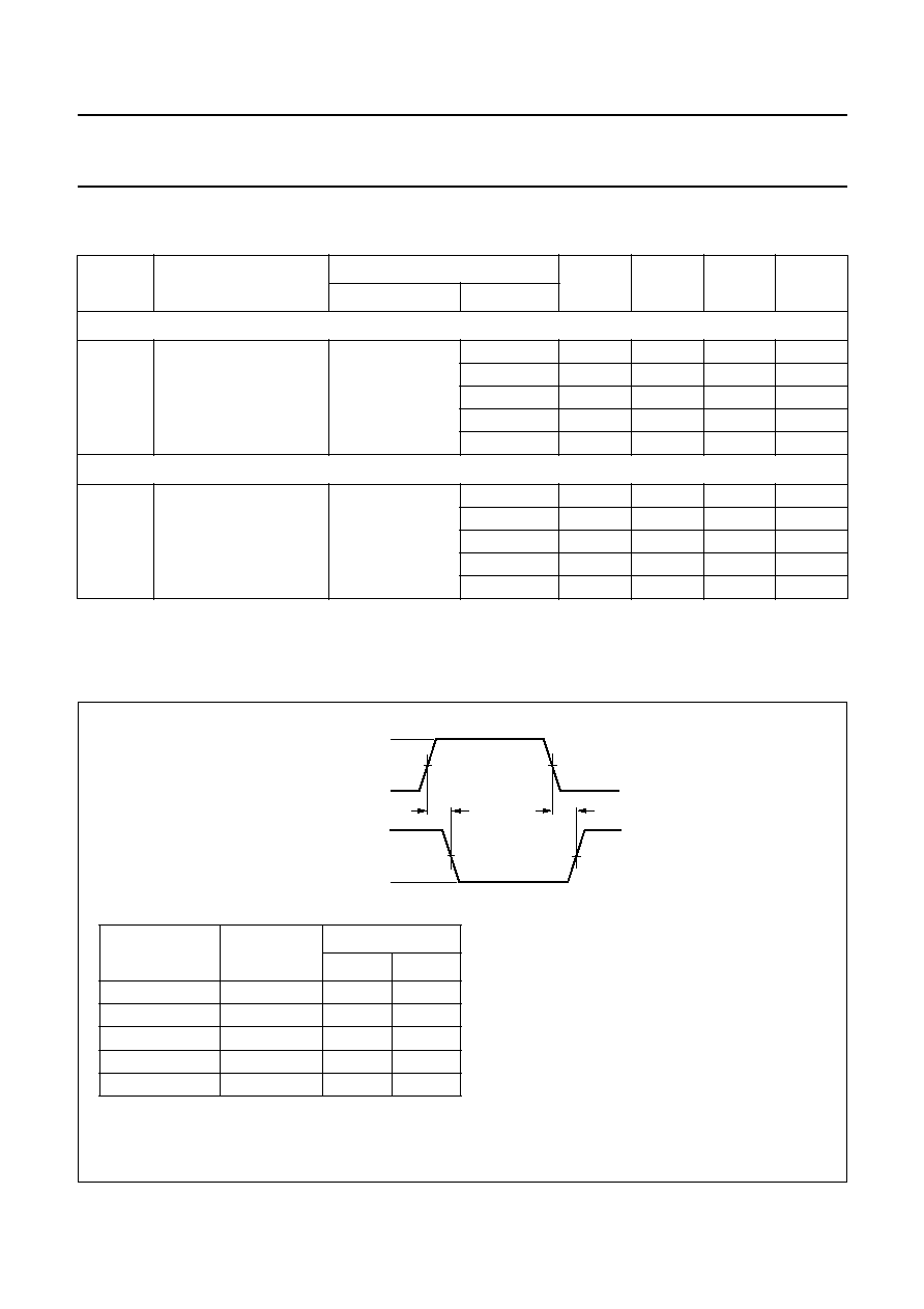
handbook, full pagewidth
VEXT
VCC
VI
VO
MNA616
D.U.T.
CL
RT
RL
RL
PULSE
GENERATOR
Fig.9 Load circuitry for switching times.
V
CC
V
I
C
L
R
L
V
EXT
t
PLH
/t
PHL
t
PZH
/t
PHZ
t
PZL
/t
PLZ
1.65 V to 1.95 V
V
CC
30 pF
1 k
open
GND
2
×
V
CC
2.3 V to 2.7 V
V
CC
30 pF
500
open
GND
2
×
V
CC
2.7 V
2.7 V
50 pF
500
open
GND
6 V
3.0 V to 3.6 V
2.7 V
50 pF
500
open
GND
6 V
4.5 V to 5.5 V
V
CC
50 pF
500
open
GND
2
×
V
CC
Definitions for test circuit:
R
L
= Load resistor.
C
L
= Load capacitance including jig and probe capacitance.
R
T
= Termination resistance should be equal to the output impedance Z
o
of the pulse generator.
2004 Sep 21
10
Philips Semiconductors
Product specification
Inverter
74LVC1GU04
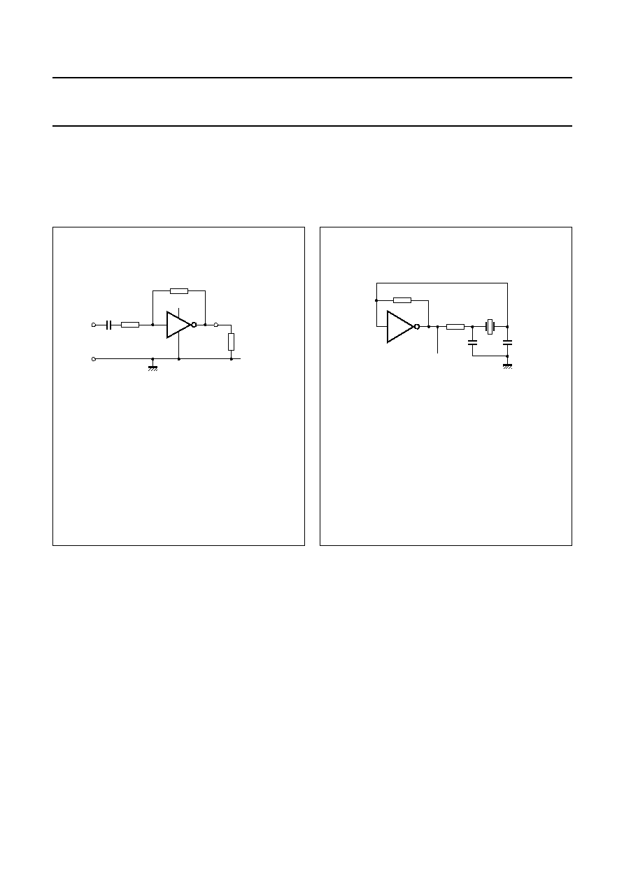
APPLICATION INFORMATION
Some applications for the 74LVC1GU04 are:
·
Linear amplifier (see Fig.10)
·
Crystal oscillator (see Fig.11).
Remark to the application information
All values given are typical values unless otherwise
specified.
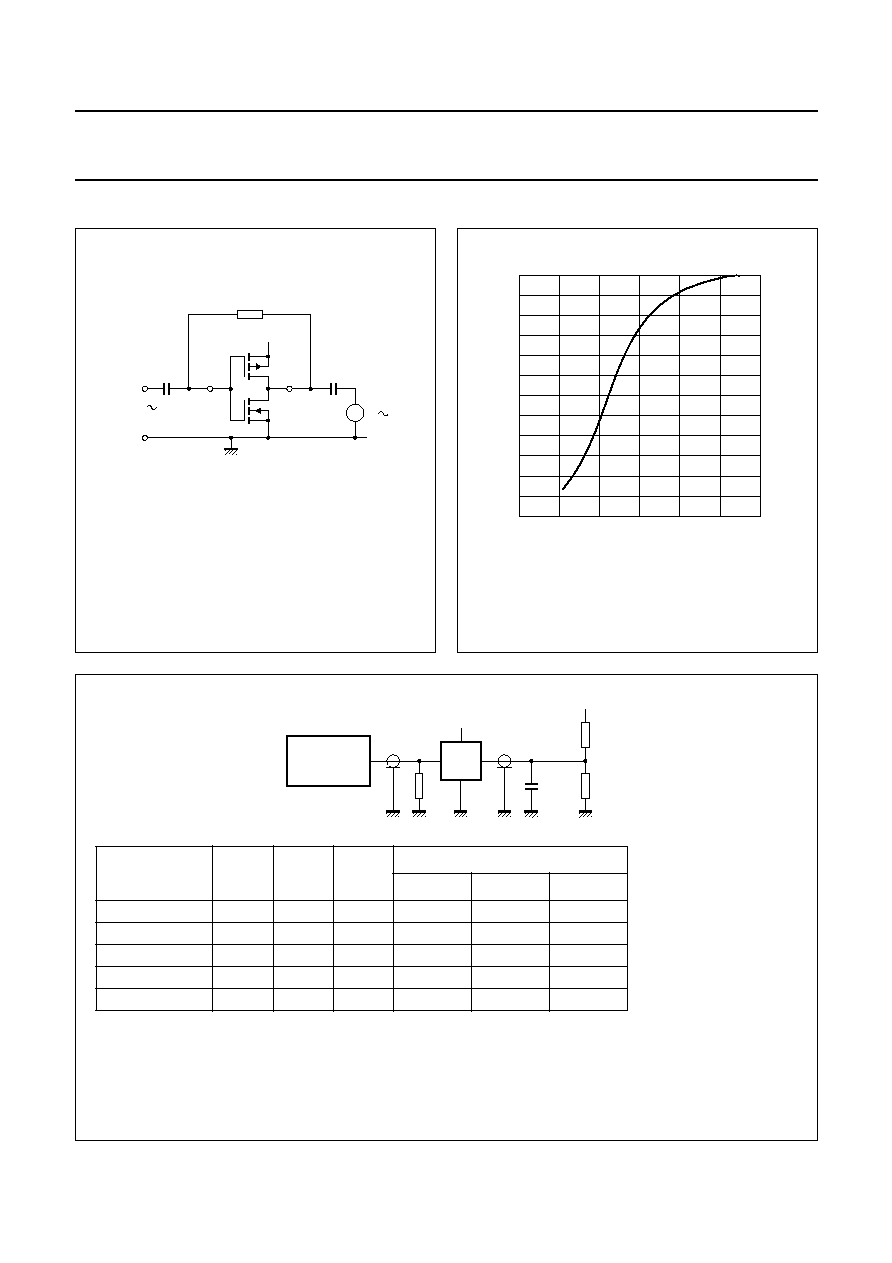
handbook, halfpage
U04
R1
R2
VCC
ZL
MNA052
1
µ
F
Fig.10 Used as a linear amplifier.
Z
L
> 10 k
, R1
3 k
and R2
1 M
.
Open loop amplification: A
OL
= 20 (typical value).
Voltage amplification:
Maximum output voltage:
Unity gain bandwidth product: B = 5 MHz (typical value).
A
u
A
OL
1
R1
R2
-------- 1
A
OL
)
+
(
+
--------------------------------------------
=
V
o(p-p)
V
CC
1.5 V centered at 0.5V
CC
Fig.11 Crystal oscillator configuration.
C1 = 47 pF (typical).
C2 = 22 pF (typical).
R1 = 1 to 10 M
(typical).
R2 optimum value depends on the frequency and required stability
against changes in V
CC
or average minimum I
CC
[I
CC
= 2 mA (typical)
at V
CC
= 3.3 V and f = 10 MHz].
handbook, halfpage
MNA053
U04
out
R2
R1
C1
C2
2004 Sep 21
11
Philips Semiconductors
Product specification
Inverter
74LVC1GU04
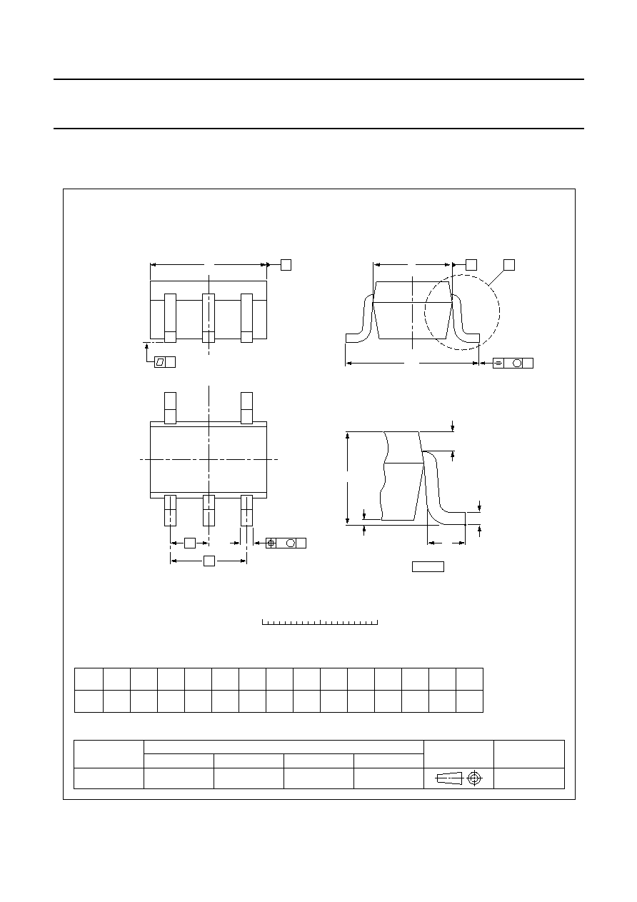
PACKAGE OUTLINES
REFERENCES
OUTLINE
VERSION
EUROPEAN
PROJECTION
ISSUE DATE
IEC
JEDEC
EIAJ
SOT353
w
B
M
bp
D
e1
e
A
A1
Lp
Q
detail X
HE
E
v
M
A
A
B
y
0
1
2 mm
scale
c
X
1
3
2
4
5
Plastic surface mounted package; 5 leads
SOT353
UNIT
A1
max
bp
c
D
E
(2)
e
1
HE
Lp
Q
y
w
v
mm
0.1
0.30
0.20
2.2
1.8
0.25
0.10
1.35
1.15
0.65
e
1.3
2.2
2.0
0.2
0.1
0.2
DIMENSIONS (mm are the original dimensions)
0.45
0.15
0.25
0.15
A
1.1
0.8
97-02-28
SC-88A
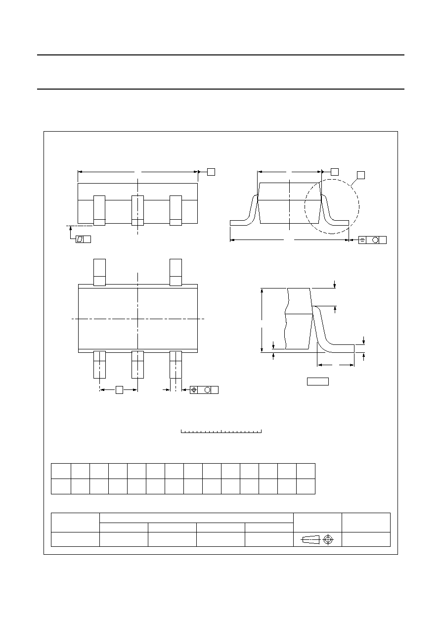
2004 Sep 21
12
Philips Semiconductors
Product specification
Inverter
74LVC1GU04
REFERENCES
OUTLINE
VERSION
EUROPEAN
PROJECTION
ISSUE DATE
IEC
JEDEC
JEITA
SOT753
SC-74A
w
B
M
bp
D
e
A
A1
Lp
Q
detail X
HE
E
v
M
A
A
B
y
0
1
2 mm
scale
c
X
1
3
2
4
5
Plastic surface mounted package; 5 leads
SOT753
UNIT
A1
bp
c
D
E
HE
Lp
Q
y
w
v
mm
0.100
0.013
0.40
0.25
3.1
2.7
0.26
0.10
1.7
1.3
e
0.95
3.0
2.5
0.2
0.1
0.2
DIMENSIONS (mm are the original dimensions)
0.6
0.2
0.33
0.23
A
1.1
0.9
02-04-16
2004 Sep 21
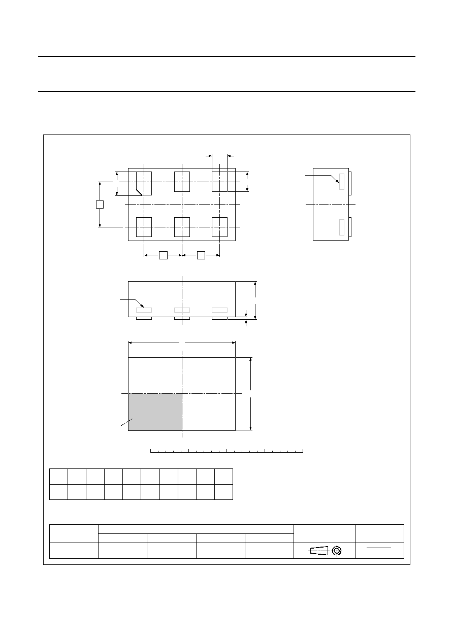
13
Philips Semiconductors
Product specification
Inverter
74LVC1GU04
terminal 1
index area
REFERENCES
OUTLINE
VERSION
EUROPEAN
PROJECTION
ISSUE DATE
IEC
JEDEC
JEITA
SOT886
MO-252
SOT886
04-07-15
04-07-22
DIMENSIONS (mm are the original dimensions)
XSON6: plastic extremely thin small outline package; no leads; 6 terminals; body 1 x 1.45 x 0.5 mm
D
E
e
1
e
A
1
b
L
L
1
e
1
0
1
2 mm
scale
Notes
1. Including plating thickness.
2. Can be visible in some manufacturing processes.
UNIT
mm
0.25
0.17
1.5
1.4
0.35
0.27
A
1
max
b
E
1.05
0.95
D
e
e
1
L
0.40
0.32
L
1
0.5
0.6
A
(1)
max
0.5
0.04
1
6
2
5
3
4
6
×
(2)
4
×
(2)
A
2004 Sep 21
14
Philips Semiconductors
Product specification
Inverter
74LVC1GU04
DATA SHEET STATUS
Notes
1. Please consult the most recently issued data sheet before initiating or completing a design.
2. The product status of the device(s) described in this data sheet may have changed since this data sheet was
published. The latest information is available on the Internet at URL http://www.semiconductors.philips.com.
3. For data sheets describing multiple type numbers, the highest-level product status determines the data sheet status.
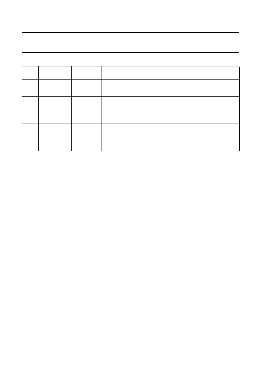
LEVEL
DATA SHEET
STATUS
(1)
PRODUCT
STATUS
(2)(3)
DEFINITION
I
Objective data
Development
This data sheet contains data from the objective specification for product
development. Philips Semiconductors reserves the right to change the
specification in any manner without notice.
II
Preliminary data Qualification
This data sheet contains data from the preliminary specification.
Supplementary data will be published at a later date. Philips
Semiconductors reserves the right to change the specification without
notice, in order to improve the design and supply the best possible
product.
III
Product data
Production
This data sheet contains data from the product specification. Philips
Semiconductors reserves the right to make changes at any time in order
to improve the design, manufacturing and supply. Relevant changes will
be communicated via a Customer Product/Process Change Notification
(CPCN).
DEFINITIONS
Short-form specification
The data in a short-form
specification is extracted from a full data sheet with the
same type number and title. For detailed information see
the relevant data sheet or data handbook.
Limiting values definition
Limiting values given are in
accordance with the Absolute Maximum Rating System
(IEC 60134). Stress above one or more of the limiting
values may cause permanent damage to the device.
These are stress ratings only and operation of the device
at these or at any other conditions above those given in the
Characteristics sections of the specification is not implied.
Exposure to limiting values for extended periods may
affect device reliability.
Application information
Applications that are
described herein for any of these products are for
illustrative purposes only. Philips Semiconductors make
no representation or warranty that such applications will be
suitable for the specified use without further testing or
modification.
DISCLAIMERS
Life support applications
These products are not
designed for use in life support appliances, devices, or
systems where malfunction of these products can
reasonably be expected to result in personal injury. Philips
Semiconductors customers using or selling these products
for use in such applications do so at their own risk and
agree to fully indemnify Philips Semiconductors for any
damages resulting from such application.
Right to make changes
Philips Semiconductors
reserves the right to make changes in the products -
including circuits, standard cells, and/or software -
described or contained herein in order to improve design
and/or performance. When the product is in full production
(status `Production'), relevant changes will be
communicated via a Customer Product/Process Change
Notification (CPCN). Philips Semiconductors assumes no
responsibility or liability for the use of any of these
products, conveys no licence or title under any patent,
copyright, or mask work right to these products, and
makes no representations or warranties that these
products are free from patent, copyright, or mask work
right infringement, unless otherwise specified.

© Koninklijke Philips Electronics N.V. 2004
SCA76
All rights are reserved. Reproduction in whole or in part is prohibited without the prior written consent of the copyright owner.
The information presented in this document does not form part of any quotation or contract, is believed to be accurate and reliable and may be changed
without notice. No liability will be accepted by the publisher for any consequence of its use. Publication thereof does not convey nor imply any license
under patent- or other industrial or intellectual property rights.
Philips Semiconductors a worldwide company
Contact information
For additional information please visit http://www.semiconductors.philips.com.
Fax: +31 40 27 24825
For sales offices addresses send e-mail to: sales.addresses@www.semiconductors.philips.com.
Printed in The Netherlands
R20/06/pp
15
Date of release:
2004 Sep 21
Document order number:
9397 750 13769
Document Outline