2003 Aug 13
2
Philips Semiconductors
Product specification
X-tal driver
74LVC1GX04
FEATURES
∑
Wide supply voltage range from 1.65 to 5.5 V
∑
5 V tolerant input and a 5 V overvoltage tolerant
powered down output.
∑
High noise immunity
∑
Complies with JEDEC standard:
≠ JESD8-7 (1.65 to 1.95 V)
≠ JESD8-5 (2.3 to 2.7 V)
≠ JESD8B/JESD36 (2.7 to 3.6 V).
∑ ±
24 mA output drive (V
CC
= 3.0 V)
∑
CMOS low power consumption
∑
Latch-up performance exceeds 250 mA
∑
Direct interface with TTL levels
∑
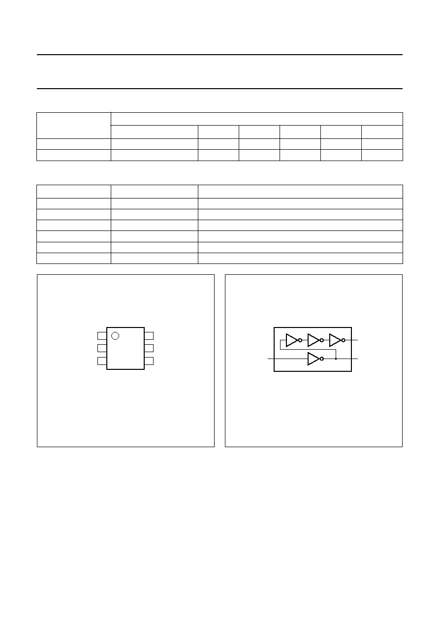
SOT363 and SOT457 package
∑
ESD protection:
≠ HBM EIA/JESD22-A114-A exceeds 2000 V
≠ MM EIA/JESD22-A115-A exceeds 200 V.
∑
Specified from
-
40 to +85
∞
C and
-
40 to +125
∞
C.
DESCRIPTION
The 74LVC1GX04 is a high-performance, low-power,
low-voltage, Si-gate CMOS device and superior to most
advanced CMOS compatible TTL families.
Inputs can be driven from either 3.3 or 5 V devices. This
feature allows the use of this device as translator in a
mixed 3.3 and 5 V environment.
This device is fully specified for partial power-down
applications using I
off
at output Y. The I
off
circuitry disables
the output Y, preventing the damaging backflow current
through the device when it is powered down.
The 74LVC1GX04 combines the functions of the
74LVC1GU04 and 74LVC1G04 to provide a device
optimized for use in crystal oscillator applications.
The integration of the two devices into the 74LVC1GX04
produces the benefits of a compact footprint, lower power
dissipation and stable operation over a wide range of
frequency and temperature.
2003 Aug 13
3
Philips Semiconductors
Product specification
X-tal driver
74LVC1GX04
QUICK REFERENCE DATA
GND = 0 V; T
amb
= 25
∞
C.
Notes
1. C
PD
is used to determine the dynamic power dissipation (P
D
in
µ
W).
P
D
= C
PD
◊
V
CC
2
◊
f
i
◊
N +
(C
L
◊
V
CC
2
◊
f
o
) where:
f
i
= input frequency in MHz;
f
o
= output frequency in MHz;
C
L
= output load capacitance in pF;
V
CC
= supply voltage in Volts;
N = total load switching outputs;
(C
L
◊
V
CC
2
◊
f
o
) = sum of outputs.
2. The condition is V
I
= GND to V
CC
.
FUNCTION TABLE
See note 1.
Note
1. H = HIGH voltage level;
L = LOW voltage level.
SYMBOL
PARAMETER
CONDITIONS
TYPICAL
UNIT
t
PHL
/t
PLH
propagation delay input X1 to output X2
V
CC
= 1.8 V; C
L
= 30 pF; R
L
= 1 k
2.1
ns
V
CC
= 2.5 V; C
L
= 30 pF; R
L
= 500
1.7
ns
V
CC
= 2.7 V; C
L
= 50 pF; R
L
= 500
2.5
ns
V
CC
= 3.3 V; C
L
= 50 pF; R
L
= 500
2.1
ns
V
CC
= 5.0 V; C
L
= 50 pF; R
L
= 500
1.6
ns
propagation delay input X1 to output Y
V
CC
= 1.8 V; C
L
= 30 pF; R
L
= 1 k
4.4
ns
V
CC
= 2.5 V; C
L
= 30 pF; R
L
= 500
2.9
ns
V
CC
= 2.7 V; C
L
= 50 pF; R
L
= 500
3.0
ns
V
CC
= 3.3 V; C
L
= 50 pF; R
L
= 500
2.8
ns
V
CC
= 5.0 V; C
L
= 50 pF; R
L
= 500
2.3
ns
C
I
input capacitance
5
pF
C
PD
power dissipation capacitance per buffer
output enabled; notes 1 and 2
35
pF
INPUT
OUTPUT
X1
X2
Y
H
L
H
L
H
L
2003 Aug 13
5
Philips Semiconductors
Product specification
X-tal driver
74LVC1GX04
RECOMMENDED OPERATING CONDITIONS
Notes
1. For use of a regular crystal oscillator, the recommended minimum V
CC
should be 2.0 V.
2. Only for output Y.
LIMITING VALUES
In accordance with the Absolute Maximum Rating System (IEC 60134); voltages are referenced to GND (ground = 0 V).
Notes
1. The input and output voltage ratings may be exceeded if the input and output current ratings are observed.
2. When V
CC
= 0 V (Power-down mode), the output voltage can be 5.5 V in normal operation.
SYMBOL
PARAMETER
CONDITIONS
MIN.
MAX.
UNIT
V
CC
supply voltage
note 1
1.65
5.5
V
V
I
input voltage
0
5.5
V
V
O
output voltage
note 2
active mode
0
V
CC
V
Power-down mode; V
CC
= 0 V
0
5.5
V
T
amb
operating ambient temperature
-
40
+125
∞
C
t
r
, t
f
input rise and fall times
V
CC
= 1.65 to 2.7 V
0
20
ns/V
V
CC
= 2.7 to 5.5 V
0
10
ns/V
SYMBOL
PARAMETER
CONDITIONS
MIN.
MAX.
UNIT
V
CC
supply voltage
-
0.5
+6.5
V
I
IK
input diode current
V
I
< 0
-
-
50
mA
V
I
input voltage
note 1
-
0.5
+6.5
V
I
OK
output diode current
V
O
> V
CC
or V
O
< 0
-
±
50
mA
V
O
output voltage
active mode; notes 1 and 2
-
0.5
V
CC
+ 0.5
V
Power-down mode; notes 1 and 2
-
0.5
+6.5
V
I
O
output source or sink current
V
O
= 0 to V
CC
-
±
50
mA
I
CC
, I
GND
V
CC
or GND current
-
±
100
mA
T
stg
storage temperature
-
65
+150
∞
C
P
D
power dissipation
T
amb
=
-
40 to +125
∞
C
-
300
mW