2004 Sep 22
2
Philips Semiconductors
Product specification
Dual bus buffer/line driver; 3-state
74LVC2G125
FEATURES
∑
Wide supply voltage range from 1.65 V to 5.5 V
∑
5 V tolerant input/output for interfacing with 5 V logic
∑
High noise immunity
∑
Complies with JEDEC standard:
≠ JESD8-7 (1.65 V to 1.95 V)
≠ JESD8-5 (2.3 V to 2.7 V)
≠ JESD8B/JESD36 (2.7 V to 3.6 V).
∑
ESD protection:
≠ HBM EIA/JESD22-A114-B exceeds 2000 V
≠ MM EIA/JESD22-A115-A exceeds 200 V.
∑ ±
24 mA output drive (V
CC
= 3.0 V)
∑
CMOS low power consumption
∑
Latch-up performance exceeds 250 mA
∑
Direct interface with TTL levels
∑
Inputs accept voltages up to 5 V
∑
Multiple package options
∑
Specified from
-
40
∞
C to +85
∞
C and
-
40
∞
C to +125
∞
C.
DESCRIPTION
The 74LVC2G125 is a high-performance, low-power,
low-voltage, Si-gate CMOS device and superior to most
advanced CMOS compatible TTL families.
Inputs can be driven from either 3.3 V or 5 V devices.
This feature allows the use of these devices as translators
in a mixed 3.3 V and 5 V environment.
This device is fully specified for partial power-down
applications using I
off
. The I
off
circuitry disables the output,
preventing the damaging backflow current through the
device when it is powered down.
The 74LVC2G125 provides a dual non-inverting buffer/line
driver with 3-state output. The 3-state output is controlled
by the output enable input (pin nOE). A HIGH-level at
pin nOE causes the output to assume a high-impedance
OFF-state. Schmitt-trigger action at all inputs makes the
circuit highly tolerant for slower input rise and fall times.
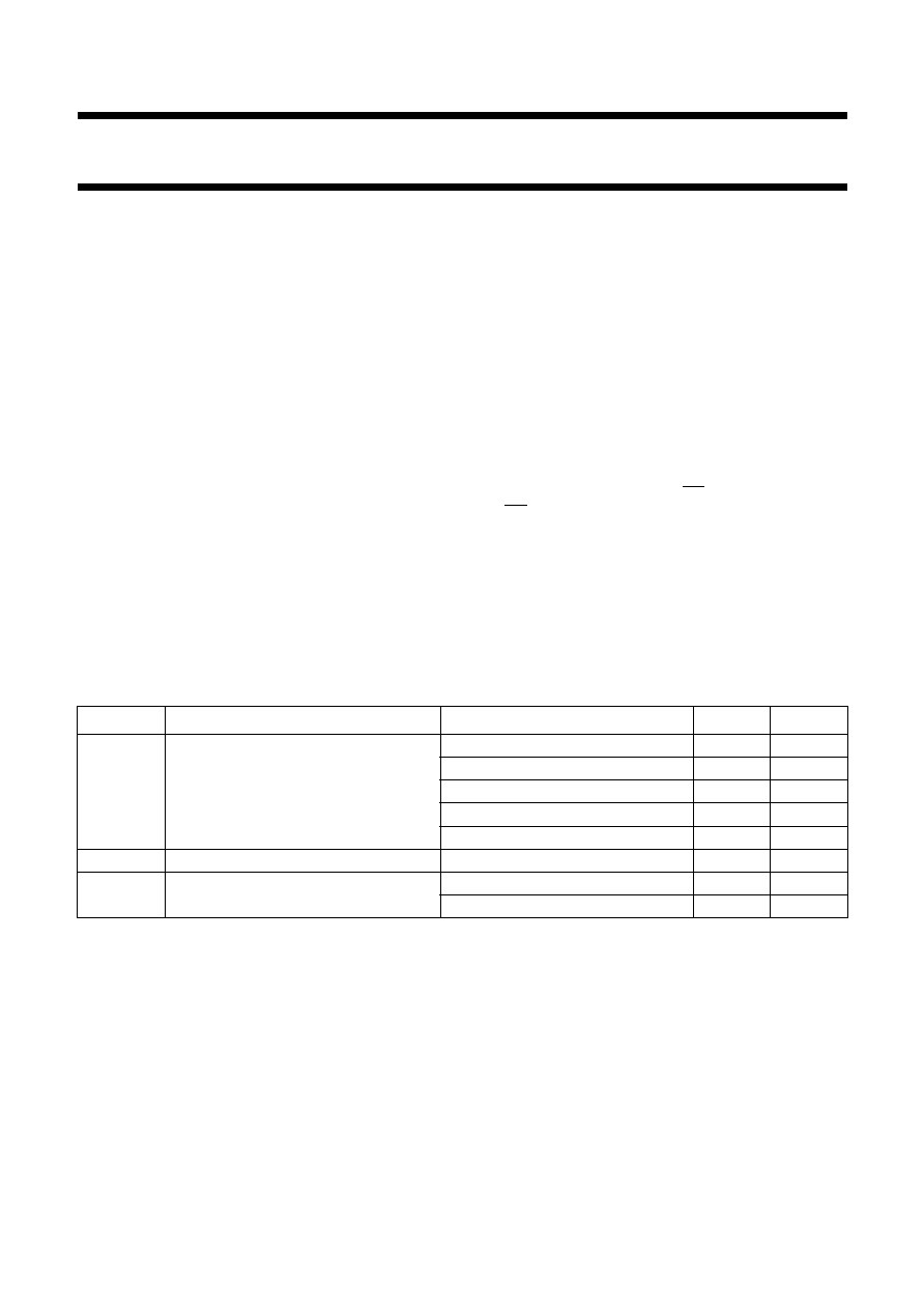
QUICK REFERENCE DATA
GND = 0 V; T
amb
= 25
∞
C.
Notes
1. C
PD
is used to determine the dynamic power dissipation (P
D
in
µ
W).
P
D
= C
PD
◊
V
CC
2
◊
f
i
◊
N +
(C
L
◊
V
CC
2
◊
f
o
) where:
f
i
= input frequency in MHz;
f
o
= output frequency in MHz;
C
L
= output load capacitance in pF;
V
CC
= supply voltage in Volts;
N = total load switching outputs;
(C
L
◊
V
CC
2
◊
f
o
) = sum of outputs.
2. The condition is V
I
= GND to V
CC
.
SYMBOL
PARAMETER
CONDITIONS
TYPICAL
UNIT
t
PHL
/t
PLH
propagation delay inputs nA to output nY V
CC
= 1.8 V; C
L
= 30 pF; R
L
= 1 k
3.7
ns
V
CC
= 2.5 V; C
L
= 30 pF; R
L
= 500
2.5
ns
V
CC
= 2.7 V; C
L
= 50 pF; R
L
= 500
2.7
ns
V
CC
= 3.3 V; C
L
= 50 pF; R
L
= 500
2.3
ns
V
CC
= 5.0 V; C
L
= 50 pF; R
L
= 500
1.9
ns
C
I
input capacitance
2
pF
C
PD
power dissipation capacitance per buffer
output enabled; notes 1 and 2
18
pF
output disabled; notes 1 and 2
5
pF
2004 Sep 22
3
Philips Semiconductors
Product specification
Dual bus buffer/line driver; 3-state
74LVC2G125
FUNCTION TABLE
See note 1.
Note
1. H = HIGH voltage level;
L = LOW voltage level;
X = don't care;
Z = high-impedance OFF-state.
ORDERING INFORMATION
PINNING
INPUT
OUTPUT
nOE
nA
nY
L
L
L
L
H
H
H
X
Z
TYPE NUMBER
PACKAGE
TEMPERATURE
RANGE
PINS
PACKAGE
MATERIAL
CODE
MARKING
74LVC2G125DP
-
40
∞
C to +125
∞
C
8
TSSOP8
plastic
SOT505-2
V125
74LVC2G125DC
-
40
∞
C to +125
∞
C
8
VSSOP8
plastic
SOT765-1
V25
74LVC2G125GM
-
40
∞
C to +125
∞
C
8
XSON8
plastic
SOT833-1
V25
PIN
SYMBOL
DESCRIPTION
1
1OE
output enable input (active LOW)
2
1A
data input
3
2Y
data output
4
GND
ground (0 V)
5
2A
data input
6
1Y
data output
7
2OE
output enable input (active LOW)
8
V
CC
supply voltage

2004 Sep 22
5
Philips Semiconductors
Product specification
Dual bus buffer/line driver; 3-state
74LVC2G125
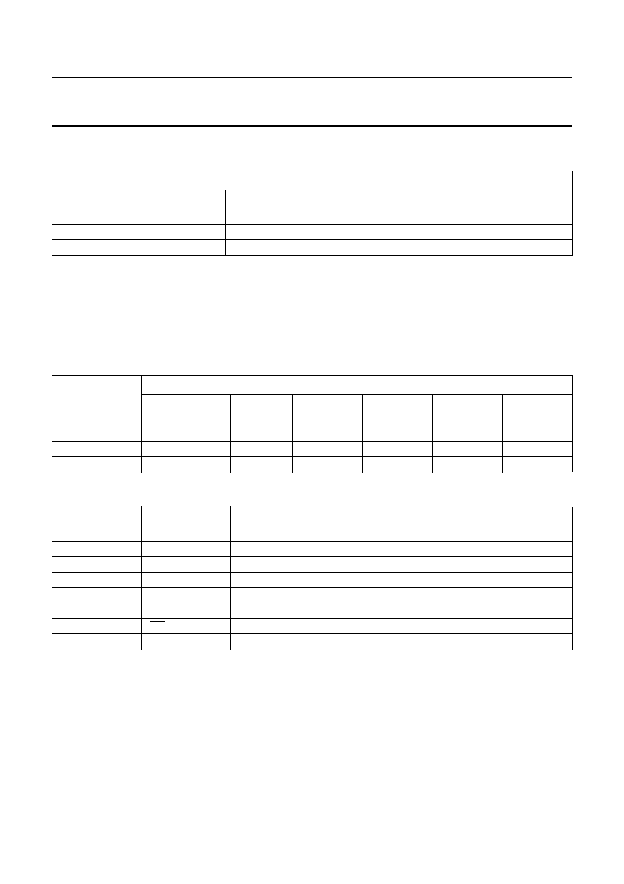
RECOMMENDED OPERATING CONDITIONS
LIMITING VALUES
In accordance with the Absolute Maximum Rating System (IEC 60134); voltages are referenced to GND (ground = 0 V).
Notes
1. The input and output voltage ratings may be exceeded if the input and output current ratings are observed.
2. When V
CC
= 0 V (Power-down mode), the output voltage can be 5.5 V in normal operation.
SYMBOL
PARAMETER
CONDITIONS
MIN.
MAX.
UNIT
V
CC
supply voltage
1.65
5.5
V
V
I
input voltage
0
5.5
V
V
O
output voltage
V
CC
= 1.65 V to 5.5 V; enable
mode
0
V
CC
V
V
CC
= 1.65 V to 5.5 V; disable
mode
0
5.5
V
V
CC
= 0 V; Power-down mode
0
5.5
V
T
amb
operating ambient temperature
-
40
+125
∞
C
t
r
, t
f
input rise and fall times
V
CC
= 1.65 V to 2.7 V
0
20
ns/V
V
CC
= 2.7 V to 5.5 V
0
10
ns/V
SYMBOL
PARAMETER
CONDITIONS
MIN.
MAX.
UNIT
V
CC
supply voltage
-
0.5
+6.5
V
I
IK
input diode current
V
I
< 0 V
-
-
50
mA
V
I
input voltage
note 1
-
0.5
+6.5
V
I
OK
output diode current
V
O
> V
CC
or V
O
< 0 V
-
±
50
mA
V
O
output voltage
enable mode; notes 1 and 2
-
0.5
V
CC
+ 0.5
V
disable mode; notes 1 and 2
-
0.5
+6.5
V
Power-down mode; notes 1 and 2
-
0.5
+6.5
V
I
O
output source or sink current
V
O
= 0 V to V
CC
-
±
50
mA
I
CC
, I
GND
V
CC
or GND current
-
±
100
mA
T
stg
storage temperature
-
65
+150
∞
C
P
tot
power dissipation
T
amb
=
-
40
∞
C to +125
∞
C
-
300
mW