2004 Oct 18
2
Philips Semiconductors
Product specification
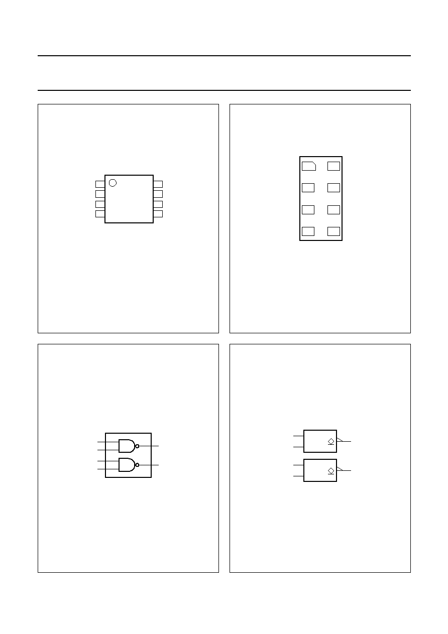
Dual 2-input NAND gate (open drain)
74LVC2G38
FEATURES
∑
Wide supply voltage range from 1.65 V to 5.5 V
∑
5 V tolerant outputs for interfacing with 5 V logic
∑
High noise immunity
∑
Complies with JEDEC standard:
≠ JESD8-7 (1.65 V to 1.95 V)
≠ JESD8-5 (2.3 V to 2.7 V)
≠ JESD8B/JESD36 (2.7 V to 3.6 V).
∑
ESD protection:
≠ HBM EIA/JESD22-A114-B exceeds 2000 V
≠ MM EIA/JESD22-A115-A exceeds 200 V.
∑ ±
24 mA output drive (V
CC
= 3.0 V)
∑
CMOS low power consumption
∑
Open drain outputs
∑
Latch-up performance exceeds 250 mA
∑
Direct interface with TTL levels
∑
Inputs accept voltages up to 5 V
∑
Multiple package options
∑
Specified from
-
40
∞
C to +85
∞
C and
-
40
∞
C to +125
∞
C.
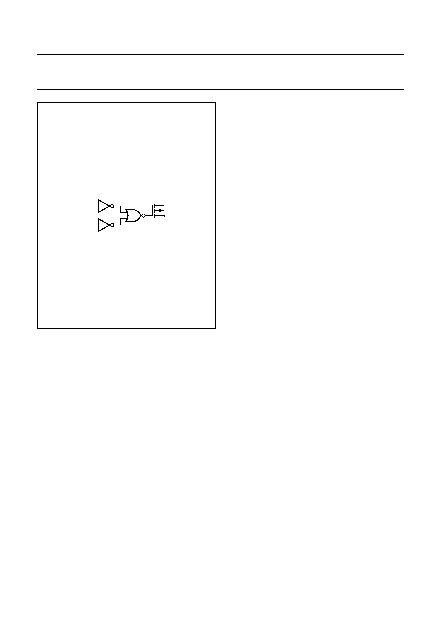
DESCRIPTION
The 74LVC2G38 is a high-performance, low-power,
low-voltage, Si-gate CMOS device and superior to most
advanced CMOS compatible TTL families.
Inputs can be driven from either 3.3 V or 5 V devices.
These feature allows the use of these devices as
translators in a mixed 3.3 V and 5 V environment.
This device is fully specified for partial power-down
applications using I
off
. The I
off
circuitry disables the output,
preventing the damaging backflow current through the
device when it is powered down.
The 74LVC2G38 provides the 2-input NAND function.
The outputs of the 74LVC2G38 devices are open drain
and can be connected to other open-drain outputs to
implement active-LOW, wired-OR or active-HIGH
wired-AND functions.
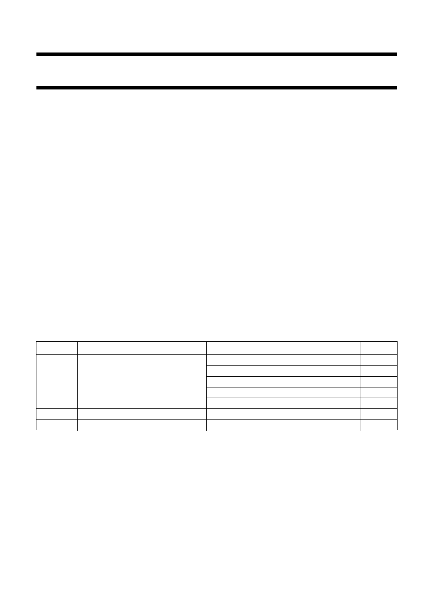
QUICK REFERENCE DATA
GND = 0 V; T
amb
= 25
∞
C.
Notes
1. C
PD
is used to determine the dynamic power dissipation (P
D
in
µ
W).
P
D
= C
PD
◊
V
CC
2
◊
f
i
◊
N +
(C
L
◊
V
CC
2
◊
f
o
) where:
f
i
= input frequency in MHz;
f
o
= output frequency in MHz;
C
L
= output load capacitance in pF;
V
CC
= supply voltage in Volts;
N = number of inputs switching;
(C
L
◊
V
CC
2
◊
f
o
) = sum of outputs.
2. The condition is V
I
= GND to V
CC
.
SYMBOL
PARAMETER
CONDITIONS
TYPICAL
UNIT
t
PZL
/t
PLZ
propagation delay inputs nA and nB to
output nY
V
CC
= 1.8 V; C
L
= 30 pF; R
L
= 1 k
3.0
ns
V
CC
= 2.5 V; C
L
= 30 pF; R
L
= 500
1.8
ns
V
CC
= 2.7 V; C
L
= 50 pF; R
L
= 500
2.5
ns
V
CC
= 3.3 V; C
L
= 50 pF; R
L
= 500
2.1
ns
V
CC
= 5.0 V; C
L
= 50 pF; R
L
= 500
1.5
ns
C
I
input capacitance
2.5
pF
C
PD
power dissipation capacitance per gate
V
CC
= 3.3 V; notes 1 and 2
5
pF