2004 Sep 21
2
Philips Semiconductors
Product specification
Dual inverter
74LVC2GU04
FEATURES
·
Wide supply voltage range from 1.65 V to 5.5 V
·
5 V tolerant input/output for interfacing with 5 V logic
·
High noise immunity
·
ESD protection:
HBM EIA/JESD22-A114-B exceeds 2000 V
MM EIA/JESD22-A115-A exceeds 200 V.
· ±
24 mA output drive (V
CC
= 3.0 V)
·
CMOS low power consumption
·
Latch-up performance exceeds 250 mA
·
Multiple package options
·
Specified from
-
40
°
C to +85
°
C and
-
40
°
C to +125
°
C.
DESCRIPTION
The 74LVC2GU04 is a high-performance, low-power,
low-voltage, Si-gate CMOS device, superior to most
advanced CMOS compatible TTL families.
Input can be driven from either 3.3 V or 5 V devices.
These features allow the use of these devices in a mixed
3.3 V and 5 V environment.
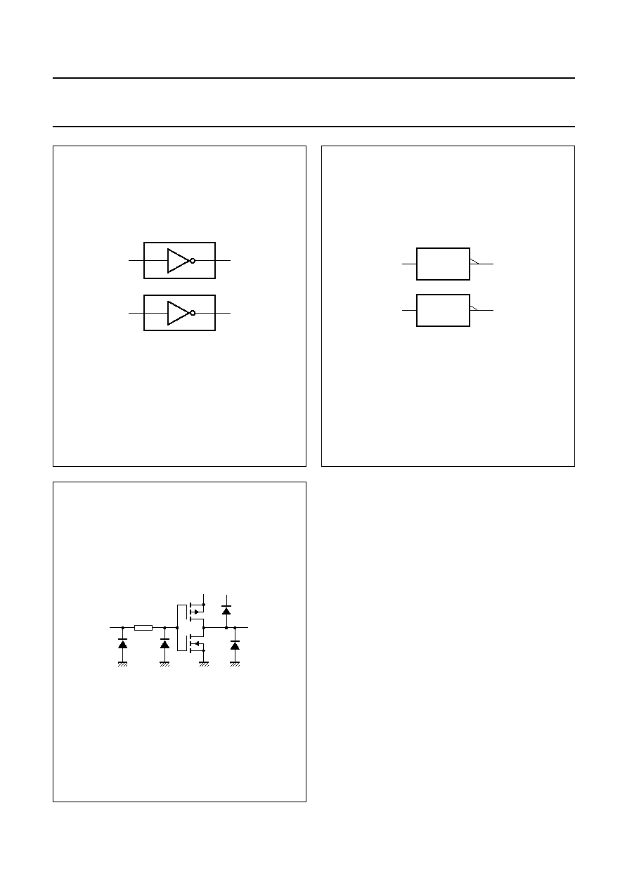
The 74LVC2GU04 provides two inverters. Each inverter is
a single stage with unbuffered output.
QUICK REFERENCE DATA
GND = 0 V; T
amb
= 25
°
C.
Notes
1. C
PD
is used to determine the dynamic power dissipation (P
D
in
µ
W).
P
D
= C
PD
×
V
CC
2
×
f
i
×
N +
(C
L
×
V
CC
2
×
f
o
) where:
f
i
= input frequency in MHz;
f
o
= output frequency in MHz;
C
L
= output load capacitance in pF;
V
CC
= supply voltage in Volts;
N = total load switching outputs;
(C
L
×
V
CC
2
×
f
o
) = sum of outputs.
2. The condition is V
I
= GND to V
CC
.
SYMBOL
PARAMETER
CONDITIONS
TYPICAL
UNIT
t
PHL
/t
PLH
propagation delay input nA to output nY
V
CC
= 1.8 V; C
L
= 30 pF; R
L
= 1 k
2.3
ns
V
CC
= 2.5 V; C
L
= 30 pF; R
L
= 500
1.8
ns
V
CC
= 2.7 V; C
L
= 50 pF; R
L
= 500
2.6
ns
V
CC
= 3.3 V; C
L
= 50 pF; R
L
= 500
2.3
ns
V
CC
= 5.0 V; C
L
= 50 pF; R
L
= 500
1.7
ns
C
I
input capacitance
5
pF
C
PD
power dissipation capacitance per gate
V
CC
= 3.3 V; notes 1 and 2
7.8
pF
2004 Sep 21
3
Philips Semiconductors
Product specification
Dual inverter
74LVC2GU04
FUNCTION TABLE
See note 1.
Note
1. H = HIGH voltage level;
L = LOW voltage level.
ORDERING INFORMATION
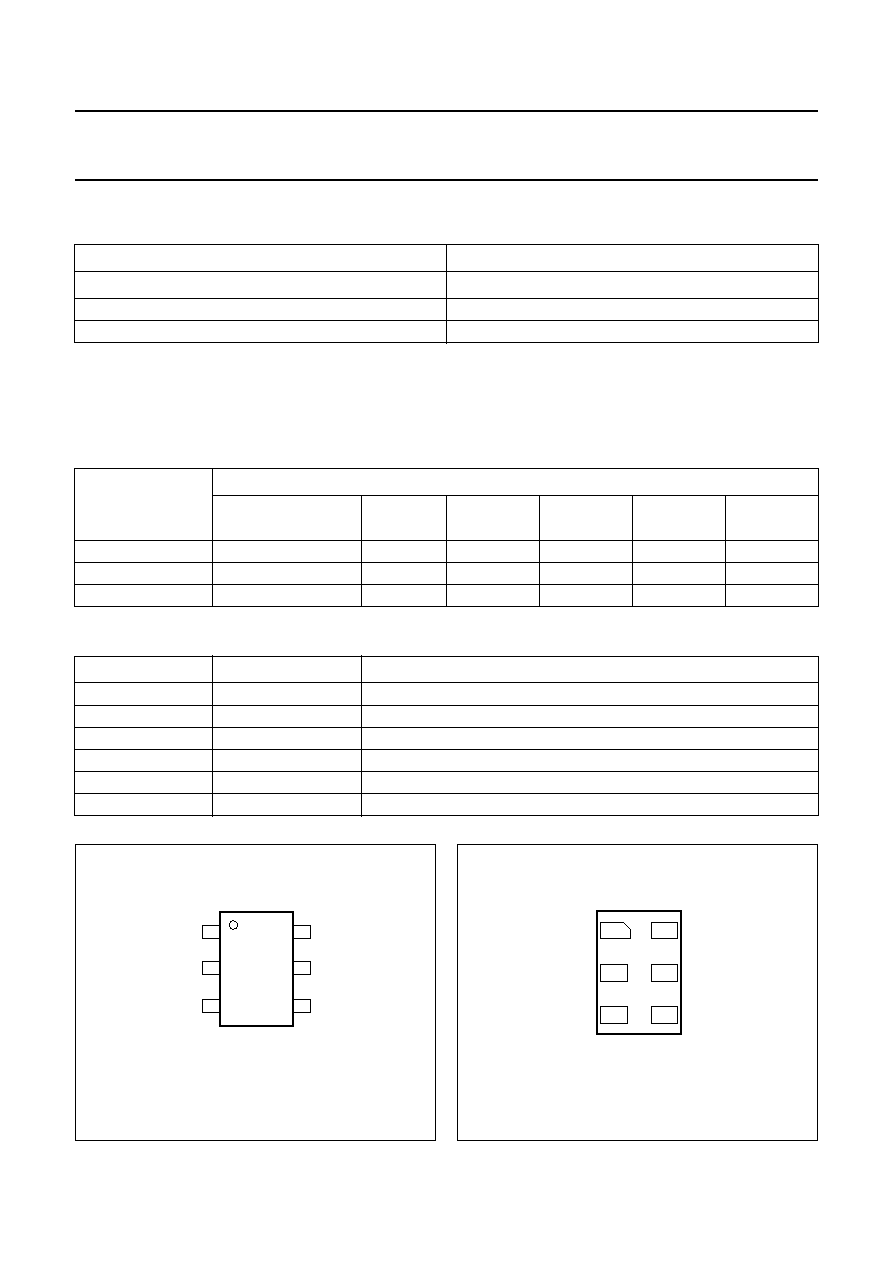
PINNING
INPUT
OUTPUT
nA
nY
L
H
H
L
TYPE NUMBER
PACKAGE
TEMPERATURE
RANGE
PINS
PACKAGE
MATERIAL
CODE
MARKING
74LVC2GU04GW
-
40
°
C to +125
°
C
6
SC-88
plastic
SOT363
YD
74LVC2GU04GV
-
40
°
C to +125
°
C
6
SC-74
plastic
SOT457
VU4
74LVC2GU04GM
-
40
°
C to +125
°
C
6
XSON6
plastic
SOT886
YD
PIN
SYMBOL
DESCRIPTION
1
1A
data input
2
GND
ground (0 V)
3
2A
data input
4
2Y
data output
5
V
CC
supply voltage
6
1Y
data output
U04
1A
1Y
GND
2A
2Y
001aab680
1
2
3
6
V
CC
5
4
Fig.1 Pin configuration SC-88 and SC-74.
04
GND
001aab681
1A
2A
V
CC
1Y
2Y
Transparent top view
2
3
1
5
4
6
Fig.2 Pin configuration XSON6.
2004 Sep 21
5
Philips Semiconductors
Product specification
Dual inverter
74LVC2GU04
RECOMMENDED OPERATING CONDITIONS
LIMITING VALUES
In accordance with the Absolute Maximum Rating System (IEC 60134); voltages are referenced to GND (ground = 0 V).
Note
1. The input and output voltage ratings may be exceeded if the input and output current ratings are observed.
SYMBOL
PARAMETER
CONDITIONS
MIN.
MAX.
UNIT
V
CC
supply voltage
1.65
5.5
V
V
I
input voltage
0
5.5
V
V
O
output voltage
active mode
0
V
CC
V
T
amb
operating ambient temperature
-
40
+125
°
C
t
r
, t
f
input rise and fall times
V
CC
= 1.65 V to 2.7 V
0
20
ns/V
V
CC
= 2.7 V to 5.5 V
0
10
ns/V
SYMBOL
PARAMETER
CONDITIONS
MIN.
MAX.
UNIT
V
CC
supply voltage
-
0.5
+6.5
V
I
IK
input diode current
V
I
< 0 V
-
-
50
mA
V
I
input voltage
note 1
-
0.5
+6.5
V
I
OK
output diode current
V
O
> V
CC
or V
O
< 0 V
-
±
50
mA
V
O
output voltage
active mode; note 1
-
0.5
V
CC
+ 0.5
V
I
O
output source or sink current
V
O
= 0 V to V
CC
-
±
50
mA
I
CC
, I
GND
V
CC
or GND current
-
±
100
mA
T
stg
storage temperature
-
65
+150
°
C
P
tot
power dissipation
T
amb
=
-
40
°
C to +125
°
C
-
300
mW