
Philips
Semiconductors
74LVC543A
Octal D-type registered transceiver
(3-State)
Product specification
Supersedes data of 1997 Jun 30
IC24 Data Handbook
1998 Jul 31
INTEGRATED CIRCUITS
Philips Semiconductors
Product specification
74LVC543A
Octal D-type registered transceiver (3-State)
2
1998 Jul 31
853-1992 19813
FEATURES
∑
5-volt tolerant inputs/outputs, for interfacing with 5-volt logic
∑
Supply voltage range of 1.2V to 3.6V
∑
Complies with JEDEC standard no. 8≠1A
∑
CMOS low power consumption
∑
Direct interface with TTL levels
∑
8-bit octal transceiver with D-type latch
∑
Back-to-back registers for storage
∑
Separate controls for data flow in each direction
∑
3-State non-inverting outputs for bus oriented applications
∑
High impedance when V
CC
= 0V
DESCRIPTION
The 74LVC543A is a high≠performance, low≠power, low≠voltage,
Si≠gate CMOS device and superior to most advanced CMOS
compatible TTL families.
The 74LVC543A is an octal registered transceiver containing two
sets of D≠type latches for temporary storage of the data flow in
either direction. Separate latch enable (LE
AB
, LE
BA
) and output
enable (OE
AB
, OE
BA
) inputs are provided for each register to permit
independent control of inputting and outputting in either direction of
the data flow.
The 74LVC543A contains eight D≠type latches, with separate inputs
and controls for each set. For data flow from A to B, for example, the
A≠to≠B enable (E
AB
) input must be LOW in order to enter data from
A
0
≠A
7
or take data from B
0
≠B
7
, as indicated in the function table.
With E
AB
LOW, a LOW signal on the A≠to≠B latch enable (LE
AB
)
input makes the A≠to≠B latches transparent; a subsequent LOW≠to
HIGH transition of the LE
AB
signal puts the A data into the latches
where it is stored and the B outputs no longer change with the A
inputs. With E
AB
and OE
AB
both low, the 3≠state B output buffers
are active and display the data present at the outputs of the A
latches
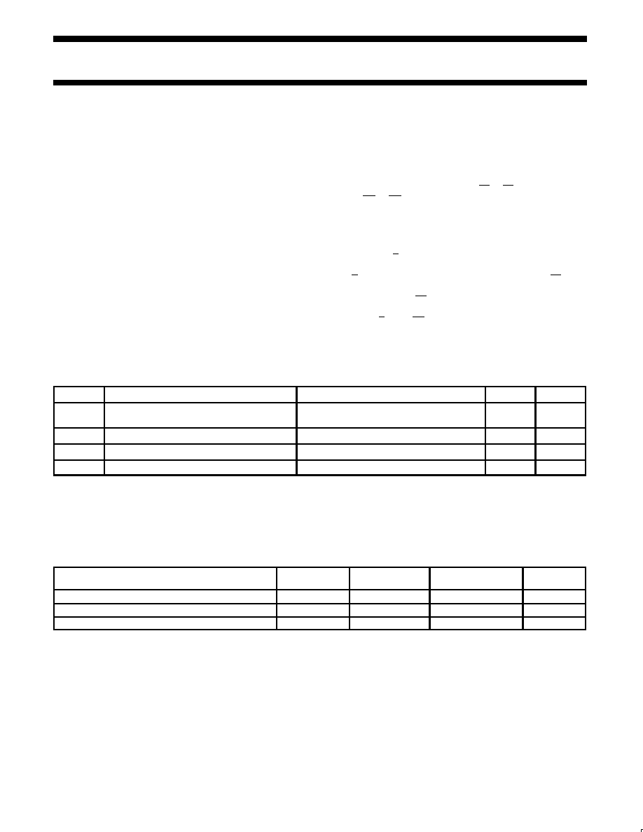
QUICK REFERENCE DATA
GND = 0V; T
amb
= 25
∞
C; T
r
= T
f
2.5ns
SYMBOL
PARAMETER
CONDITIONS
TYPICAL
UNIT
t
PHL
/t
PLH
Propagation delay
A
n
to B
n
C
L
= 50 pF
V
CC
= 3.3V
3.3
ns
C
I
input capacitance
5.0
pF
C
I/O
input/output capacitance
10.0
pF
C
PD
power dissipation capacitance per latch
V
CC
= 3.3V
27
pF
NOTES:
1. C
PD
is used to determine the dynamic power dissipation (P
D
in
µ
W)
P
D
= C
PD
x V
CC
2
x f
i
+
(C
L
x V
CC
2
x f
o )
where:
f
i
= input frequency in MHz; C
L
= output load capacity in pF;
f
o
= output frequency in MHz; V
CC
= supply voltage in V;
(C
L
x V
CC
2
x f
o )
= sum of the outputs
2. The condition is V
I
= GND to V
CC
ORDERING INFORMATION
PACKAGES
TEMPERATURE
RANGE
OUTSIDE NORTH
AMERICA
NORTH AMERICA
PKG DWG. #
24-Pin Plastic Small Outline (SO)
≠40
∞
C to +85
∞
C
74LVC543A D
74LVC543A D
SOT137-1
24-Pin Plastic Shrink Small Outline (SSOP) Type II
≠40
∞
C to +85
∞
C
74LVC543A DB
74LVC543A DB
SOT340-1
24-Pin Plastic Thin Shrink Small Outline (TSSOP) Type I
≠40
∞
C to +85
∞
C
74LVC543A PW
7LVC543APW DH
SOT355-1

Philips Semiconductors
Product specification
74LVC543A
Octal D-type registered transceiver (3-State)
1998 Jul 31
3
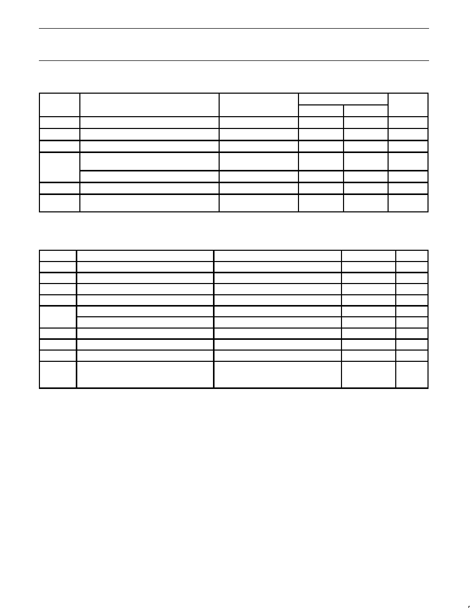
PIN CONFIGURATION
1
2
3
4
5
6
7
8
9
10
11
12
13
14
15
16
17
18
19
20
21
22
23
24
LEBA
OEBA
A0
A1
A2
A3
A4
A5
A6
A7
EBA
VCC
EAB
B0
B1
B2
B3
B4
B6
B5
B7
LEAB
OEAB
GND
SW00212
PIN DESCRIPTION
PIN NUMBER
SYMBOL
FUNCTION
1
LE
BA
'B' to 'A' latch enable input
(active LOW)
2
OE
BA
'B' to 'A' output enable
input (active LOW)
3,4,5,6, 7, 8, 9 10
A
0
to A
7
'A' data inputs/outputs
11
E
BA
'B' to 'A' enable input
(active LOW)
12
GND
ground (0V)
22, 21, 20, 19,
18, 17, 16, 15
B
0
to B
7
'B' data inputs/outputs
13
OE
AB
'A' to 'B' output enable
input (active LOW)
14
LE
AB
'A' to 'B' latch enable input
(active LOW)
23
E
AB
'A' to 'B' enable input
(active LOW)
24
V
CC
positive supply voltage
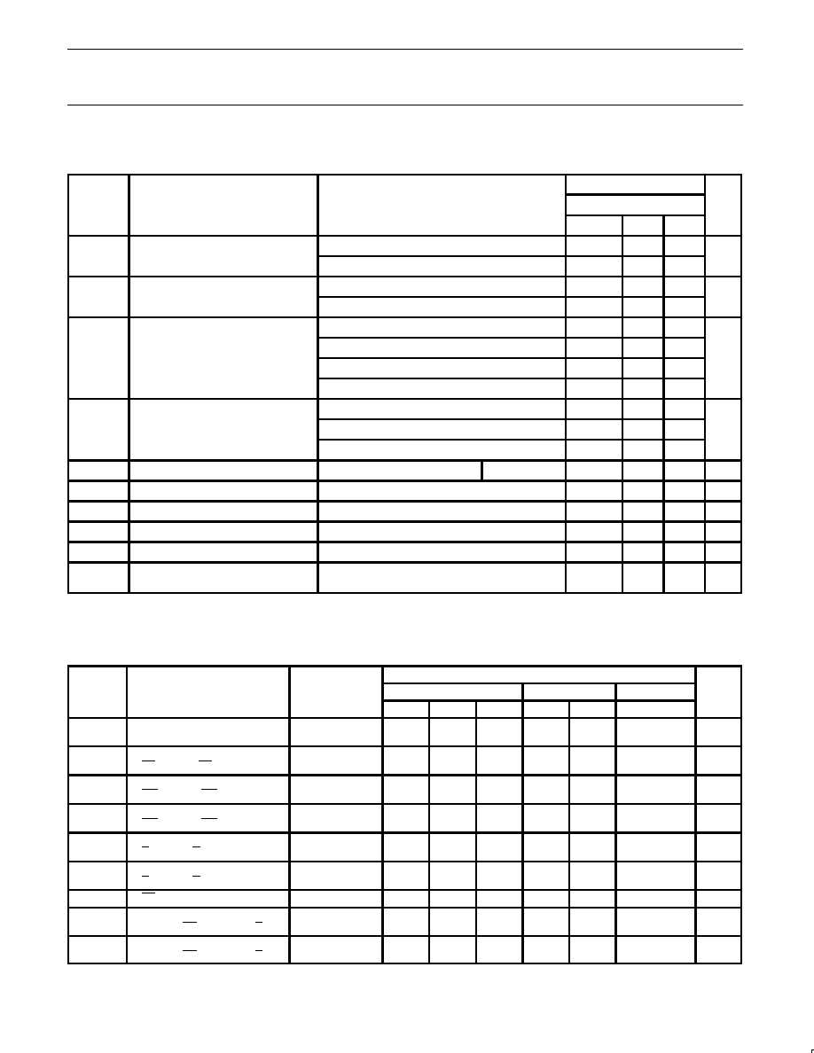
LOGIC SYMBOL
8
9
7
10
4
5
3
6
17
16
18
15
21
20
22
19
B5
B6
B4
B7
B1
B2
B0
B3
1
14
13
11
2
23
A5
A6
A4
A7
A1
A2
A0
A3
LEBA
LEAB
OEAB
EBA
OEBA
EAB
SW00213
LOGIC SYMBOL (IEEE/IEC)
2EN4
13
G2
1
2C6
3
4
3
4
5
6
7
8
9
10
22
21
20
19
18
17
16
15
SW00214
6D
5D
1C5
G1
1EN3
2
23
11
14

Philips Semiconductors
Product specification
74LVC543A
Octal D-type registered transceiver (3-State)
1998 Jul 31
4
LOGIC DIAGRAM
LE
D
LE
D
A
n
B
n
TO 7 OTHER CHANNELS
8 IDENTICAL
CHANNELS
OE
BA
E
BA
LE
BA
OE
AB
E
AB
LE
AB
SW00215
FUNCTION TABLE
OPERATING MODES
INPUTS
OUTPUTS
OPERATING MODES
OE
XX
E
XX
LE
XX
DATA
OUTPUTS
Disabled
H
X
X
X
Z
Disabled
X
H
X
X
Z
Disabled
X
H
X
X
Z
Disabled + Latch
L
L
L
L
h
l
Z
Z
Latch + Display
L
L
L
L
h
l
H
L
Transparent
L
L
L
L
L
L
H
L
H
L
Hold
L
L
H
X
NC
(do nothing)
L
L
H
X
NC
NOTES:
XX =
AB for A-to-B direction, BA for B-to-A direction
H
=
High voltage level
L
=
Low voltage level
h
=
High state must be present one setup time before the Low-to-High transition of LE
AB
, LE
BA
, E
AB
, E
BA
l
=
Low state must be present one setup time before the Low-to-High transition of LE
AB
, LE
BA
, E
AB
, E
BA
X
=
Don't care
=
Low-to-High level transition
NC =
No change
Z
=
High impedance OFF state
Philips Semiconductors
Product specification
74LVC543A
Octal D-type registered transceiver (3-State)
1998 Jul 31
5
RECOMMENDED OPERATING CONDITIONS
SYMBOL
PARAMETER
CONDITIONS
LIMITS
UNIT
SYMBOL
PARAMETER
CONDITIONS
MIN
MAX
UNIT
V
CC
DC supply voltage (for max. speed performance)
2.7
3.6
V
V
CC
DC supply voltage (for low-voltage applications)
1.2
3.6
V
V
I
DC Input voltage range
0
5.5
V
V
I/O
DC Output voltage range; output HIGH or LOW
state
0
V
CC
V
I/O
DC input voltage range; output 3-State
0
5.5
V
T
amb
Operating ambient temperature range in free-air
≠40
+85
∞
C
t
r
, t
f
Input rise and fall times
V
CC
= 1.2 to 2.7V
V
CC
= 2.7 to 3.6V
0
0
20
10
ns/V
ABSOLUTE MAXIMUM RATINGS
1
In accordance with the Absolute Maximum Rating System (IEC 134)
Voltages are referenced to GND (ground = 0V)
SYMBOL
PARAMETER
CONDITIONS
RATING
UNIT
V
CC
DC supply voltage
≠0.5 to +6.5
V
I
IK
DC input diode current
V
I
t
0
≠50
mA
V
I
DC input voltage
Note 2
≠0.5 to +6.5
V
I
OK
DC output diode current
V
O
u
V
CC
or V
O
t
0
"
50
mA
V
I/O
DC output voltage; output HIGH or LOW state
Note 2
≠0.5 to V
CC
+0.5
V
V
I/O
DC input voltage; output 3-State
Note 2
≠0.5 to 6.5
V
I
O
DC output source or sink current
V
O
= 0 to V
CC
"
50
mA
I
GND
, I
CC
DC V
CC
or GND current
"
100
mA
T
stg
Storage temperature range
≠65 to +150
∞
C
Power dissipation per package
P
TOT
≠ plastic mini-pack (SO)
above +70
∞
C derate linearly with 8 mW/K
500
mW
≠ plastic shrink mini-pack (SSOP and TSSOP)
above +60
∞
C derate linearly with 5.5 mW/K
500
mW
NOTES:
1. Stresses beyond those listed may cause permanent damage to the device. These are stress ratings only and functional operation of the
device at these or any other conditions beyond those indicated under "recommended operating conditions" is not implied. Exposure to
absolute-maximum-rated conditions for extended periods may affect device reliability.
2. The input and output voltage ratings may be exceeded if the input and output current ratings are observed.
Philips Semiconductors
Product specification
74LVC543A
Octal D-type registered transceiver (3-State)
1998 Jul 31
6
DC ELECTRICAL CHARACTERISTICS
Over recommended operating conditions voltages are referenced to GND (ground = 0V)
LIMITS
SYMBOL
PARAMETER
TEST CONDITIONS
Temp = -40
∞
C to +85
∞
C
UNIT
MIN
TYP
1
MAX
V
HIGH level Input voltage
V
CC
= 1.2V
V
CC
V
V
IH
HIGH level Input voltage
V
CC
= 2.7 to 3.6V
2.0
V
V
LOW level Input voltage
V
CC
= 1.2V
GND
V
V
IL
LOW level Input voltage
V
CC
= 2.7 to 3.6V
0.8
V
V
CC
= 2.7V; V
I
= V
IH
or V
IL
; I
O
= ≠12mA
V
CC
*
0.5
V
O
HIGH level output voltage
V
CC
= 3.0V; V
I
= V
IH
or V
IL
; I
O
= ≠100
µ
A
V
CC
*
0.2
V
CC
V
V
OH
HIGH level output voltage
V
CC
= 3.0V; V
I
= V
IH
or V
IL;
I
O
= ≠18mA
V
CC
*
0.6
V
V
CC
= 3.0V; V
I
= V
IH
or V
IL;
I
O
= ≠24mA
V
CC
*
0.8
V
CC
= 2.7V; V
I
= V
IH
or V
IL
; I
O
= 12mA
0.40
V
OL
LOW level output voltage
V
CC
= 3.0V; V
I
= V
IH
or V
IL
; I
O
= 100
µ
A
GND
0.20
V
V
CC
= 3.0V; V
I
= V
IH
or V
IL;
I
O
= 24mA
0.55
I
I
Input leakage current
V
CC
= 3.6V; V
I
= 5.5V or GND
Not for I/O pins
"
0.1
"
5
µ
A
I
IHZ
/I
ILZ
Input current for common I/O pins
V
CC
= 3.6V; V
I
= 5.5V or GND
"
0.1
"
15
µ
A
I
OZ
3-State output OFF-state current
V
CC
= 3.6V; V
I
= V
IH
or V
IL
; V
O
= 5.5V or GND
0.1
"
10
µ
A
I
off
Power off leakage supply
V
CC
= 0.0V; V
I
or V
O
= 5.5V
0.1
"
10
µ
A
I
CC
Quiescent supply current
V
CC
= 3.6V; V
I
= V
CC
or GND; I
O
= 0
0.1
10
µ
A
I
CC
Additional quiescent supply current
per input pin
V
CC
= 2.7V to 3.6V; V
I
= V
CC
≠0.6V; I
O
= 0
5
500
µ
A
NOTE:
1. All typical values are at V
CC
= 3.3V and T
amb
= 25
∞
C.
AC CHARACTERISTICS
GND = 0V; t
r
= t
f
=2.5ns; C
L
= 50pF
LIMITS
SYMBOL
PARAMETER
WAVEFORM
V
CC
= 3.3V
±
0.3V
V
CC
= 2.7V
V
CC
= 1.2V
UNIT
MIN
TYP
1
MAX
MIN
MAX
TYP
t
PHL
t
PLH
Propagation delay
A
n
to B
n
, B
n
to A
n
1, 5
1.5
3.3
7
1.5
8
13.0
ns
t
PHL
t
PLH
Propagation delay
LE
BA
to A
n
, LE
AB
to B
n
,
2, 5
1.5
4.1
8.5
1.5
9.5
16.0
ns
t
PZH
t
PZL
3-State output enable time
OE
BA
to A
n
, OE
AB
to B
n
,
3, 5
1.5
4.2
7.7
1.5
9.2
15.0
ns
t
PHZ
t
PLZ
3-State output disable time
OE
BA
to A
n
, OE
AB
to B
n
,
3, 5
1.5
3.4
7.0
1.5
7.5
8.0
ns
t
PZH
t
PZL
3-State output enable time
E
BA
to A
n
, E
AB
to B
n
,
3, 5
1.5
4.4
8.0
1.5
9.3
15.0
ns
t
PHZ
t
PLZ
3-State output disable time
E
BA
to A
n
, E
AB
to B
n
,
3, 5
1.5
3.6
7.0
1.5
7.5
8.0
ns
t
W
LE
XX
pulse width LOW
2
3.0
0.9
≠
3.0
≠
4.0
ns
t
su
Set-up time
A
n
/B
n
to LE
XX
, A
n
/B
n
to E
XX
4
1.5
≠0.5
≠
1.5
≠
≠1.5
ns
t
h
Hold time
A
n
/B
n
to LE
XX
, A
n
/B
n
to E
XX
4
1.5
0.6
≠
1.5
≠
2.0
ns
NOTE:
1. These typical values are at V
CC
= 3.3V and T
amb
= 25
∞
C.
Philips Semiconductors
Product specification
74LVC543A
Octal D-type registered transceiver (3-State)
1998 Jul 31
7
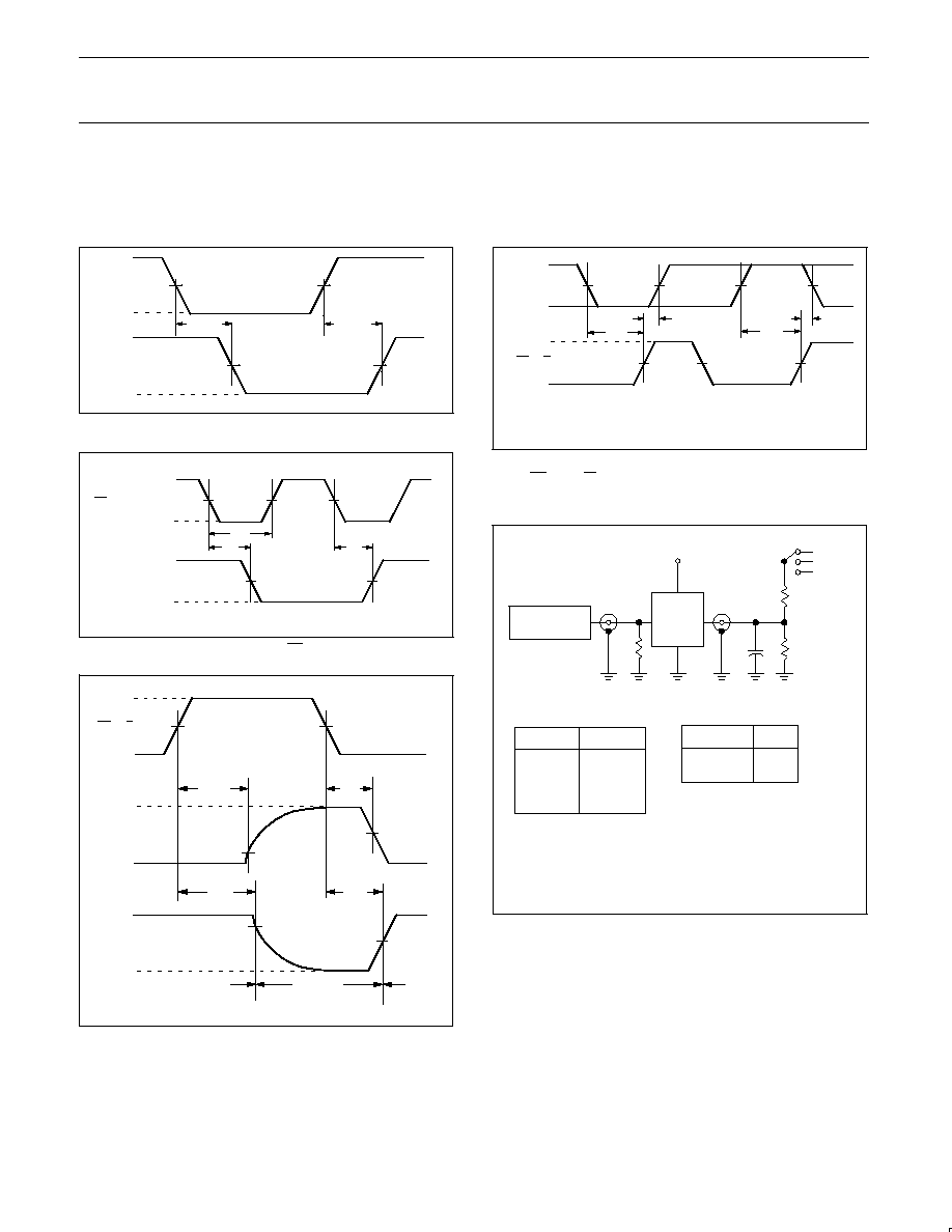
AC WAVEFORMS
V
M
= 1.5V at V
CC
w
2.7V; V
M
= 0.5 V
CC
at V
CC
t
2.7V.
V
OL
and V
OH
are the typical output voltage drop that occur with the output load.
V
X
= V
OL
+ 0.3V at V
CC
w
2.7V; V
X
= V
OL
+ 0.1 V
CC
at V
CC
t
2.7V
V
Y
= V
OH
≠0.3V at V
CC
w
2.7V; V
Y
= V
OH
≠ 0.1 V
CC
at V
CC
t
2.7V
SY00041
INPUT
V
M
tPHL
tPLH
V
OL
V
I
V
M
GND
V
OH
OUTPUT
Waveform 1. Input (A
n
, B
n
) to output (B
n
, A
n
) propagation
delays.
t
w
t
PHL
t
PLH
LE
XX
INPUT
A
n
, B
n
OUTPUT
V
M
V
M
V
M
V
M
V
M
V
I
GND
V
OH
V
OL
SA00408
Waveform 2. Latch enable input (LE
XX
) pulse width and the
latch enable input to output (A
n
, B
n
) propagation delays.
t
PLZ
t
PZL
V
I
OE
XX
, E
XX
INPUT
GND
V
CC
OUTPUT
LOW-to-OFF
OFF-to-LOW
V
OL
V
OH
OUTPUT
HIGH-to-OFF
OFF-to-HIGH
GND
outputs
enabled
outputs
enabled
outputs
disabled
t
PHZ
V
M
V
M
V
M
t
PZH
V
X
V
Y
SW00210
Waveform 3. 3-State enable and disable times
………
………
…………………
…………………
………
………
V
M
A
n
, B
n
INPUT
V
M
LE
XX
, E
XX
INPUT
t
SU
th
NOTE: The shaded areas indicate when the input is permitted to change
for predictable output performance.
t
SU
th
V
I
GND
V
I
GND
SW00211
Waveform 4. Data setup and hold times for the (A
n
, B
n
) input
to the LE
XX
and E
XX
inputs.
TEST CIRCUIT
PULSE
GENERATOR
RT
VIN
D.U.T.
VOUT
CL
VCC
R
L
=500
SWITCH POSITION
TEST
SWITCH
t
PLH
/t
PHL
Open
t
PLZ
/t
PZL
2
<
V
CC
t
PHZ
/t
PZH
GND
Test Circuit for 3-State Outputs
Open
GND
S
1
2
<
V
CC
DEFINITIONS
V
CC
t
2.7V
2.7 ≠ 3.6V
V
IN
V
CC
2.7V
R
L
= Load resistor
C
L
= Load capacitance includes jig and probe capacitance
R
T
= Termination resistance should be equal to Z
OUT
of pulse generators.
SW00047
R
L
=500
Waveform 5. Load circuitry for switching times.

Philips Semiconductors
Product specification
74LVC543A
Octal D-type registered transceiver (3-State)
1998 Jul 31
8
SO16:
plastic small outline package; 16 leads; body width 3.9 mm
SOT109-1

Philips Semiconductors
Product specification
74LVC543A
Octal D-type registered transceiver (3-State)
1998 Jul 31
9
SSOP16:
plastic shrink small outline package; 16 leads; body width 5.3 mm
SOT338-1
Philips Semiconductors
Product specification
74LVC543A
Octal D-type registered transceiver (3-State)
1998 Jul 31
10
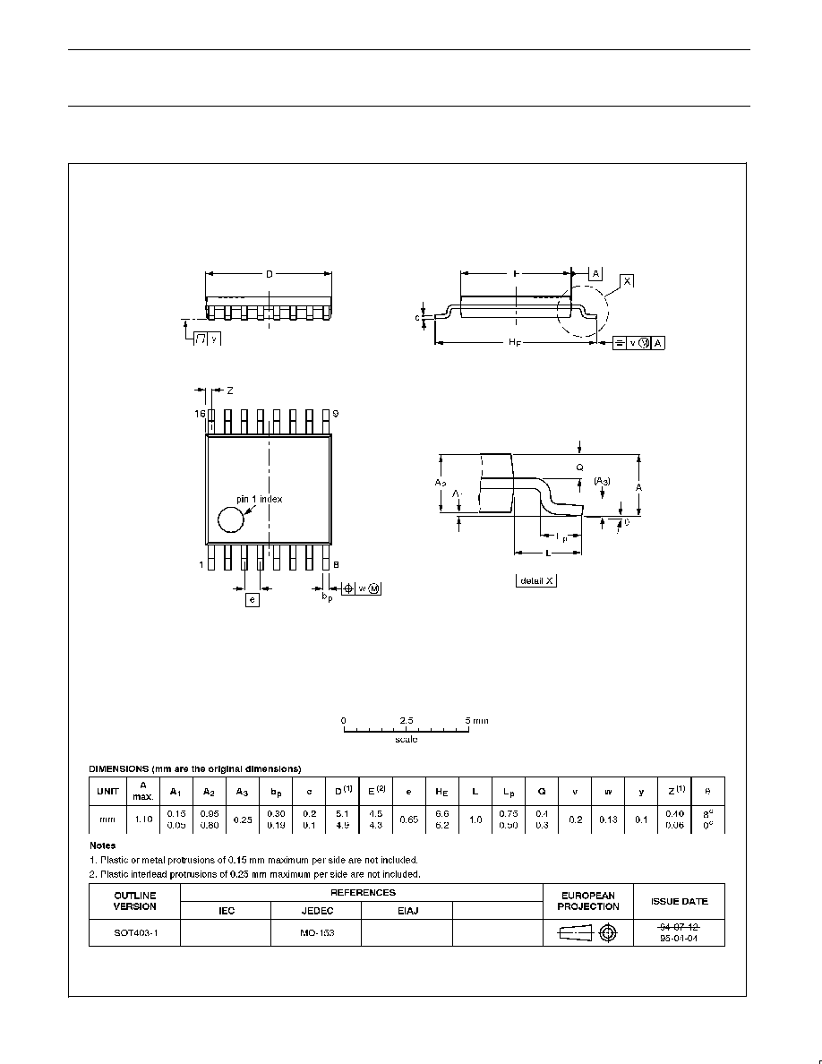
TSSOP16:
plastic thin shrink small outline package; 16 leads; body width 4.4 mm
SOT403-1

Philips Semiconductors
Product specification
74LVC543A
Octal D-type registered transceiver (3-State)
1998 Jul 31
11
NOTES

Philips Semiconductors
Product specification
74LVC543A
Octal D-type registered transceiver (3-State)
Philips
Semiconductors
Philips Semiconductors and Philips Electronics North America Corporation reserve the right to make changes, without notice, in the products,
including circuits, standard cells, and/or software, described or contained herein in order to improve design and/or performance. Philips
Semiconductors assumes no responsibility or liability for the use of any of these products, conveys no license or title under any patent, copyright,
or mask work right to these products, and makes no representations or warranties that these products are free from patent, copyright, or mask
work right infringement, unless otherwise specified. Applications that are described herein for any of these products are for illustrative purposes
only. Philips Semiconductors makes no representation or warranty that such applications will be suitable for the specified use without further testing
or modification.
LIFE SUPPORT APPLICATIONS
Philips Semiconductors and Philips Electronics North America Corporation Products are not designed for use in life support appliances, devices,
or systems where malfunction of a Philips Semiconductors and Philips Electronics North America Corporation Product can reasonably be expected
to result in a personal injury. Philips Semiconductors and Philips Electronics North America Corporation customers using or selling Philips
Semiconductors and Philips Electronics North America Corporation Products for use in such applications do so at their own risk and agree to fully
indemnify Philips Semiconductors and Philips Electronics North America Corporation for any damages resulting from such improper use or sale.
This data sheet contains preliminary data, and supplementary data will be published at a later date. Philips
Semiconductors reserves the right to make changes at any time without notice in order to improve design
and supply the best possible product.
Philips Semiconductors
811 East Arques Avenue
P.O. Box 3409
Sunnyvale, California 94088≠3409
Telephone 800-234-7381
DEFINITIONS
Data Sheet Identification
Product Status
Definition
Objective Specification
Preliminary Specification
Product Specification
Formative or in Design
Preproduction Product
Full Production
This data sheet contains the design target or goal specifications for product development. Specifications
may change in any manner without notice.
This data sheet contains Final Specifications. Philips Semiconductors reserves the right to make changes
at any time without notice, in order to improve design and supply the best possible product.
Philips Semiconductors and Philips Electronics North America Corporation
register eligible circuits under the Semiconductor Chip Protection Act.
©
Copyright Philips Electronics North America Corporation 1998
All rights reserved. Printed in U.S.A.
print code
Date of release: 05-96
Document order number:
9397-750-04511