
Philips
Semiconductors
74LVC823A
9-bit D-type flip-flop with 5-volt tolerant
inputs/outputs; positive-edge trigger
(3-State)
Product specification
1998 Sep 24
INTEGRATED CIRCUITS
Philips Semiconductors
Product specification
74LVC823A
9-bit D-type flip-flop with 5-volt tolerant
inputs/outputs; positive-edge trigger (3-State)
2
1998 Sep 24
853-2124 20078
FEATURES
∑
5-volt tolerant inputs/outputs, for interfacing with 5-volt logic
∑
Supply voltage range of 2.7V to 3.6V
∑
Complies with JEDEC standard no. 8-1A
∑
Inputs accept voltages up to 5.5V
∑
CMOS low power consumption
∑
Direct interface with TTL levels
∑
9-bit positive edge-triggered register
∑
Independent register and 3-State buffer operation
∑
Flow-through pin-out architecture
DESCRIPTION
The 74LVC823A is a high performance, low-power, low-voltage
Si-gate CMOS device and superior to most advanced CMOS
compatible TTL families.
Inputs can be driven from either 3.3V or 5.0V devices. In 3-state
operation, outputs can handle 5V. This feature allows the use of
these devices as translators in a mixed 3.3V/5V environment.
The 74LVC823A is a 9-bit D-type flip-flop with common clock (CP),
Clock Enable (CE), Master Reset (MR) and 3-State outputs for
bus-oriented applications.
The nine flip-flops will store the state of their individual D-inputs that
meet the set-up and hold times requirements on the LOW-to-HIGH
CP transition provided CE is LOW. When CE is HIGH the flip-flops
hold their data.
A LOW on MR resets all flip-flops.
When OE is LOW, the contents of the nine flip-flops is available at
the outputs. When OE is HIGH, the outputs go to the high
impedance OFF-state. Operation of the OE input does not affect the
state of the flip-flops.
QUICK REFERENCE DATA
GND = 0 V; T
amb
= 25
∞
C; t
r
= t
f
2.5 ns
SYMBOL
PARAMETER
CONDITIONS
TYPICAL
UNIT
t
/t
Propagation delay
CP to Q
n
C
L
= 50 pF;
5.1
ns
t
PHL
/t
PLH
Propagation delay
MR to Q
n
L
V
CC
= 3.3 V
5.2
ns
f
max
Maximum clock frequency
C
L
= 50 pF;
V
CC
= 3.3 V
150
MHz
C
I
Input capacitance
5.0
pF
C
PD
Power dissipation capacitance per
flip-flop
Notes 1 and 2
27
pF
NOTES:
1. C
PD
is used to determine the dynamic power dissipation (P
D
in
µ
W)
P
D
= C
PD
◊
V
CC
2
◊
f
i
)
(C
L
◊
V
CC
2
◊
f
o
) where:
f
i
= input frequency in MHz; C
L
= output load capacity in pF;
f
o
= output frequency in MHz; V
CC
= supply voltage in V;
(C
L
◊
V
CC
2
◊
f
o
) = sum of the outputs.
2. The condition is V
I
= GND to V
CC
ORDERING INFORMATION
PACKAGES
TEMPERATURE RANGE
ORDERING CODE
PKG. DWG. #
24-Pin Plastic SO
≠40
∞
C to +85
∞
C
74LVC823A D
SOT137-1
24-Pin Plastic SSOP Type II
≠40
∞
C to +85
∞
C
74LVC823A DB
SOT340-1
24-Pin Plastic TSSOP Type I
≠40
∞
C to +85
∞
C
74LVC823A PW
SOT355-1
Philips Semiconductors
Product specification
74LVC823A
9-bit D-type flip-flop with 5-volt tolerant
inputs/outputs; positive-edge trigger (3-State)
1998 Sep 24
3
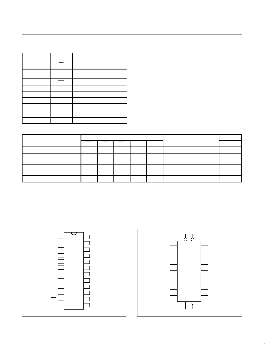
PIN DESCRIPTION
PIN NUMBER
SYMBOL
NAME AND FUNCTION
1
OE
Output enable input
(active LOW)
2, 3, 4, 5, 6,
7, 8, 9, 10
D
0
to D
8
Data inputs
11
MR
Master reset (active LOW)
12
GND
Ground (0 V)
13
CP
Clock pulse (active rising)
14
CE
Clock enable (active LOW)
23, 22, 21, 20,
19, 18, 17, 16,
15
Q
0
to Q
8
3-State flip-flop outputs
24
V
CC
Positive supply voltage
FUNCTION TABLE
OPERATING MODES
INPUTS
INTERNAL FLIP FLOPS
OUTPUTS
OPERATING MODES
OE
MR
CE
CP
D
n
INTERNAL FLIP-FLOPS
Q
0
to Q
8
Clear
L
L
X
X
X
L
L
Load and read register
L
L
H
H
L
L
l
h
L
H
L
H
Load register and disable outputs
H
H
H
H
L
L
X
X
l
h
L
H
Z
Z
Hold
L
H
H
NC
X
NC
NC
H = HIGH voltage level
h
= HIGH voltage level one set-up time prior to the LOW-to-HIGH
CP transition
L
= LOW voltage level
l
= LOW voltage level one set-up time prior to the LOW-to-HIGH
CP transition
Z = high impedance OFF-state
= LOW≠to≠HIGH clock transition
NC= no change
PIN CONFIGURATION
D 0
D 1
D 2
D 3
D 4
D 5
D 6
GND
D 7
D 8
MR
Q 0
Q 1
Q 2
Q 3
Q 4
V CC
Q 5
Q 6
Q 7
Q 8
CE
CP
1
2
3
4
5
6
7
8
9
10
11
12
20
21
22
23
24
19
18
17
16
15
14
13
OE
SA00418
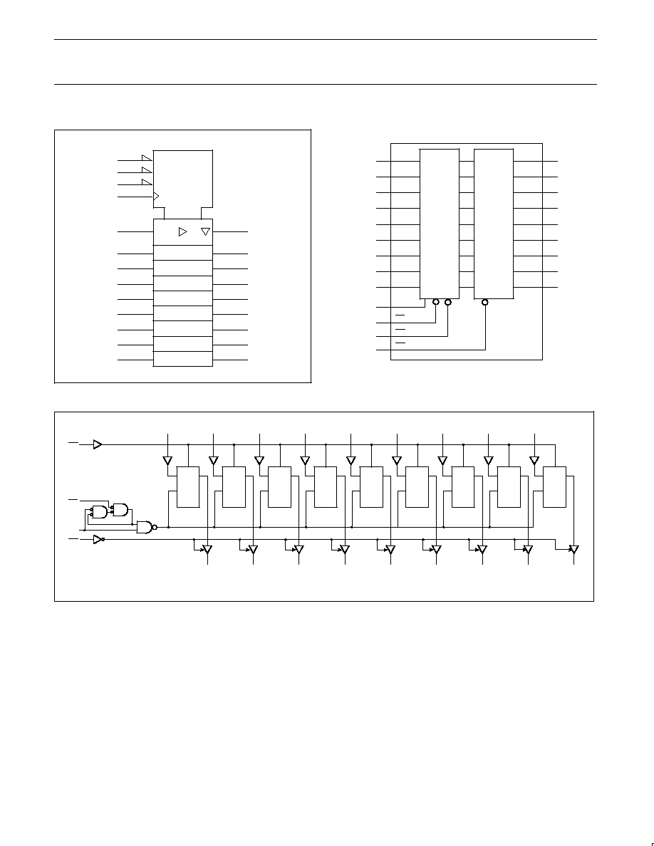
LOGIC SYMBOL
MR
11
Q 7
Q 8
2
D 0
Q 0
19
20
21
22
23
9
10
D 7
D 8
8
D 6
Q 6
7
D 5
Q 5
6
D 4
Q 4
15
5
D 3
Q 3
16
4
D 2
Q 2
17
3
D 1
Q 1
18
13
14
1
CP
CE
OE
SA00419
Philips Semiconductors
Product specification
74LVC823A
9-bit D-type flip-flop with 5-volt tolerant
inputs/outputs; positive-edge trigger (3-State)
1998 Sep 24
4
LOGIC SYMBOL (IEEE/IEC)
23
22
21
20
19
18
17
16
15
2
3
4
5
6
7
8
9
10
G1
EN
1C2
R
13
14
11
1
2D
SA00420
FUNCTIONAL DIAGRAM
FF0 to FF8
3≠STATE
OUTPUTS
Q0
Q1
Q2
Q3
Q4
Q5
Q6
Q7
Q8
D0
D1
D2
D3
D4
D5
D6
D7
D8
CP
11
14
1
19
20
21
22
23
18
17
16
15
OE
MR
CE
2
3
4
5
6
7
8
9
10
13
SA00421
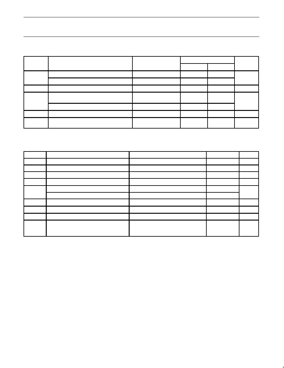
LOGIC DIAGRAM
D0
D1
D2
D3
D4
D5
D6
D7
D8
CP
OE
CE
MR
D
R
R
R
R
R
R
R
R
R
CP
CP
CP
CP
CP
CP
CP
CP
CP
Q
FF1
D
Q
FF2
D
Q
FF3
D
Q
FF4
D
Q
FF5
D
Q
FF6
D
Q
FF7
D
D
Q
Q
FF8
FF0
Q0
Q1
Q2
Q3
Q4
Q5
Q6
Q7
Q8
SA00422
Philips Semiconductors
Product specification
74LVC823A
9-bit D-type flip-flop with 5-volt tolerant
inputs/outputs; positive-edge trigger (3-State)
1998 Sep 24
5
RECOMMENDED OPERATING CONDITIONS
SYMBOL
PARAMETER
CONDITIONS
LIMITS
UNIT
SYMBOL
PARAMETER
CONDITIONS
MIN
MAX
UNIT
V
CC
DC supply voltage (for max. speed performance)
2.7
3.6
V
V
CC
DC supply voltage (for low-voltage applications)
1.2
3.6
V
V
I
DC Input voltage range
0
5.5
V
V
O
DC output voltage range; output HIGH or LOW
state
0
V
CC
V
O
DC output voltage range; output 3-State
0
5.5
T
amb
Operating ambient temperature range in free-air
≠40
+85
∞
C
t
r
, t
f
Input rise and fall times
V
CC
= 1.2 to 2.7V
V
CC
= 2.7 to 3.6V
0
0
20
10
ns/V
ABSOLUTE MAXIMUM RATINGS
1
In accordance with the Absolute Maximum Rating System (IEC 134)
Voltages are referenced to GND (ground = 0V)
SYMBOL
PARAMETER
CONDITIONS
RATING
UNIT
V
CC
DC supply voltage
≠0.5 to +6.5
V
I
IK
DC input diode current
V
I
t
0
≠50
mA
V
I
DC input voltage
Note 2
≠0.5 to +6.5
V
I
OK
DC output diode current
V
O
u
V
CC
or V
O
t
0
"
50
mA
V
O
DC output voltage; output HIGH or LOW state
Note 2
≠0.5 to V
CC
+0.5
V
V
O
DC output voltage; output 3-State
Note 2
≠0.5 to 6.5
V
I
O
DC output source or sink current
V
O
= 0 to V
CC
"
50
mA
I
GND
, I
CC
DC V
CC
or GND current
"
100
mA
T
stg
Storage temperature range
≠65 to +150
∞
C
Power dissipation per package
P
TOT
≠ plastic mini-pack (SO)
above +70
∞
C derate linearly with 8 mW/K
500
mW
≠ plastic shrink mini-pack (SSOP and TSSOP)
above +60
∞
C derate linearly with 5.5 mW/K
500
mW
NOTES:
1. Stresses beyond those listed may cause permanent damage to the device. These are stress ratings only and functional operation of the
device at these or any other conditions beyond those indicated under "recommended operating conditions" is not implied. Exposure to
absolute-maximum-rated conditions for extended periods may affect device reliability.
2. The input and output voltage ratings may be exceeded if the input and output current ratings are observed.