74LVT16240A 3.3 V LVT 16-bit inverting buffer/driver (3-State)
Philips
Semiconductors
74LVT16240A
3.3 V LVT 16-bit inverting buffer/driver
(3-State)
Product data
Supersedes data of 1998 Feb 19
2003 Feb 21
INTEGRATED CIRCUITS
Philips Semiconductors
Product data
74LVT16240A
3.3 V 16-bit inverting buffer/driver (3-State)
2
2003 Feb 21
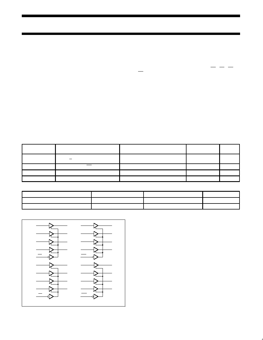
FEATURES
·
16-bit bus interface
·
3-State buffers
·
Output capability: +64 mA/32 mA
·
TTL input and output switching levels
·
Input and output interface capability to systems at 5 V supply
·
Bus-hold data inputs eliminate the need for external pull-up
resistors to hold unused inputs
·
Live insertion/extraction permitted
·
Power-up 3-State
·
No bus current loading when output is tied to 5 V bus
·
Latch-up protection exceeds 500 mA per JEDEC Std 17
·
ESD protection exceeds 2000 V per MIL STD 883 Method 3015
and 200 V per Machine Model
DESCRIPTION
The 74LVT16240A is a high-performance BiCMOS product
designed for V
CC
operation at 3.3 V.
This device is an inverting 16-bit buffer that is ideal for driving bus
lines. The device features four Output Enables (1OE, 2OE, 3OE,
4OE), each controlling four of the 3-State outputs.
QUICK REFERENCE DATA
SYMBOL
PARAMETER
CONDITIONS
T
amb
= 25
°
C
TYPICAL
UNIT
t
PLH
t
PHL
Propagation delay
nAx to nYx
C
L
= 50 pF;
V
CC
= 3.3 V
1.9
ns
C
IN
Input capacitance nOE
V
I
= 0 V or 3.0 V
3
pF
C
OUT
Output capacitance
Outputs disabled; V
O
= 0 V or 3.0 V
9
pF
I
CCZ
Total supply current
Outputs disabled; V
CC
= 3.6 V
70
µ
A
ORDERING INFORMATION
PACKAGES
TEMPERATURE RANGE
PART NUMBER
DWG NUMBER
48-Pin Plastic SSOP Type III
40
°
C to +85
°
C
74LVT16240ADL
SOT370-1
48-Pin Plastic TSSOP Type II
40
°
C to +85
°
C
74LVT16240ADGG
SOT362-1
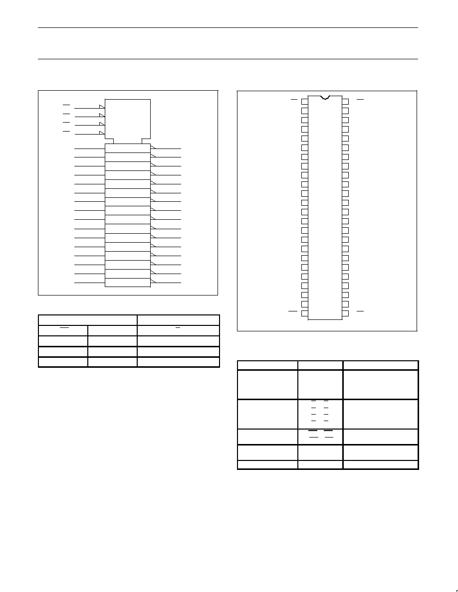
LOGIC SYMBOL
1OE
1
1A0
47
1A1
46
1A2
44
1A3
43
2OE
48
2A0
41
2A1
2
40
2A2
38
3
2A3
37
5
6
1Y0
1Y1
1Y2
1Y3
2Y0
2Y1
2Y2
2Y3
8
9
11
12
3OE
25
3A0
36
3A1
35
3A2
33
3A3
32
4OE
24
4A0
30
4A1
13
29
4A2
27
14
4A3
26
16
17
3Y0
3Y1
3Y2
3Y3
4Y0
4Y1
4Y2
4Y3
19
20
22
23
SA00014
Philips Semiconductors
Product data
74LVT16240A
3.3 V 16-bit inverting buffer/driver (3-State)
2003 Feb 21
3
LOGIC SYMBOL (IEEE/IEC)
48
EN1
1
46
44
43
41
40
38
37
36
EN2
EN3
EN4
1
2
1
3
1
4
1
1
25
24
47
35
33
32
30
29
27
26
3
2
5
6
8
9
11
12
13
14
16
17
19
20
22
23
SW00059
1OE
2OE
3OE
4OE
1A0
1A1
1A2
1A3
2A0
2A1
2A2
3A0
3A1
3A2
3A3
4A0
4A1
4A2
4A3
1Y0
1Y1
1Y2
1Y3
2Y0
2Y1
2Y2
2Y3
3Y0
3Y1
3Y2
3Y3
4Y0
4Y3
2A3
4Y1
4Y2
FUNCTION TABLE
Inputs
Outputs
nOE
nAx
nYx
L
L
H
L
H
L
H
X
Z
H = HIGH voltage level
L = LOW voltage level
X = Don't care
Z = High Impedance "off " state
PIN CONFIGURATION
1
2
3
4
5
6
7
8
9
10
11
12
13
14
15
16
17
18
19
20
21
22
23
24
48
47
46
45
44
43
42
41
40
39
38
37
36
35
34
33
32
31
30
29
28
27
26
25
1OE
1Y0
1Y1
GND
1Y2
1Y3
2Y0
2Y1
GND
2Y2
2Y3
3Y0
3Y1
GND
3Y4
VCC
4Y0
VCC
3Y2
4Y1
GND
4Y3
4OE
4Y2
2OE
1A0
1A1
GND
1A2
1A3
2A0
2A1
GND
2A2
2A3
3A0
3A1
GND
3A3
V
CC
4A0
VCC
3A2
4A1
GND
4A3
3OE
4A2
SA00013
PIN DESCRIPTION
PIN NUMBER
SYMBOL
NAME AND FUNCTION
47, 46, 44, 43,
41, 40, 38, 37,
36, 35, 33, 32,
30, 29, 27, 26
1A0-1A3
2A0-2A3
3A0-3A3
4A0-4A3
Data inputs
2, 3, 5, 6,
8, 9, 11, 12,
13, 14, 16, 17,
19, 20, 22, 23
1Y0-1Y3
2Y0-2Y3
3Y0-3Y3
4Y0-4Y3
Data outputs
1, 48, 25, 24
1OE, 2OE,
3OE, 4OE
Output Enables
4, 10, 15, 21,
28, 34, 39, 45
GND
Ground (0 V)
7, 18, 31, 42
V
CC
Positive supply voltage
Philips Semiconductors
Product data
74LVT16240A
3.3 V 16-bit inverting buffer/driver (3-State)
2003 Feb 21
4
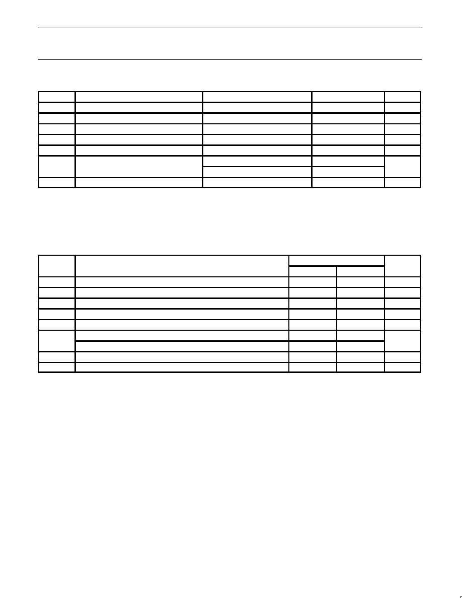
ABSOLUTE MAXIMUM RATINGS
1, 2
SYMBOL
PARAMETER
CONDITIONS
RATING
UNIT
V
CC
DC supply voltage
0.5 to +4.6
V
I
IK
DC input diode current
V
I
< 0 V
50
mA
V
I
DC input voltage
3
0.5 to +7.0
V
I
OK
DC output diode current
V
O
< 0 V
50
mA
V
OUT
DC output voltage
3
Output in Off or HIGH state
0.5 to +7.0
V
I
O
DC output current
Output in LOW state
128
mA
I
OUT
DC output current
Output in HIGH state
64
mA
T
stg
Storage temperature range
65 to +150
°
C
NOTES:
1. Stresses beyond those listed may cause permanent damage to the device. These are stress ratings only and functional operation of the
device at these or any other conditions beyond those indicated under "recommended operating conditions" is not implied. Exposure to
absolute-maximum-rated conditions for extended periods may affect device reliability.
2. The performance capability of a high-performance integrated circuit in conjunction with its thermal environment can create junction
temperatures which are detrimental to reliability. The maximum junction temperature of this integrated circuit should not exceed 150
°
C.
3. The input and output negative voltage ratings may be exceeded if the input and output clamp current ratings are observed.
RECOMMENDED OPERATING CONDITIONS
SYMBOL
PARAMETER
LIMITS
UNIT
SYMBOL
PARAMETER
MIN
MAX
UNIT
V
CC
DC supply voltage
2.7
3.6
V
V
I
Input voltage
0
5.5
V
V
IH
HIGH-level input voltage
2.0
V
V
IL
Input voltage
0.8
V
I
OH
HIGH-level output current
32
mA
I
OL
LOW-level output current
32
mA
LOW-level output current; current duty cycle
50%; f
1 kHz
64
t/
v
Input transition rise or fall rate; Outputs enabled
10
ns/V
T
amb
Operating free-air temperature range
-40
+85
°
C
Philips Semiconductors
Product data
74LVT16240A
3.3 V 16-bit inverting buffer/driver (3-State)
2003 Feb 21
5
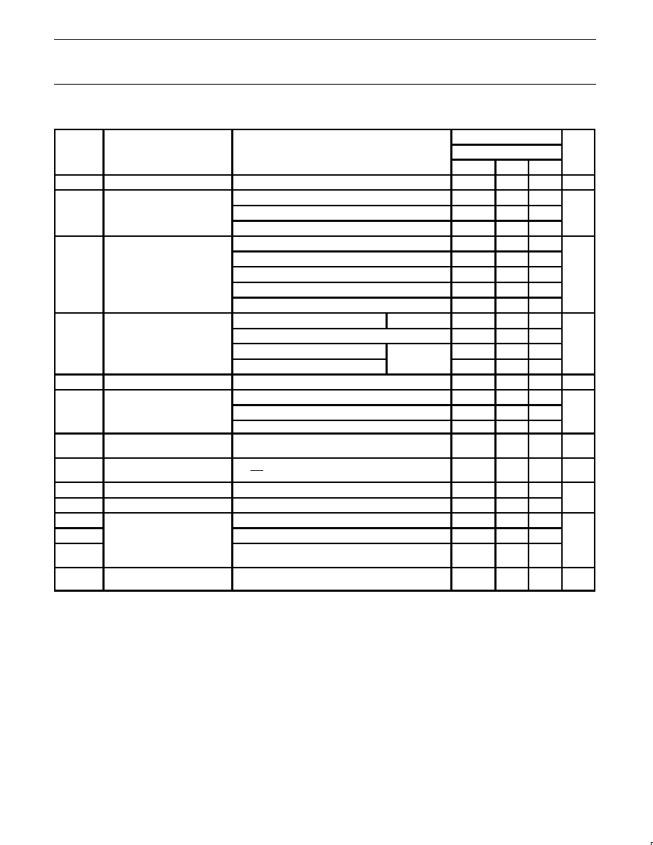
DC ELECTRICAL CHARACTERISTICS
LIMITS
SYMBOL
PARAMETER
TEST CONDITIONS
T
amb
= 40
°
C to +85
°
C
UNIT
MIN
TYP
1
MAX
V
IK
Input clamp voltage
V
CC
= 2.7 V; I
IK
= 18 mA
0.85
1.2
V
V
CC
= 2.7 V to 3.6 V; I
OH
= 100
µ
A
V
CC
0.2
V
CC
V
OH
HIGH-level output voltage
V
CC
= 2.7 V; I
OH
= 8 mA
2.4
2.5
V
V
CC
= 3.0 V; I
OH
= 32 mA
2.0
2.3
V
CC
= 2.7 V; I
OL
= 100
µ
A
0.07
0.2
V
CC
= 2.7 V; I
OL
= 24 mA
0.03
0.5
V
OL
LOW-level output voltage
V
CC
= 3.0 V; I
OL
= 16 mA
0.25
0.4
V
V
CC
= 3.0 V; I
OL
= 32 mA
0.30
0.5
V
CC
= 3.0 V; I
OL
= 64 mA
0.40
0.55
V
CC
= 3.6 V; V
I
= V
CC
or GND
Control pins
0.1
±
1.0
I
Input leakage current
V
CC
= 0 V or 3.6 V; V
I
= 5.5 V
0.4
10
µ
A
I
I
Input leakage current
V
CC
= 3.6 V; V
I
= V
CC
Data pins
4
0.1
1
µ
A
V
CC
= 3.6 V; V
I
= 0 V
Data pins
4
0.4
5
I
OFF
Output off current
V
CC
= 0 V; V
I
or V
O
= 0 V to 4.5 V
0.1
±
100
µ
A
6
V
CC
= 3 V; V
I
= 0.8 V
75
135
I
HOLD
Bus Hold current A inputs
6
V
CC
= 3 V; V
I
= 2.0 V
75
135
µ
A
V
CC
= 0 V to 3.6 V; V
CC
= 3.6 V
±
500
I
EX
Current into an output in the
HIGH state when V
O
> V
CC
V
O
= 5.5 V; V
CC
= 3.0 V
50
125
µ
A
I
PU/PD
Power-up/-down 3-State output
current
3
V
CC
1.2 V; V
O
= 0.5 V to V
CC
; V
I
= GND or V
CC
OE/OE = Don't care
1
±
100
µ
A
I
OZH
3-State output HIGH current
V
CC
= 3.6 V; V
O
= 3.0 V; V
I
= V
IL
or V
IH
0.5
5
µ
A
I
OZL
3-State output LOW current
V
CC
= 3.6 V; V
O
= 0.5 V; V
I
= V
IL
or V
IH
0.5
5
µ
A
I
CCH
V
CC
= 3.6 V; Outputs High, V
I
= GND or V
CC,
I
O =
0
0.07
0.12
I
CCL
Quiescent supply current
V
CC
= 3.6 V; Outputs Low, V
I
= GND or V
CC,
I
O =
0
4.0
6.0
mA
I
CCZ
V
CC
= 3.6 V; Outputs Disabled;
V
I
= GND or V
CC,
I
O
= 0
5
0.07
0.12
I
CC
Additional supply current per
input pin
2
V
CC
= 3V to 3.6V; One input at V
CC
0.6V,
Other inputs at V
CC
or GND
0.1
0.20
mA
NOTES:
1. All typical values are at V
CC
= 3.3 V and T
amb
= 25
°
C.
2. This is the increase in supply current for each input at the specified voltage level other than V
CC
or GND.
3. This parameter is valid for any V
CC
between 0 V and 1.2 V with a transition time of up to 10 msec. From V
CC
= 1.2 V to V
CC
= 3.3 V
±
0.3 V
a transition time of 100
µ
sec is permitted. This parameter is valid for T
amb
= 25
°
C only.
4. Unused pins at V
CC
or GND.
5. I
CCZ
is measured with outputs pulled to V
CC
or GND.
6. This is the bus hold overdrive current required to force the input to the opposite logic state.
Document Outline
- FEATURES
- DESCRIPTION
- QUICK REFERENCE DATA
- ORDERING INFORMATION
- LOGIC SYMBOL
- LOGIC SYMBOL (IEEE/IEC)
- FUNCTION TABLE
- PIN CONFIGURATION
- PIN DESCRIPTION
- ABSOLUTE MAXIMUM RATINGS 1, 2
- RECOMMENDED OPERATING CONDITIONS
- DC ELECTRICAL CHARACTERISTICS
- AC CHARACTERISTICS
- AC WAVEFORMS
- TEST CIRCUIT AND WAVEFORMS
- PACKAGE OUTLINE
- REVISION HISTORY
- Data sheet status
- Definitions
- Disclaimers