Philips Semiconductors
Product specification
74LVT646
3.3V Octal bus transceiver/register (3-State)
2
1998 Feb 19
853-1747 18987
FEATURES
·
Combines 74LVT245 and 74LVT574 type functions in one device
·
Independent registers for A and B buses
·
Multiplexed realtime and stored data
·
Output capability: +64mA/32mA
·
TTL input and output switching levels
·
Input and output interface capability to systems at 5V supply
·
Bus-hold data inputs eliminate the need for external pull-up
resistors to hold unused inputs
·
Live insertion/extraction permitted
·
No bus current loading when output is tied to 5V bus
·
Latch-up protection exceeds 500mA per JEDEC Std 17
·
Power-up 3-State
·
Power-up reset
·
ESD protection exceeds 2000V per MIL STD 883 Method 3015
and 200V per Machine Model
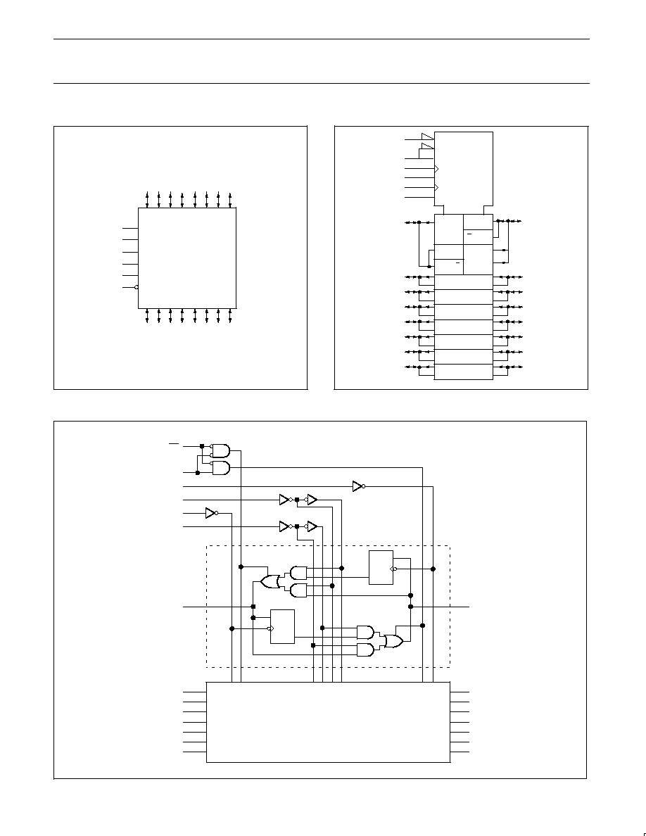
DESCRIPTION
The LVT646 is a high-performance BiCMOS product designed for
V
CC
operation at 3.3V.
This device consists of bus transceiver circuits with 3-State outputs,
D-type flip-flops, and control circuitry arranged for multiplexed
transmission of data directly from the input bus or the internal
registers.
Data on the A or B bus will be clocked into the registers as the
appropriate clock pin goes High.
Output Enable (OE) and DIR pins are provided to control the
transceiver function. In the transceiver mode, data present at the
high impedance port may be stored in either the A or B register or
both.
The Select (SAB, SBA) pins determine whether data is stored or
transferred through the device in realtime. The DIR determines
which bus will receive data when the OE is active (Low).
In the isolation mode (OE = High), data from Bus A may be stored in
the B register and/or data from Bus B may be stored in the A
register.
When an output function is disabled, the input function is still
enabled and may be used to store and transmit data. Only one of
the two buses, A or B may be driven at a time. The examples on the
next page demonstrate the four fundamental bus management
functions that can be performed with the 74LVT646.
QUICK REFERENCE DATA
SYMBOL
PARAMETER
CONDITIONS
T
amb
= 25
°
C; GND = 0V
TYPICAL
UNIT
t
PLH
t
PHL
Propagation delay
An to Bn or Bn to An
C
L
= 50pF; V
CC
= 3.3V
2.8
2.7
ns
C
IN
Input capacitance
CP, S, OE, DIR
V
I/O
= 0V or 3.0V
4
pF
C
I/O
I/O capacitance
Outputs disabled; V
I/O
= 0V or 3.0V
10
pF
I
CCZ
Total supply current
Outputs disabled; V
CC
= 3.6V
0.13
mA
ORDERING INFORMATION
PACKAGES
TEMPERATURE RANGE
OUTSIDE NORTH AMERICA
NORTH AMERICA
DWG NUMBER
24-Pin Plastic SOL
40
°
C to +85
°
C
74LVT646 D
74LVT646 D
SOT163-1
24-Pin Plastic SSOP Type II
40
°
C to +85
°
C
74LVT646 DB
74LVT646 DB
SOT399-1
24-Pin Plastic TSSOP Type I
40
°
C to +85
°
C
74LVT646 PW
74LVT646PW DH
SOT360-1
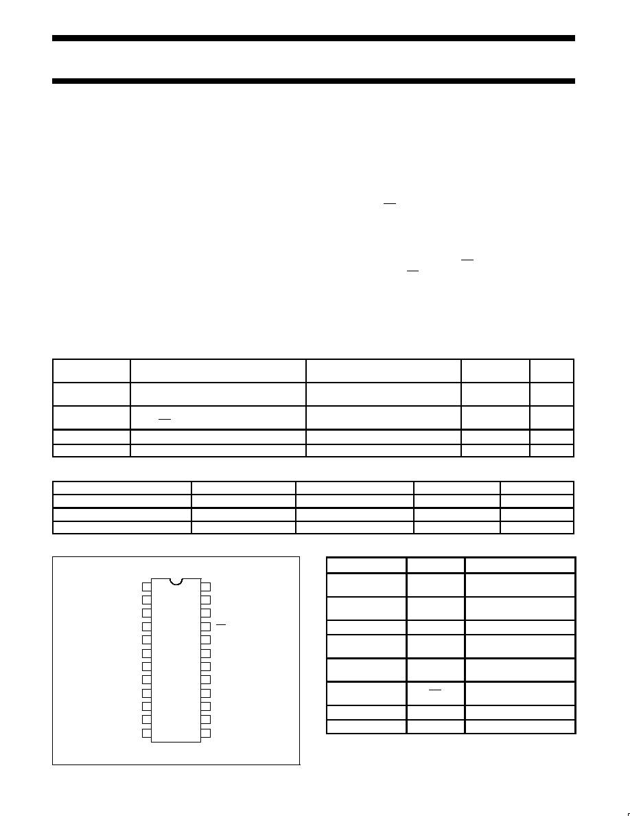
PIN CONFIGURATION
VCC
CPBA
SBA
OE
B0
B1
B2
B3
B4
B5
B6
B7
CPAB
SAB
DIR
A0
A1
A2
A3
A4
A5
A6
A7
GND
24
23
22
21
20
19
18
17
16
15
14
13
1
2
3
4
5
6
7
8
9
10
11
12
SV00045
PIN DESCRIPTION
PIN NUMBER
SYMBOL
FUNCTION
1, 23
CPAB /
CPBA
A to B clock input / B to A
clock input
2, 22
SAB / SBA
A to B select input / B to
A select input
3
DIR
Direction control input
4, 5, 6, 7, 8, 9, 10,
11
A0 A7
Data inputs/outputs (A
side)
20, 19, 18, 17, 16,
15, 14, 13
B0 B7
Data inputs/outputs (B
side)
21
OE
Output enable input
(active-low)
12
GND
Ground (0V)
24
V
CC
Positive supply voltage
Philips Semiconductors
Product specification
74LVT646
3.3V Octal bus transceiver/register (3-State)
1998 Feb 19
4
}
REAL TIME BUS TRANSFER
BUS B TO BUS A
OE
DIR CPAB CPBA SAB
SBA
L
L
X
X
X
L
}
REAL TIME BUS TRANSFER
BUS A TO BUS B
OE
DIR CPAB CPBA SAB
SBA
L
H
X
X
L
X
}
STORAGE FROM
A, B, OR A AND B
OE
DIR CPAB CPBA SAB
SBA
L
H
X
X
X
L
L
X
X
X
H
X
X
X
}
TRANSFER STORED DATA
TO A OR B
OE
DIR CPAB CPBA SAB
SBA
L
L
X
H or L
X
H
L
H
H or L
X
H
X
A
A
A
A
B
B
B
B
SV00049
FUNCTION TABLE
INPUTS
DATA I/O
OPERATING MODE
OE
DIR
CPAB
CPBA
SAB
SBA
An
Bn
OPERATING MODE
X
X
X
X
X
Input
Unspecified
output*
Store A, B unspecified
X
X
X
X
X
Unspecified
output*
Input
Store B, A unspecified
H
H
X
X
H or L
H or L
X
X
X
X
Input
Input
Store A and B data
Isolation, hold storage
L
L
L
L
X
X
X
H or L
X
X
L
H
Output
Input
Real time B data to A bus
Stored B data to A bus
L
L
H
H
X
H or L
X
X
L
H
X
X
Input
Output
Real time A data to B bus
Stored A data to B bus
H = High voltage level
L
= Low voltage level
X = Don't care
= Low-to-High clock transition
*
The data output function may be enabled or disabled by various signals at the OE input. Data input functions are always enabled, i.e.,
data at the bus pins will be stored on every Low-to-High transition of the clock.
Philips Semiconductors
Product specification
74LVT646
3.3V Octal bus transceiver/register (3-State)
1998 Feb 19
5
ABSOLUTE MAXIMUM RATINGS
1, 2
SYMBOL
PARAMETER
CONDITIONS
RATING
UNIT
V
CC
DC supply voltage
0.5 to +4.6
V
I
IK
DC input diode current
V
I
< 0
50
mA
V
I
DC input voltage
3
0.5 to +7.0
V
I
OK
DC output diode current
V
O
< 0
50
mA
V
OUT
DC output voltage
3
Output in Off or High state
0.5 to +7.0
V
I
O
DC output current
Output in Low state
128
mA
I
OUT
DC output current
Output in High state
64
mA
T
stg
Storage temperature range
65 to 150
°
C
NOTES:
1. Stresses beyond those listed may cause permanent damage to the device. These are stress ratings only and functional operation of the
device at these or any other conditions beyond those indicated under "recommended operating conditions" is not implied. Exposure to
absolute-maximum-rated conditions for extended periods may affect device reliability.
2. The performance capability of a high-performance integrated circuit in conjunction with its thermal environment can create junction
temperatures which are detrimental to reliability. The maximum junction temperature of this integrated circuit should not exceed 150
°
C.
3. The input and output negative voltage ratings may be exceeded if the input and output clamp current ratings are observed.
RECOMMENDED OPERATING CONDITIONS
SYMBOL
PARAMETER
LIMITS
UNIT
SYMBOL
PARAMETER
MIN
MAX
UNIT
V
CC
DC supply voltage
2.7
3.6
V
V
I
Input voltage
0
5.5
V
V
IH
High-level input voltage
2.0
V
V
IL
Input voltage
0.8
V
I
OH
High-level output current
32
mA
I
O
Low-level output current
32
mA
I
OL
Low-level output current; current duty cycle
50%, f
1kHz
64
mA
t/
v
Input transition rise or fall rate; Outputs enabled
10
ns/V
T
amb
Operating free-air temperature range
40
+85
°
C