
Philips
Semiconductors
74LVC623A
Octal transceiver with dual enable
(3-State)
Product specification
1998 Jul 29
INTEGRATED CIRCUITS

Philips Semiconductors
Product specification
74LVC623A
Octal transceiver with dual enable (3-State)
2
1998 Jul 29
853-2106 19803
FEATURES
∑
Wide supply voltage range of 1.2V to 3.6V
∑
In accordance with JEDEC standard no. 8-1A
∑
Flow-through pin-out architecture
∑
CMOS low power consumption
∑
Inputs accept voltages up to 5.5V
∑
Direct interface with TTL levels
∑
Output drive capability 50
W
transmission lines @ 85
∞
C
DESCRIPTION
The 74LVC623A is a high performance, low-power, low-voltage
Si-gate CMOS device, superior to most advanced CMOS
compatible TTL families.
The 74LVC623A is an octal transceiver featuring non-inverting
3-State bus compatible outputs in both send and receive directions.
This octal bus transceiver is designed for asynchronous two-way
communication between data buses.
The control function implementation allows maximum flexibility in
timing. This device allows data transmission from the A bus to the B
bus or from the B bus to the A bus, depending upon the levels at the
enable inputs (OEAB, OEBA). The enable inputs can be used to
disable the device so that the buses are effectively isolated. The
dual enable function configuration gives this transceiver the
capability to store data by simultaneous enabling of OEAB and
OEBA. Each output reinforces its input in this transceiver
configuration. Thus, when both control inputs are enabled and all
other data sources to the two sets of the bus lines are at high
impedance OFF-state, both sets of bus lines will remain at their last
states. The 8-bit codes appearing on the two sets of buses will be
identical.
The `623A' is identical to the `620A' but has true (non-inverting)
outputs.
QUICK REFERENCE DATA
GND = 0V; T
amb
= 25
∞
C; t
r
= t
f
v
2.5 ns
SYMBOL
PARAMETER
CONDITIONS
TYPICAL
UNIT
t
PHL
/t
PLH
Propagation delay
An to Bn; Bn to An
C
L
= 50pF
V
CC
= 3.3V
3.3
ns
C
I
Input capacitance
5.0
pF
C
I/O
Input/output capacitance
10
pF
C
PD
Power dissipation capacitance per latch
Notes 1, 2
32
pF
NOTES:
1. C
PD
is used to determine the dynamic power dissipation (P
D
in
µ
W)
P
D
= C
PD
V
CC
2
x f
i
)
(C
L
V
CC
2
f
o
) where:
f
i
= input frequency in MHz; C
L
= output load capacity in pF;
f
o
= output frequency in MHz; V
CC
= supply voltage in V;
(C
L
V
CC
2
f
o
) = sum of the outputs.
2. The condition is V
I
= GND to V
CC.
ORDERING AND PACKAGE INFORMATION
PACKAGES
TEMPERATURE RANGE
OUTSIDE NORTH
AMERICA
NORTH AMERICA
PKG. DWG. #
20-Pin Plastic SO
≠40
∞
C to +85
∞
C
74LVC623A D
74LVC623A D
SOT163-1
20-Pin Plastic SSOP Type II
≠40
∞
C to +85
∞
C
74LVC623A DB
74LVC623A DB
SOT339-1
20-Pin Plastic TSSOP Type I
≠40
∞
C to +85
∞
C
74LVC623A PW
7LVC623APW DH
SOT360-1
Philips Semiconductors
Product specification
74LVC623A
Octal transceiver with dual enable (3-State)
1998 Jul 29
3
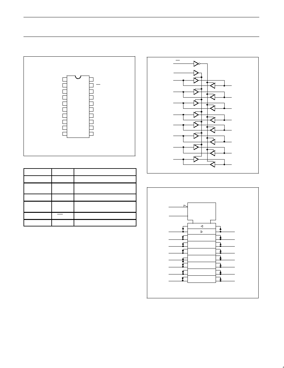
PIN CONFIGURATION
1
2
3
4
5
6
7
8
9
10
11
12
13
14
15
16
17
18
19
20
OEAB
A0
A1
A2
A3
A4
A5
A6
A7
GND
VCC
OEBA
B0
B1
B2
B3
B4
B5
B6
B7
SV00744
PIN DESCRIPTION
PIN NUMBER
SYMBOL
NAME AND FUNCTION
1
OEAB
Direction control
2, 3, 4, 5,
6, 7, 8, 9
A0 ≠ A7
Data inputs/outputs
10
GND
Ground (0V)
18, 17, 16, 15,
14, 13, 12, 11
B0 ≠ B7
Data inputs/outputs
19
OEBA
Output enable input (active LOW)
20
V
CC
Positive supply voltage
LOGIC SYMBOL
1
2
3
4
5
6
7
8
9
19
18
17
16
15
14
13
12
11
A0
A1
A2
A3
A4
A5
A6
A7
B0
B1
B2
B3
B4
B5
B6
B7
SV00745
OEAB
OEBA
LOGIC SYMBOL (IEEE/IEC)
19
EN1
1
EN2
1
2
2
3
4
5
6
7
8
9
18
17
16
15
14
13
12
11
SV00746
Philips Semiconductors
Product specification
74LVC623A
Octal transceiver with dual enable (3-State)
1998 Jul 29
4
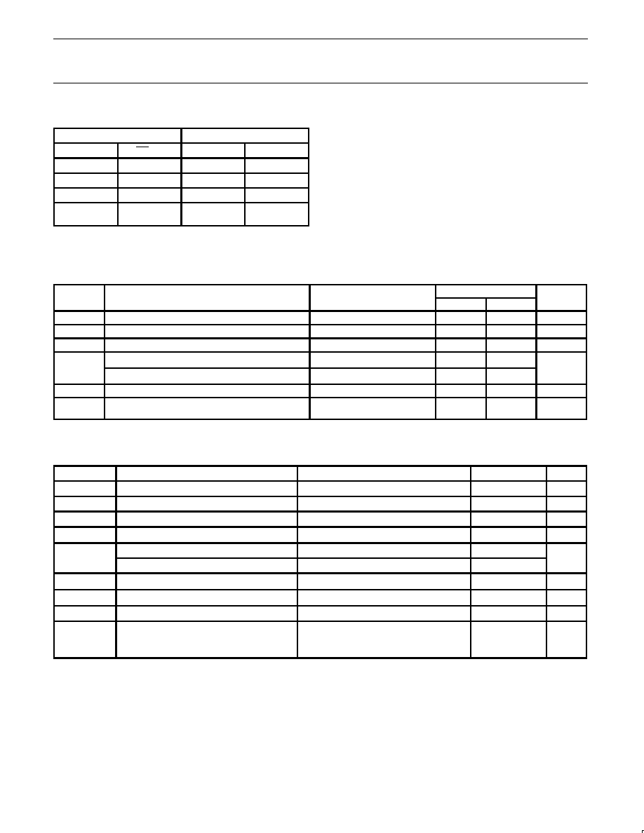
FUNCTION TABLE
INPUTS
INPUTS/OUTPUT
OEAB
OEBA
An
Bn
L
L
A=B
Inputs
H
H
Inputs
B=A
L
H
Z
Z
H
L
A=B
Inputs
Inputs
B=A
H = High voltage level
L
= Low voltage level
Z =High impedance
RECOMMENDED OPERATING CONDITIONS
SYMBOL
PARAMETER
CONDITIONS
LIMITS
UNIT
SYMBOL
PARAMETER
CONDITIONS
MIN
MAX
UNIT
V
CC
DC supply voltage (for max. speed performance)
2.7
3.6
V
V
CC
DC supply voltage (for low-voltage applications)
1.2
3.6
V
V
I
DC input voltage range
0
5.5
V
V
DC output voltage range; output HIGH or LOW state
0
V
CC
V
V
O
DC output voltage range; output 3-State
0
5.5
V
T
amb
Operating free-air temperature range
≠40
+85
∞
C
t
r
, t
f
Input rise and fall times
V
CC
= 1.2 to 2.7V
V
CC
= 2.7 to 3.6V
0
0
20
10
ns/V
ABSOLUTE MAXIMUM RATINGS
1
In accordance with the Absolute Maximum Rating System (IEC 134)
Voltages are referenced to GND (ground = 0V)
SYMBOL
PARAMETER
CONDITIONS
RATING
UNIT
V
CC
DC supply voltage
≠0.5 to +6.5
V
I
IK
DC input diode current
V
I
t
0
≠50
mA
V
I
DC input voltage
Note 2
≠0.5 to +6.5
V
I
OK
DC output diode current
V
O
u
V
CC
or V
O
t
0
"
50
mA
V
O
DC output voltage; output HIGH or LOW state
Note 2
≠0.5 to V
CC
+0.5
V
V
O
DC output voltage; output 3-State
Note 2
≠0.5 to 6.5
V
I
O
DC output source or sink current
V
O
= 0 to V
CC
"
50
mA
I
GND
, I
CC
DC V
CC
or GND current
"
100
mA
T
stg
Storage temperature range
≠65 to +150
∞
C
Power dissipation per package
P
TOT
≠ plastic mini-pack (SO)
above +70
∞
C derate linearly with 8 mW/K
500
mW
≠ plastic shrink mini-pack (SSOP and TSSOP)
above +60
∞
C derate linearly with 5.5 mW/K
500
mW
NOTES:
1. Stresses beyond those listed may cause permanent damage to the device. These are stress ratings only and functional operation of the
device at these or any other conditions beyond those indicated under "recommended operating conditions" is not implied. Exposure to
absolute-maximum-rated conditions for extended periods may affect device reliability.
2. The input and output voltage ratings may be exceeded if the input and output current ratings are observed.

Philips Semiconductors
Product specification
74LVC623A
Octal transceiver with dual enable (3-State)
1998 Jul 29
5
DC ELECTRICAL CHARACTERISTICS
Over recommended operating conditions voltages are referenced to GND (ground = 0V)
LIMITS
SYMBOL
PARAMETER
TEST CONDITIONS
Temp = -40
∞
C to +85
∞
C
UNIT
MIN
TYP
1
MAX
V
HIGH level Input voltage
V
CC
= 1.2V
V
CC
V
V
IH
HIGH level Input voltage
V
CC
= 2.7 to 3.6V
2.0
V
V
LOW level Input voltage
V
CC
= 1.2V
GND
V
V
IL
LOW level Input voltage
V
CC
= 2.7 to 3.6V
0.8
V
V
CC
= 2.7V; V
I
= V
IH
or V
IL
; I
O
= ≠12mA
V
CC
*
0.5
V
O
HIGH level output voltage
V
CC
= 3.0V; V
I
= V
IH
or V
IL
; I
O
= ≠100
µ
A
V
CC
*
0.2
V
CC
V
V
OH
HIGH level output voltage
V
CC
= 3.0V; V
I
= V
IH
or V
IL;
I
O
= ≠18mA
V
CC
*
0.6
V
V
CC
= 3.0V; V
I
= V
IH
or V
IL;
I
O
= ≠24mA
V
CC
*
0.8
V
CC
= 2.7V; V
I
= V
IH
or V
IL
; I
O
= 12mA
0.40
V
OL
LOW level output voltage
V
CC
= 3.0V; V
I
= V
IH
or V
IL
; I
O
= 100
µ
A
GND
0.20
V
V
CC
= 3.0V; V
I
= V
IH
or V
IL;
I
O
= 24mA
0.55
I
I
Input leakage current
V
CC
= 3.6V; V
I
= 5.5V or GND
"
0.1
"
5
µ
A
I
OZ
3-State output OFF-state current
V
CC
= 3.6V; V
I
= V
IH
or V
IL
; V
O
= 5.5V or GND
0.1
"
5
µ
A
I
off
Power off leakage supply
V
CC
= 0.0V; V
I
or V
O
= 5.5V
0.1
"
10
µ
A
I
CC
Quiescent supply current
V
CC
= 3.6V; V
I
= V
CC
or GND; I
O
= 0
0.1
10
µ
A
I
CC
Additional quiescent supply current per
input pin
V
CC
= 2.7V to 3.6V; V
I
= V
CC
≠0.6V; I
O
= 0
5
500
µ
A
NOTES:
1. All typical values are at V
CC
= 3.3V and T
amb
= 25
∞
C.
AC CHARACTERISTICS
GND = 0 V; t
r
= t
f
v
2.5 ns; C
L
= 50 pF
LIMITS
SYMBOL
PARAMETER
WAVEFORM
V
CC
= 3.3V
±
0.3V
V
CC
= 2.7V
UNIT
MIN
TYP
1
MAX
MIN
MAX
t
PHL
/t
PLH
Propagation delay
An to Bn, Bn to An
Figures 1, 4
1.5
2.3
6
1.5
7
ns
t
PZH
/t
PZL
3-State output enable time
OEAB to Bn
Figures 3, 4
1.5
4.6
7.6
1.5
8.6
ns
t
PHZ
/t
PLZ
3-State output disable time
OEAB to Bn
Figures 3, 4
1.5
4.0
6.5
1.5
7.5
ns
t
PZH
/t
PZL
3-State output enable time
OEBA to An
Figures 2, 4
1.5
4.4
7.9
1.5
8.9
ns
t
PHZ
/t
PLZ
3-State output disable time
OEBA to An
Figures 2, 4
1.5
3.7
6.5
1.5
7.5
ns
NOTE:
1. These typical values are at V
CC
= 3.3V and T
amb
= 25
∞
C.