 | –≠–ª–µ–∫—Ç—Ä–æ–Ω–Ω—ã–π –∫–æ–º–ø–æ–Ω–µ–Ω—Ç: 80C51 | –°–∫–∞—á–∞—Ç—å:  PDF PDF  ZIP ZIP |
Document Outline
- 1 FEATURES
- 2 GENERAL DESCRIPTION
- 3 APPLICATIONS
- 4 QUICK REFERENCE DATA
- 5 ORDERING INFORMATION
- 6 BLOCK DIAGRAM
- 7 PINNING
- 8 FUNCTIONAL DESCRIPTION
- 8.1 Microcontroller
- 8.1.1 PORT CHARACTERISTICS
- 8.1.2 OSCILLATOR CHARACTERISTICS
- 8.1.3 RESET
- 8.1.4 LOW POWER MODES
- 8.2 Timer 2 operation
- 8.2.1 TIMER/COUNTER 2 CONTROL REGISTER (T2CON)
- 8.2.2 TIMER/COUNTER 2 MODE CONTROL REGISTER (T2MOD)
- 8.2.3 AUTO-RELOAD MODE (UP- OR DOWN-COUNTER)
- 8.2.4 BAUD RATE GENERATOR MODE
- 8.2.5 TIMER/COUNTER 2 SET-UP
- 8.3 Enhanced UART
- 8.3.1 SERIAL PORT CONTROL REGISTER (SCON)
- 8.3.2 AUTOMATIC ADDRESS RECOGNITION
- 8.4 Interrupt priority structure
- 8.4.1 INTERRUPT ENABLE (IE) REGISTER
- 8.4.2 INTERRUPT PRIORITY (IP) REGISTER
- 8.4.3 INTERRUPT PRIORITY HIGH (IPH) REGISTER
- 8.5 Dual Data Pointer (DPTR)
- 8.6 Expanded data RAM addressing
- 8.6.1 AUXILIARY REGISTER (AUXR)
- 8.7 Reduced EMI mode
- 8.8 Mask ROM devices
- 8.9 ROM code submission for 16 kbytes ROM device TDA8029
- 8.10 Smart card reader control registers
- 8.10.1 GENERAL REGISTERS
- 8.10.1.1 Card Select Register (CSR)
- 8.10.1.2 Hardware Status Register (HSR)
- 8.10.1.3 Time-Out Registers (TOR1, TOR2 and TOR3)
- 8.10.1.4 Time-Out Configuration register (TOC)
- 8.10.2 ISO UART REGISTERS
- 8.10.2.1 UART Transmit Register (UTR)
- 8.10.2.2 UART Receive Register (URR)
- 8.10.2.3 Mixed Status Register (MSR)
- 8.10.2.4 FIFO Control Register (FCR)
- 8.10.2.5 UART Status Register (USR)
- 8.10.3 CARD REGISTERS
- 8.10.3.1 Programmable Divider Register (PDR)
- 8.10.3.2 UART Configuration Register 2 (UCR2)
- 8.10.3.3 Guard Time Register (GTR)
- 8.10.3.4 UART Configuration Register 1 (UCR1)
- 8.10.3.5 Clock Configuration Register (CCR)
- 8.10.3.6 Power Control Register (PCR)
- 8.10.4 R EGISTER SUMMARY
- 8.11 Supply
- 8.12 DC/DC converter
- 8.13 ISO 7816 security
- 8.14 Protections and limitations
- 8.15 Power reduction modes
- 8.16 Activation sequence
- 8.17 Deactivation sequence
- 9 LIMITING VALUES
- 10 HANDLING
- 11 THERMAL CHARACTERISTICS
- 12 CHARACTERISTICS
- 13 APPLICATION INFORMATION
- 14 PACKAGE OUTLINE
- 15 SOLDERING
- 15.1 Introduction to soldering surface mount packages
- 15.2 Reflow soldering
- 15.3 Wave soldering
- 15.4 Manual soldering
- 15.5 Suitability of surface mount IC packages for wave and reflow soldering methods
- 16 DATA SHEET STATUS
- 17 DEFINITIONS
- 18 DISCLAIMERS

DATA SHEET
Product specification
2003 Oct 30
INTEGRATED CIRCUITS
TDA8029
Low power single card reader

2003 Oct 30
2
Philips Semiconductors
Product specification
Low power single card reader
TDA8029
CONTENTS
1
FEATURES
2
GENERAL DESCRIPTION
3
APPLICATIONS
4
QUICK REFERENCE DATA
5
ORDERING INFORMATION
6
BLOCK DIAGRAM
7
PINNING
8
FUNCTIONAL DESCRIPTION
8.1
Microcontroller
8.1.1
Port characteristics
8.1.2
Oscillator characteristics
8.1.3
Reset
8.1.4
Low power modes
8.2
Timer 2 operation
8.2.1
Timer/counter 2 Control register (T2CON)
8.2.2
Timer/counter 2 Mode control register
(T2MOD)
8.2.3
Auto-reload mode (up- or down-counter)
8.2.4
Baud rate generator mode
8.2.5
Timer/counter 2 set-up
8.3
Enhanced UART
8.3.1
Serial port Control register (SCON)
8.3.2
Automatic address recognition
8.4
Interrupt priority structure
8.4.1
Interrupt Enable (IE) register
8.4.2
Interrupt Priority (IP) register
8.4.3
Interrupt Priority High (IPH) register
8.5
Dual Data Pointer (DPTR)
8.6
Expanded data RAM addressing
8.6.1
Auxiliary Register (AUXR)
8.7
Reduced EMI mode
8.8
Mask ROM devices
8.9
ROM code submission for 16 kbytes ROM
device TDA8029
8.10
Smart card reader control registers
8.10.1
General registers
8.10.1.1
Card Select Register (CSR)
8.10.1.2
Hardware Status Register (HSR)
8.10.1.3
Time-Out Registers (TOR1, TOR2 and TOR3)
8.10.1.4
Time-Out Configuration register (TOC)
8.10.2
ISO UART registers
8.10.2.1
UART Transmit Register (UTR)
8.10.2.2
UART Receive Register (URR)
8.10.2.3
Mixed Status Register (MSR)
8.10.2.4
FIFO Control Register (FCR)
8.10.2.5
UART Status Register (USR)
8.10.3
Card registers
8.10.3.1
Programmable Divider Register (PDR)
8.10.3.2
UART Configuration Register 2 (UCR2)
8.10.3.3
Guard Time Register (GTR)
8.10.3.4
UART Configuration Register 1 (UCR1)
8.10.3.5
Clock Configuration Register (CCR)
8.10.3.6
Power Control Register (PCR)
8.10.4
Register summary
8.11
Supply
8.12
DC/DC converter
8.13
ISO 7816 security
8.14
Protections and limitations
8.15
Power reduction modes
8.16
Activation sequence
8.17
Deactivation sequence
9
LIMITING VALUES
10
HANDLING
11
THERMAL CHARACTERISTICS
12
CHARACTERISTICS
13
APPLICATION INFORMATION
14
PACKAGE OUTLINE
15
SOLDERING
15.1
Introduction to soldering surface mount
packages
15.2
Reflow soldering
15.3
Wave soldering
15.4
Manual soldering
15.5
Suitability of surface mount IC packages for
wave and reflow soldering methods
16
DATA SHEET STATUS
17
DEFINITIONS
18
DISCLAIMERS

2003 Oct 30
3
Philips Semiconductors
Product specification
Low power single card reader
TDA8029
1
FEATURES
∑
80C51 core with 16 kbytes ROM, 256 bytes RAM and
512 bytes XRAM
∑
Specific ISO7816 UART, accessible with MOVX
instructions for automatic convention processing,
variable baud rate, error management at character level
for T = 0 and T = 1 protocols, extra guard time, etc.
∑
Specific versatile 24-bit Elementary Time Unit (ETU)
counter for timing processing during Answer To Reset
(ATR) and for T = 1 protocol
∑
V
CC
generation (5 V
±
5 % or 3 V
±
5 % or 1.8 V),
maximum current 65 mA with controlled rise and fall
times
∑
Card clock generation up to 20 MHz with three times
synchronous frequency doubling (f
XTAL
,
1
/
2
f
XTAL
,
1
/
4
f
XTAL
and
1
/
8
f
XTAL
)
∑
Card clock stop HIGH or LOW or 1.25 MHz from an
integrated oscillator for card power reduction modes
∑
Automatic activation and deactivation sequences
through an independant sequencer
∑
Supports asynchronous protocols T = 0 and T = 1 in
accordance with:
≠ ISO 7816 and EMV 3.1.1 (TDA8029HL/C1 and
TDA8029HL/C2)
≠ ISO 7816 and EMV 2000 (TDA8029HL/C2).
∑
1 to 8 characters FIFO in reception mode
∑
Parity error counter in reception mode and in
transmission mode with automatic retransmission
∑
Versatile 24-bit time-out counter for ATR and waiting
times processing
∑
Specific ETU counter for Block Guard Time (BGT)
(22 ETU in T = 1 and 16 ETU in T = 0)
∑
Minimum delay between two characters in reception
mode:
≠ In protocol T = 0:
12 ETU (TDA8029HL/C1)
11.8 ETU (TDA8029HL/C2).
≠ In protocol T = 1:
11 ETU (TDA8029HL/C1)
10.8 ETU (TDA8029HL/C2).
∑
Supports synchronous cards which do not use C4/C8
∑
Current limitations on card contacts
∑
Supply supervisor for power-on/off reset and spikes
killing
∑
DC/DC converter (supply voltage from 2.7 to 6 V),
doubler, tripler or follower according to V
CC
and V
DD
∑
Shut-down input for very low power consumption
∑
Enhanced ESD protection on card contacts (6 kV
minimum)
∑
Software library for easy integration
∑
Communication with the host through a standard full
duplex serial link at programmable baud rates
∑
One external interrupt input and four general purpose
I/Os.
2
GENERAL DESCRIPTION
The TDA8029 is a complete one chip, low cost, low power,
robust smart card reader. Its different power reduction
modes and its wide supply voltage range allow its use in
portable equipment. Due to specific versatile hardware, a
small embedded software program allows the control of
most cards available in the market. The control from the
host may be done through a standard serial interface.
The TDA8029 may be delivered with standard embedded
software, or be masked with specific customer code. For
details on software development and on available tools,
please refer to application notes
"AN01009" and
"AN10134" for the TDA8029HL/C1. For standard
embedded software, please refer to application note
"AN10206" for the TDA8029HL/C2.
3
APPLICATIONS
∑
Portable card readers
∑
General purpose card readers
∑
EMV compliant card readers.

2003 Oct 30
4
Philips Semiconductors
Product specification
Low power single card reader
TDA8029
4
QUICK REFERENCE DATA
SYMBOL
PARAMETER
CONDITIONS
MIN.
TYP.
MAX.
UNIT
V
DD
supply voltage
2.7
-
6.0
V
V
DCIN
input voltage for the DC/DC
converter
V
DD
-
6.0
V
I
DD(sd)
supply current in shut-down
mode
V
DD
= 3.3 V
-
-
20
µ
A
I
DD(pd)
supply current in Power-down
mode
V
DD
= 3.3 V; card inactive;
microcontroller in Power-down
mode
-
-
110
µ
A
I
DD(sl)
supply current in Sleep mode
V
DD
= 3.3 V; card active at
V
CC
= 5 V; clock stopped;
microcontroller in Power-down
mode; I
CC
= 0
µ
A
-
-
675
µ
A
I
DD(om)
supply current in operating
mode
I
CC
= 65 mA; f
XTAL
= 20 MHz;
f
CLK
= 10 MHz; 5 V card;
V
DD
= 2.7 V
-
-
250
mA
V
CC
card supply voltage
active mode including static
loads; I
CC
< 65 mA; 5 V card
4.75
5.0
5.25
V
active mode; current pulses of
40 nAs with I < 200 mA,
t < 400 ns, f < 20 MHz; 5 V card
4.6
-
5.4
V
active mode including static
loads; I
CC
< 65 mA; V
DD
> 3.0 V;
3 V card
2.78
3
3.22
V
active mode; current pulses of
24 nAs with I < 200 mA,
t < 400 ns, f < 20 MHz; 3 V card
2.75
-
3.25
V
active mode including static
loads; I
CC
< 30 mA; 1.8 V card
1.62
1.8
1.98
V
active mode; current pulses of
12 nAs with I < 200 mA,
t < 400 ns, f < 20 MHz;
1.8 V card
1.62
-
1.98
V
I
CC
card supply current
5 V card; V
CC
= 0 to 5 V
-
-
65
mA
3 V card; V
CC
= 0 to 3 V;
V
DD
> 3.0 V
-
-
65
mA
1.8 V card; V
CC
= 0 to 1.8 V
-
-
30
mA
I
CC(det)
overload detection current
-
100
-
mA
SR
r
, SR
f
rise and fall slew rate on V
CC
maximum load capacitor 300 nF
0.05
0.16
0.22
V/
µ
s
t
de
deactivation sequence
duration
-
-
100
µ
s
t
act
activation sequence duration
-
-
130
µ
s
f
XTAL
crystal frequency
V
DD
= 5 V
4
-
27
MHz
V
DD
< 3 V
4
-
16
MHz
T
amb
ambient temperature
-
40
-
+90
∞
C

2003 Oct 30
5
Philips Semiconductors
Product specification
Low power single card reader
TDA8029
5
ORDERING INFORMATION
6
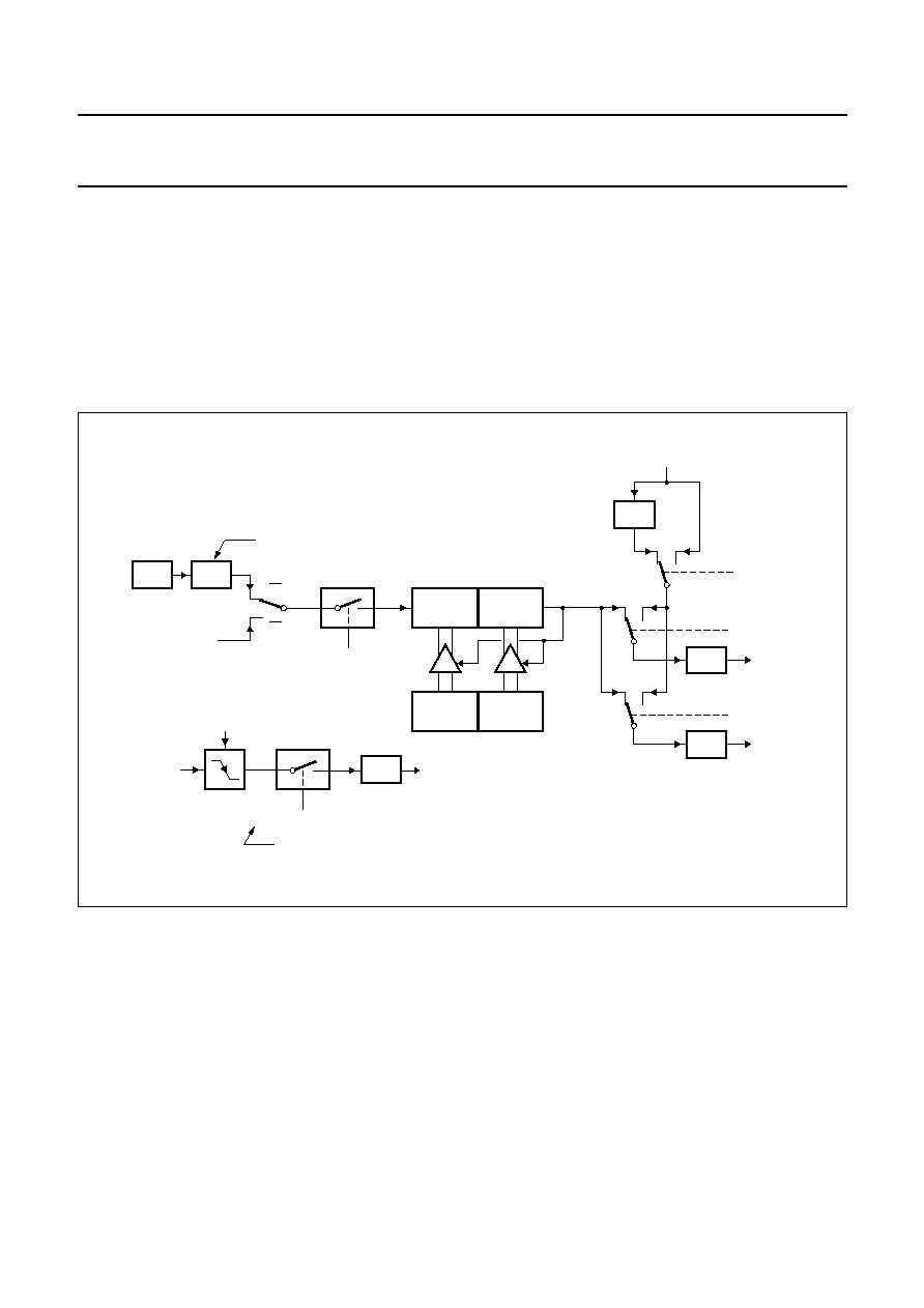
BLOCK DIAGRAM
TYPE NUMBER
PACKAGE
NAME
DESCRIPTION
VERSION
TDA8029HL/C1
LQFP32
plastic low profile quad flat package; 32 leads; body 7
◊
7
◊
1.4 mm
SOT358-1
TDA8029HL/C2
handbook, full pagewidth
XTAL
OSCILLATOR
80C51
CONTROLLER
16 kbytes ROM
256 bytes RAM
TIMER 2
512 bytes XRAM
SUPPLY
SUPERVISOR
DC/DC
CONVERTER
ANALOG
DRIVERS
AND
SEQUENCER
INTERNAL
OSCILLATOR
TDA8029
CLOCK
CIRCUITRY
24-bit
ETU
COUNTER
ISO 7816
UART
CONTROL/
STATUS
REGISTERS
SAM
VDD
SAP SBM
SBP
PGND
VUP
P32/INT0_N
P33/INT1_N
GND
220 nF
CDEL
DCIN
10
µ
F
CLK
RST
CS
P25
P37
P00/
P07
P20
VCC
GNDC
I/O
PRES
29
20
27
26
23
22
21
31
32
25
24
1
2
30
5
28
6
3
14
15
19
17
4
TEST
XTAL2
8
7
10
12
9
11
16
18
13
XTAL1
P16
P17
P27
P26
P30/RX
P31/TX
EA_N
ALE
PSEN_N
RESET
SDWN_N
FCE869
Fig.1 Block diagram.

2003 Oct 30
6
Philips Semiconductors
Product specification
Low power single card reader
TDA8029
7
PINNING
SYMBOL
PIN
DESCRIPTION
P17
1
general purpose I/O
P16
2
general purpose I/O; card clock generation up to 20 MHz with three times synchronous
frequency doubling (f
XTAL
,
1
/
2
f
XTAL
,
1
/
4
f
XTAL
and
1
/
8
f
XTAL
)
V
DD
3
supply voltage
GND
4
ground connection
SDWN_N
5
shut-down signal input; active LOW
CDEL
6
connection for an external capacitor determining the Power-on reset pulse width
(typically 1 ms per 2 nF)
I/O
7
data input/output to/from the card (C7); 14 k
integrated pull-up resistor to V
CC
PRES
8
card presence detection contact (active HIGH); do not connect to any external pull-up
or pull-down resistor; use with a normally open presence switch
GNDC
9
card ground (C5); connect to GND in the application
CLK
10
clock to the card (C3)
V
CC
11
card supply voltage (C1)
RST
12
card reset (C2)
VUP
13
output of the DC/DC converter (low ESR 220 nF to PGND)
SAP
14
DC/DC converter capacitor connection (low ESR 220 nF between SAP and SAM)
SBP
15
DC/DC converter capacitor connection (low ESR 220 nF between SBP and SBM)
DCIN
16
power input for the DC/DC converter
SBM
17
DC/DC converter capacitor connection (low ESR 220 nF between SBP and SBM)
PGND
18
ground for the DC/DC converter
SAM
19
DC/DC converter capacitor connection (low ESR 220 nF between SAP and SAM)
TEST
20
used for test purpose; connect to GND in the application
EA_N
21
control signal for microcontroller; connect to V
DD
in the application
ALE
22
control signal for the microcontroller; leave open in the application
PSEN_N
23
control signal for the microcontroller; leave open in the application
P27
24
general purpose I/O
P26
25
general purpose I/O
XTAL1
26
external crystal connection or input for an external clock signal
XTAL2
27
external crystal connection; leave open if an external clock is applied to XTAL1
RESET
28
reset input from the host (active HIGH); integrated pull-down resistor to GND
P32/INT0_N
29
interrupt signal from the smart card interface; leave open in the application
P33/INT1_N
30
external interrupt input or general purpose I/O; may be left open if not used
P31/TX
31
transmission line for serial communication with the host
P30/RX
32
reception line for serial communication with the host
2003 Oct 30
7
Philips Semiconductors
Product specification
Low power single card reader
TDA8029
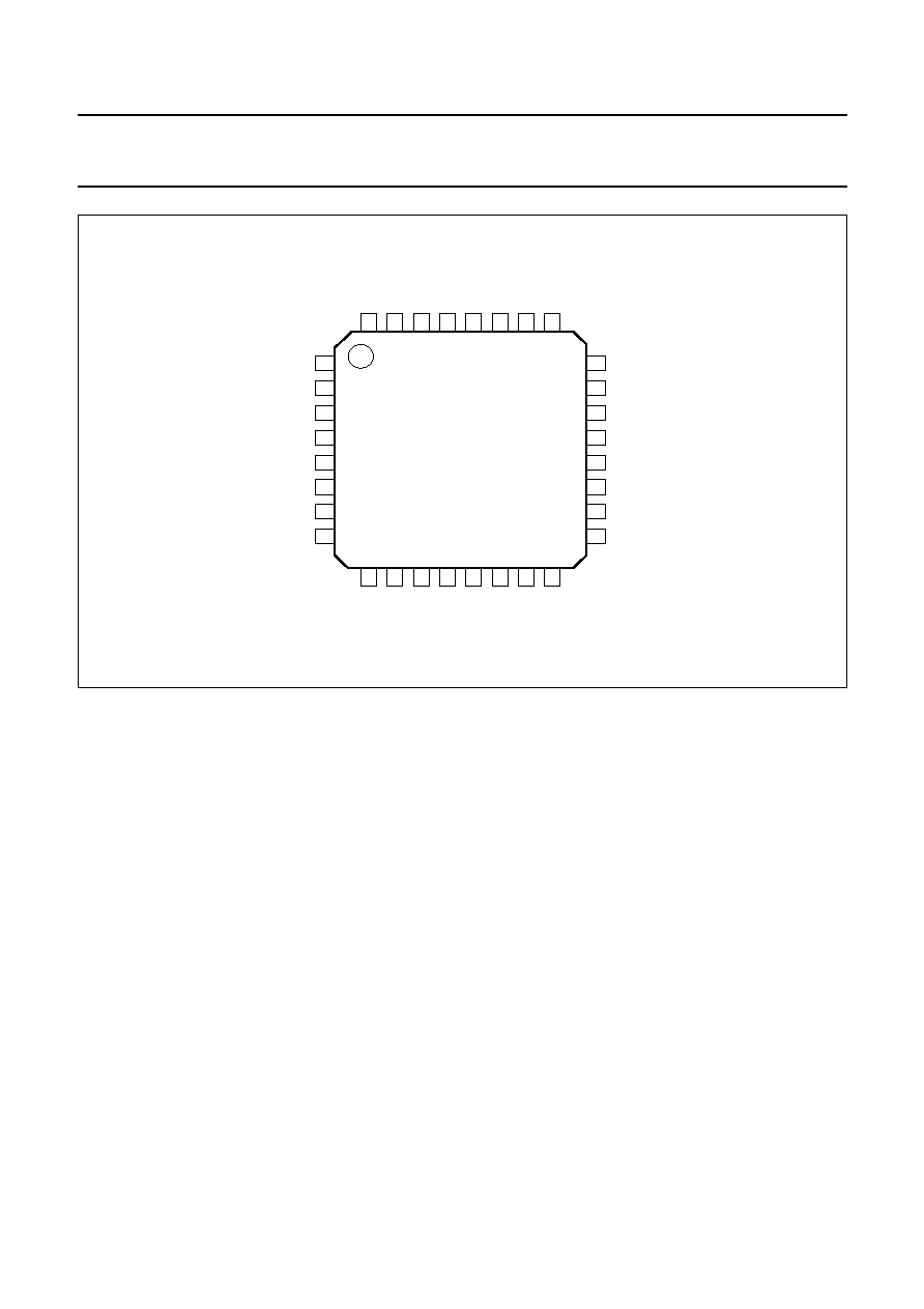
handbook, full pagewidth
TDA8029HL
FCE870
1
2
3
4
5
6
7
8
24
23
22
21
20
19
18
17
9
10
11
12
13
14
15
16
32
31
30
29
28
27
26
25
P17
P16
VDD
GND
SDWN_N
CDEL
I/O
PRES
P27
GNDC
CLK
V
CC
RST
VUP
SAP
SBP
DCIN
PSEN_N
ALE
EA_N
TEST
SAM
PGND
SBM
P26
XTAL1
XTAL2
RESET
P32/INT0_N
P33/INT1_N
P31/TX
P30/RX
Fig.2 Pin configuration.
8
FUNCTIONAL DESCRIPTION
Throughout this specification, it is assumed that the reader
is aware of ISO7816 norm terminology.
8.1
Microcontroller
The embedded microcontroller is an 80C51FB with
internal 16 kbytes ROM, 256 bytes RAM and 512 bytes
XRAM. It has the same instruction set as the 80C51.
The controller is clocked by the frequency present on pin
XTAL1.
The controller may be reset by an active HIGH signal on
pin RESET, but it is also reset by the Power-on reset signal
generated by the supply supervisor.
The external interrupt INT0_N is used by the ISO UART,
by the analog drivers and the ETU counters. It must be left
open in the application.
The second external interrupt INT1_N is available for the
application.
A general description as well as added features are
described in this chapter.
The added features to the 80C51 controller are similar to
the 8XC51FB controller, except on the wake-up from
Power-down mode, which is possible by a falling edge on
INT0_N (card reader problem) or on INT1_N or on RX due
to the addition of an extra delay counter and enable
configuration bits within register UCR2 (see detailed
description in Section 8.10.3.2). For any further
information please refer to the published specification of
the 8XC51FB in
"Data Handbook IC20; 80C51-Based 8-bit
Microcontrollers".
The controller has four 8-bit I/O ports, three 16-bit
timer/event counters, a multi-source, four-priority-level,
nested interrupt structure, an enhanced UART and on-chip
oscillator and timing circuits. For systems that require
extra memory capability up to 64 kbytes, it can be
expanded using standard TTL-compatible memories and
logic.

2003 Oct 30
8
Philips Semiconductors
Product specification
Low power single card reader
TDA8029
Additional features of the controller are:
∑
80C51 central processing unit
∑
Full static operation
∑
Security bits: ROM 2 bits
∑
Encryption array of 64 bits
∑
4-level priority structure
∑
6 interrupt sources
∑
Full-duplex enhanced UART with framing error
detection and automatic address recognition
∑
Power control modes; clock can be stopped and
resumed, Idle mode and Power-down mode
∑
Wake-up from Power-down by falling edge on INT0_N,
INT1_N and RX with an embedded delay counter
∑
Programmable clock out
∑
Second DPTR register
∑
Asynchronous port reset
∑
Low EMI by inhibit ALE.
Table 1 gives a list of main features to get a better
understanding of the differences between a standard
80C51, an 8XC51FB and the embedded controller in the
TDA8029.
Table 2 shows an overview of the special function
registers.
Table 1
Principal blocks in 80C51, 8XC51FB and TDA8029
FEATURE
80C51
8XC51FB
TDA8029
ROM
4 kbytes
16 kbytes
16 kbytes
RAM
128 bytes
256 bytes
256 bytes
ERAM (MOVX)
no
256 bytes
512 bytes
PCA
no
yes
no
WDT
no
yes
no
T0
yes
yes
yes
T1
yes
yes
yes
T2
no
yes
yes
lowest interrupt
priority-vector 002Bh
lowest interrupt
priority-vector 002Bh
4-level priority interrupt
no
yes
yes
enhanced UART
no
yes
yes
delay counter
no
no
yes

2003
Oct
30
9
Philips Semiconductors
Product specification
Lo
w po
w
er single card reader
TD
A8029
This text is here in white to force landscape pages to be rotated correctly when browsing through the pdf in the Acrobat reader.This text is here in
_
white to force landscape pages to be rotated correctly when browsing through the pdf in the Acrobat reader.This text is here inThis text is here in
white to force landscape pages to be rotated correctly when browsing through the pdf in the Acrobat reader. white to force landscape pages to be ...
Table 2
Embedded controller Special Function Registers (SFRs)
SYMBOL
DESCRIPTION
ADDR
(HEX)
BIT ADDRESS, SYMBOL OR ALTERNATIVE PORT FUNCTION
RESET
VALUE
(BINARY)
ACC
(1)
accumulator
E0
E7
E6
E5
E4
E3
E2
E1
E0
0000 0000
AUXR
(2)
auxiliary
8E
-
-
-
-
-
-
EXTRAM
AO
XXXX XX00
AUXR1
(2)
auxiliary
A2
-
-
-
LPEP
GF
0
-
DPS
XXX0 00X0
B
(1)
B register
F0
F7
F6
F5
F4
F3
F2
F1
F0
0000 0000
DPH
data pointer high 83
-
0000 0000
DPL
data pointer low
82
-
0000 0000
IE
(1)
interrupt enable
A8
EA
-
ET2
ES
ET1
EX1
ET0
EX0
0X00 0000
AF
AE
AD
AC
AB
AA
A9
A8
IP
(1)
interrupt priority
B8
-
-
PT2
PS
PT1
PX1
PT0
PX0
XX00 0000
BF
BE
BD
BC
BB
BA
B9
B8
IPH
(2)
interrupt priority
high
B7
-
-
PT2H
PSH
PT1H
PX1H
PT0H
PX0H
XX00 0000
P0
(1)
port 0
80
AD7
AD6
AD5
AD4
AD3
AD2
AD1
AD0
1111 1111
87
86
85
84
83
82
81
80
P1
(1)
port 1
90
-
-
-
-
-
-
T2EX
T2
1111 1111
97
96
95
94
93
92
91
90
P2
(1)
port 2
A0
A15
A14
A13
A12
A11
A10
A9
A8
1111 1111
A7
A6
A5
A4
A3
A2
A1
A0
P3
(1)
port 3
B0
RD
WR
T1
T0
INT1_N
INT0_N
TxD
RxD
1111 1111
B7
B6
B5
B4
B3
B2
B1
B0
PCON
(2)(3)
power control
87
SMOD1
SMOD0
-
POF
(4)
GF1
GF0
PD
IDL
00XX 0000
PSW
(1)
program status
word
D0
CY
AC
F0
RS1
RS0
OV
-
P
0000 00X0
D7
D6
D5
D4
D3
D2
D1
D0
RACAP2H
(2)
timer 2 capture
high
CB
-
0000 0000
RACAP2L
(2)
timer 2 capture
low
CA
-
0000 0000
SADDR
(2)
slave address
A9
-
0000 0000
SADEN
(2)
slave address
mask
B9
-
0000 0000
2003
Oct
30
10
Philips Semiconductors
Product specification
Lo
w po
w
er single card reader
TD
A8029
This text is here in white to force landscape pages to be rotated correctly when browsing through the pdf in the Acrobat reader.This text is here in
_
white to force landscape pages to be rotated correctly when browsing through the pdf in the Acrobat reader.This text is here inThis text is here in
white to force landscape pages to be rotated correctly when browsing through the pdf in the Acrobat reader. white to force landscape pages to be ...
Notes
1. Register is bit addressable.
2. Register is modified from or added to the 80C51 SFRs.
3. Reset value depends on reset source.
4. Bit will not be affected by reset.
SBUF
serial data buffer 99
-
XXXX XXXX
SCON
(1)
serial control
98
SM0/FE
SM1
SM2
REN
TB8
RB8
TI
RI
0000 0000
9F
9E
9D
9C
9B
9A
99
98
SP
stack pointer
81
-
0000 0111
TCON
(1)
timer control
88
TF1
TR1
TF0
TE0
IE1
IT1
IE0
IT0
0000 0000
8F
8E
8D
8C
8B
8A
89
88
T2CON
(1)
timer 2 control
C8
TF2
EXF2
RCLK
TCLK
EXEN2
TR2
C/T2
CP/RL2
0000 0000
CF
CE
CD
CC
CB
CA
C9
C8
T2MOD
(2)
timer 2 mode
control
C9
-
-
-
-
-
-
T2OE
DCEN
XXXX XX00
TH0
timer high 0
8C
-
0000 0000
TH1
timer high 1
8D
-
0000 0000
TH2
(2)
timer high 2
CD
-
0000 0000
TL0
timer low 0
8A
-
0000 0000
TL1
timer low 1
8B
-
0000 0000
TL2
(2)
timer low 2
CC
-
0000 0000
TMOD
timer mode
89
GATE
C/T
M1
M0
GATE
C/T
M1
M0
0000 0000
SYMBOL
DESCRIPTION
ADDR
(HEX)
BIT ADDRESS, SYMBOL OR ALTERNATIVE PORT FUNCTION
RESET
VALUE
(BINARY)

2003 Oct 30
11
Philips Semiconductors
Product specification
Low power single card reader
TDA8029
8.1.1
P
ORT CHARACTERISTICS
Port 0 (P0.7 to P0.0): Port 0 is an open-drain,
bidirectional, I/O timer 2 generated commonly used baud
rates port. Port 0 pins that have logic 1s written to them
float and can be used as high-impedance inputs. Port 0 is
also the multiplexed low-order address and data bus
during access to external program and data memory.
In this application, it uses strong internal pull-ups when
emitting logic 1s. Port 0 also outputs the code bytes during
program verification and received code bytes during
EPROM programming. External pull-ups are required
during program verification.
Port 1 (P1.7 to P1.0): Port 1 is an 8-bit bidirectional
I/O-port with internal pull-ups. Port 1 pins that have
logic 1s written to them are pulled to HIGH level by the
internal pull-ups and can be used as inputs. As inputs,
port 1 pins that are externally pulled LOW will source
current because of the internal pull-ups. Port 1 also
receives the low-order address byte during program
memory verification. Alternate functions for port 1 include:
∑
T2 (P1.0): Timer/counter 2 external count input / clock
out (see programmable clock out)
∑
T2EX (P1.1): Timer/counter 2 reload/capture/direction
control.
Port 2 (P2.7 to P2.0): Port 2 is an 8-bit bidirectional I/O
port with internal pull-ups. Port 2 pins that have logic 1s
written to them are pulled to HIGH level by the internal
pull-ups and can be used as inputs. As inputs, port 2 pins
that are externally being pulled to LOW will source current
because of the internal pull-ups. Port 2 emits the
high-order address byte during fetches from external
program memory and during access to external data
memory that use 16-bit addresses (MOVX @DPTR). In
this application, it uses strong internal pull-ups when
emitting logic 1s. During access to external data memory
that use 8-bit addresses (MOV @Ri), port 2 emits the
contents of the P2 special function register. Some port 2
pins receive the high order address bits during EPROM
programming and verification.
Port 3 (P3.7 to P3.3, P3.1 and P3.0): Port 3 is a 7-bit
bidirectional I/O port with internal pull-ups. Port 3 pins that
have logic 1s written to them are pulled to HIGH level by
the internal pull-ups and can be used as inputs. As inputs,
port 3 pins that are externally being pulled LOW will source
current because of the pull-ups.
Port 3 also serves the special features of the 80C51 family:
∑
RxD (P3.0): Serial input port
∑
TxD (P3.1): Serial output port
∑
INT0 (P3.2): External interrupt 0 (pin INT0_N)
∑
INT1 (P3.3): External interrupt 1 (pin INT1_N
∑
T0 (P3.4): Timer 0 external input
∑
T1 (P3.5): Timer 1 external input
∑
WR (P3.6): External data memory write strobe
∑
RD (P3.7): External data memory read strobe.
8.1.2
O
SCILLATOR CHARACTERISTICS
XTAL1 and XTAL2 are the input and output, respectively,
of an inverting amplifier. The pins can be configured for
use as an on-chip oscillator. To drive the device from an
external clock source, XTAL1 should be driven while
XTAL2 is left unconnected. There are no requirements on
the duty cycle of the external clock signal, because the
input to the internal clock circuitry is through a
divide-by-two flip-flop. However, minimum and maximum
HIGH and LOW times specified must be observed.
8.1.3
R
ESET
The microcontroller is reset when the TDA8029 is reset, as
described in Section 8.11.
8.1.4
L
OW POWER MODES
This section describes the low power modes of the
microcontroller. Please refer to Section 8.15 for additional
information of the TDA8029 power reduction modes.
Stop clock mode: The static design enables the clock
speed to be reduced down to 0 MHz (stopped). When the
oscillator is stopped, the RAM and special function
registers retain their values. This mode allows
step-by-step utilization and permits reduced system power
consumption by lowering the clock frequency down to any
value. For lowest power consumption the Power-down
mode is suggested.
Idle mode: In the Idle mode, the CPU puts itself to sleep
while all of the on-chip peripherals stay active. The
instruction to invoke the Idle mode is the last instruction
executed in the normal operating mode before the Idle
mode is activated. The CPU contents, the on-chip RAM,
and all of the special function registers remain intact during
2003 Oct 30
12
Philips Semiconductors
Product specification
Low power single card reader
TDA8029
this mode. The Idle mode can be terminated either by any
enabled interrupt (at which time the process is picked up
at the interrupt service routine and continued), or by a
hardware reset which starts the processor in the same
manner as a Power-on reset.
Power-down mode: To save even more power, a
Power-down mode can be invoked by software. In this
mode, the oscillator is stopped and the instruction that
invoked Power-down is the last instruction executed.
Either a hardware reset, external interrupt or reception
on RX can be used to exit from Power-down mode. Reset
redefines all the SFRs but does not change the on-chip
RAM. An external interrupt allows both the SFRs and the
on-chip RAM to retain their values.
With INT0_N, INT1_N or RX, the bits in register IE must be
enabled. Within the INT0_N interrupt service routine, the
controller has to read out the Hardware Status Register
(HSR @ 0Fh) and/or the UART Status register
(USR @ 0Eh) by means of MOVX-instructions in order to
know the exact interrupt reason and to reset the interrupt
source.
For enabling a wake up by INT1_N, the bit ENINT1 within
UCR2 must be set.
For enabling a wake up by RX, the bits ENINT1 and ENRX
within UCR2 must be set.
An integrated delay counter maintains internally INT0_N
and INT1_N LOW long enough to allow the oscillator to
restart properly, so a falling edge on pins RX, INT0_N and
INT1_N is enough for awaking the whole circuit.
Once the interrupt is serviced, the next instruction to be
executed after RETI will be the one following the
instruction that put the device into power-down.
Table 3
External pin status during Idle and Power-down mode
MODE
PROGRAM MEMORY
ALE
PSEN_N
PORT 0
PORT 1
PORT 2
PORT 3
Idle
internal
1
1
data
data
data
data
external
1
1
float
data
address
data
Power-down
internal
0
0
data
data
data
data
external
0
0
float
data
data
data

2003 Oct 30
13
Philips Semiconductors
Product specification
Low power single card reader
TDA8029
8.2
Timer 2 operation
Timer 2 is a 16-bit timer and counter which can operate as either an event timer or an event counter, as selected by bit
C/T2 in the special function register T2CON. Timer 2 has three operating modes: capture, auto-reload (up-or down
counting), and baud rate generator, which are selected by bits in register T2CON.
8.2.1
T
IMER
/
COUNTER
2 C
ONTROL REGISTER
(T2CON)
Table 4
Timer/counter 2 control register bits
Table 5
Description of register bits
Table 6
Timer 2 operating modes
BIT
7
6
5
4
3
2
1
0
Symbol
TF2
EXF2
RCLK
TCLK
EXEN2
TR2
C/T2
CP/RL2
BIT
SYMBOL
DESCRIPTION
7
TF2
Timer 2 overflow flag. Set by a timer 2 overflow and must be cleared by software. TF2
will not be set when either RCLK = 1 or TCLK = 1.
6
EXF2
Timer 2 external flag. Set when either a capture or reload is caused by a negative
transition on controller input T2EX and EXEN2 = 1. When timer 2 interrupt is enabled,
EXF2 = 1 will cause the CPU to vector to the timer 2 interrupt routine. EXF2 must be
cleared by software. EXF2 does not cause an interrupt in up- or down-counter mode
(DCEN = 1).
5
RCLK
Receive clock flag. When set, causes the serial port to use timer 2 overflow pulses for
its receive clock in modes 1 and 3. When reset, causes timer 1 overflow to be used for
the receive clock.
4
TCLK
Transmit clock flag. When set, causes the serial port to use timer 2 overflow pulses for
its transmit clock in modes 1 and 3. When reset, causes timer 1 overflows to be used for
the transmit clock.
3
EXEN2
Timer 2 external enable flag. When set, allows a capture or reload to occur as a result
of a negative transition on T2EX if timer 2 is not being used to clock the serial port. When
reset, causes timer 2 to ignore events at T2EX.
2
TR2
Start/stop control for timer 2. TR2 = 1 starts the timer.
1
C/T2
Counter or Timer select timer 2. If C/T2 = 0 the internal timer at
1
/
12
f
XTAL1
is selected;
C/T2 = 1 selects the external event counter (falling edge triggered).
0
CP/RL2
Capture or reload flag. When set, captures will occur on negative transitions at T2EX if
EXEN2 = 1. When reset, auto-reloads will occur either with timer 2 overflows or negative
transitions at T2EX when EXEN2 = 1. When either RCLK = 1 or TCLK = 1, this bit is
ignored and the timer is forced to auto-reload on timer 2 overflow.
MODE
RCLK AND TCLK
CP/RL2
TR2
16-bit auto-reload
0
0
1
Baud rate generator
1
X
1
Off
X
X
0

2003 Oct 30
14
Philips Semiconductors
Product specification
Low power single card reader
TDA8029
8.2.2
T
IMER
/
COUNTER
2 M
ODE CONTROL REGISTER
(T2MOD)
Table 7
Timer/counter 2 mode control register bits
Table 8
Description of register bits
Note
1. Do not write logic 1s to reserved bits. These bits may be used in future 80C51 family products to invoke new features.
In that case, the reset or inactive value of the new bit will be logic 0, and its active value will be logic 1. The value
read from a reserved bit is indeterminate.
BIT
7
6
5
4
3
2
1
0
Symbol
-
-
-
-
-
-
T2OE
DCEN
BIT
SYMBOL
DESCRIPTION
7 to 2
-
Not implemented. Reserved for future use; note 1.
1
T2OE
Timer 2 Output Enable.
0
DCEN
Down Counter Enable. When set, allows timer 2 to be configured as up-/down-counter.
8.2.3
A
UTO
-
RELOAD MODE
(
UP
-
OR DOWN
-
COUNTER
)
In the 16-bit auto-reload mode, timer 2 can be configured
as either a timer or counter (bit C/T2 in register T2CON)
and programmed to count up or down. The counting
direction is determined by bit DCEN (down-counter
enable) which is located in the T2MOD register. When
reset, DCEN = 0 and timer 2 will default to counting up. If
DCEN = 1, timer 2 can count up or down depending on the
value of T2EX.
When DCEN = 0, timer 2 will count up automatically.
In this mode there are two options selected by bit EXEN2
in register T2CON. If EXEN2 = 0, then timer 2 counts up to
0FFFFh and sets the TF2 overflow flag upon overflow.
This causes the timer 2 registers to be reloaded with the
16-bit value in RCAP2L and RCAP2H. The values in
RCAP2L and RCAP2H are preset by software. If
EXEN2 = 1, then a 16-bit reload can be triggered either by
an overflow or by a HIGH to LOW transition at controller
input T2EX. This transition also sets the EXF2 bit. The
timer 2 interrupt, if enabled, can be generated when either
TF2 or EXF2 are logic 1. See Fig.3 for an overview.
DCEN = 1 enables timer 2 to count up- or down. This
mode allows T2EX to control the direction of count. When
a HIGH level is applied at T2EX timer 2 will count up.
Timer 2 will overflow at 0FFFFh and set the TF2 flag,
which can then generate an interrupt, if the interrupt is
enabled. This timer overflow also causes the 16-bit value
in RCAP2L and RCAP2H to be reloaded into the timer
registers TL2 and TH2. When a LOW level is applied at
T2EX this causes timer 2 to count down. The timer will
underflow when TL2 and TH2 become equal to the value
stored in RCAP2L and RCAP2H. Timer 2 underflow sets
the TF2 overflow flag and causes 0FFFFh to be reloaded
into the timer registers TL2 and TH2. See Fig.4 for an
overview.
The external flag EXF2 toggles when timer 2 underflows or
overflows. This EXF2 bit can be used as a 17th bit of
resolution if needed. The EXF2 flag does not generate an
interrupt in this mode of operation.
2003 Oct 30
15
Philips Semiconductors
Product specification
Low power single card reader
TDA8029
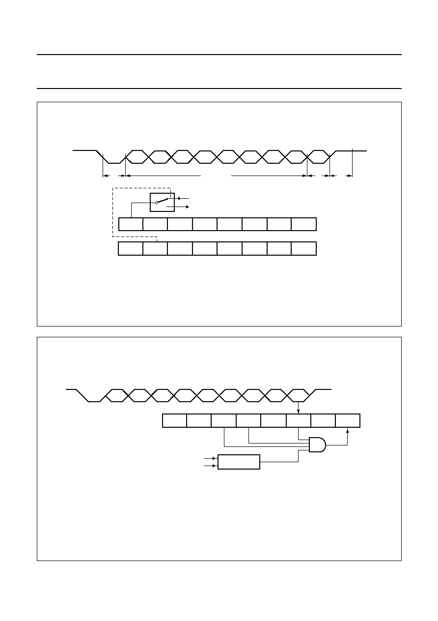
handbook, full pagewidth
˜
12
MGW423
TR2
TL2
(8-bit)
TH2
(8-bit)
RCAP2L
TF2
EXF2
RCAP2H
C/T2 = 0
C/T2 = 1
T2
reload
transition
detector
control
control
Timer 2
interrupt
T2EX
EXEN2
OSC
Fig.3 Timer 2 in auto-reload mode with DCEN = 0.
handbook, full pagewidth
˜
12
MGW424
TR2
TL2
TH2
RCAP2L
TF2
RCAP2H
FFh
FFh
C/T2 = 0
C/T2 = 1
T2
overflow
toggle
control
interrupt
count
direction
HIGH = up
LOW = down
T2EX
(up counting reload value)
(down counting reload value)
EXF2
OSC
Fig.4 Timer 2 in auto-reload mode with DCEN = 1.

2003 Oct 30
16
Philips Semiconductors
Product specification
Low power single card reader
TDA8029
8.2.4
B
AUD RATE GENERATOR MODE
Bits TCLK and/or RCLK in register T2CON allow the serial
port transmit and receive baud rates to be derived from
either timer 1 or 2. When TCLK = 0, timer 1 is used as the
serial port transmit baud rate generator. When TCLK = 1,
timer 2 is used. RCLK has the same effect for the serial
port receive baud rate. With these two bits, the serial port
can have different receive and transmit baud rates, one
generated by timer 1, the other by timer 2.
The baud rate generation mode is like the auto-reload
mode, in that a rollover in TH2 causes the timer 2 registers
to be reloaded with the 16-bit value in registers RCAP2H
and RCAP2L, which are preset by software.
The baud rates in modes 1 and 3 are determined by the
overflow rate of timer 2, given by equation (1):
(1)
The timer can be configured for either timer or counter
operation. In many applications, it is configured for timer
operation (C/T2 = 0). Timer operation is different for
timer 2 when it is being used as a baud rate generator.
Usually, as a timer it would increment every machine cycle
(i.e.
1
/
12
f
osc
). As a baud rate generator, it increments every
state time (i.e.
1
/
2
f
osc
). Thus the modes 1 and 3 baud rate
formula is as Equation (2):
(2)
Where (RCAP2H, RCAP2L) is the contents of RCAP2H
and RCAP2L registers taken as a 16-bit unsigned integer.
The timer 2 as a baud rate generator is valid only if
RCLK = 1 and/or TCLK = 1 in the T2CON register. Note
that a rollover in TH2 does not set TF2, and will not
generate an interrupt. Thus, the timer 2 interrupt does not
have to be disabled when timer 2 is in the baud rate
generator mode. Also if the EXEN2 (T2 external enable)
flag is set, a HIGH to LOW transition on T2EX
(Timer/counter 2 trigger input) will set the EXF2 (T2
external) flag but will not cause a reload from (RCAP2H
and RCAP2L) to (TH2 and TL2). Therefore, when timer 2
is used as a baud rate generator, T2EX can be used as an
additional external interrupt, if needed.
When timer 2 is in the baud rate generator mode, never try
to read or write TH2 and TL2. As a baud rate generator,
timer 2 is incremented every state time (
1
/
2
f
osc
) or
asynchronously from controller I/O T2; under these
conditions, a read or write of TH2 or TL2 may not be
accurate. The RCAP2 registers may be read, but should
not be written to, because a write might overlap a reload
and cause write and/or reload errors. The timer should be
turned off (clear TR2) before accessing the timer 2 or
RCAP2 registers. See Fig.5 for an overview.
Baud rate
Timer 2 overflow rate
16
--------------------------------------------------------
=
Baud rate
Oscillator frequency
32
65536
RCAP2H, RCAP2L
(
)
≠
[
]
◊
------------------------------------------------------------------------------------------------
=
Table 9
Timer 2 generated commonly used baud rates
BAUD RATE
CRYSTAL OSCILLATOR
FREQUENCY
TIMER
RCAP2H (HEX)
RCAP2L (HEX)
375k
12 MHz
FF
FF
9.6k
12 MHz
FF
D9
2.8k
12 MHz
FF
B2
2.4k
12 MHz
FF
64
1.2k
12 MHz
FE
C8
300
12 MHz
FB
1E
110
12 MHz
F2
AF
300
6 MHz
FD
8F
110
6 MHz
F9
57
2003 Oct 30
17
Philips Semiconductors
Product specification
Low power single card reader
TDA8029
Summary of baud rate equations: Timer 2 is in baud rate
generating mode. If timer 2 is being clocked through T2
(P1.0) the baud rate is:
(3)
If timer 2 is being clocked internally, the baud rate is:
(4)
To obtain the reload value for RCAP2H and RCAP2L, the
above equation can be rewritten as:
(5)
Where f
osc
= oscillator frequency.
Baud rate
Timer 2 overflow rate
16
--------------------------------------------------------
=
Baud rate
Oscillator frequency
32
65536
RCAP2H, RCAP2L
(
)
≠
[
]
◊
------------------------------------------------------------------------------------------------
=
RCAP2H, RCAP2L
65536
f
osc
32
baud rate
◊
--------------------------------------
≠
=
handbook, full pagewidth
MGW425
TR2
TL2
(8-bit)
TH2
(8-bit)
RCAP2L
EXF2
RCAP2H
reload
SMOD
RCLK
TCLK
1
0
0
Timer 1
overflow
1
1
0
transition
detector
control
control
Note availability of additional external interrupt
note fosc is divided by 2, not 12
Timer 2
interrupt
RX clock
T2EX
EXEN2
˜
2
˜
16
TX clock
˜
16
˜
2
C/T2 = 0
C/T2 = 1
T2
OSC
Fig.5 Timer 2 in baud rate generator mode.
2003 Oct 30
18
Philips Semiconductors
Product specification
Low power single card reader
TDA8029
8.2.5
T
IMER
/
COUNTER
2
SET
-
UP
Except for the baud rate generator mode, the values given for T2CON do not include the setting of the TR2 bit. Therefore,
bit TR2 must be set, separately, to turn the timer on.
Table 10 Timer 2 as a timer
Notes
1. Capture/reload occurs only on timer/counter overflow.
2. Capture/reload on timer/counter overflow and a HIGH to LOW transition on T2EX, except when timer 2 is used in the
baud rate generator mode.
Table 11 Timer 2 as a counter
Notes
1. Capture/reload occurs only on timer/counter overflow.
2. Capture/reload on timer/counter overflow and a HIGH to LOW transition on T2EX (P1.1) pin except when timer 2 is
used in the baud rate generator mode.
8.3
Enhanced UART
The UART operates in all of the usual modes that are described in the first section of "
Data Handbook IC20,
80C51-based 8-bit microcontrollers". In addition the UART can perform framing error detection by looking for missing
stop bits and automatic address recognition. The UART also fully supports multiprocessor communication as does the
standard 80C51 UART.
When used for framing error detection the UART looks for missing stop bits in the communication. A missing bit will set
the bit FE or bit 7 in the SCON register. Bit FE is shared with bit SM0. The function of SCON bit 7 is determined by bit 6
in register PCON (bit SMOD0). If SMOD0 is set then bit 7 of register SCON functions as FE and as SM0 when SMOD0
is cleared. When used as FE this bit can only be cleared by software.
8.3.1
S
ERIAL PORT
C
ONTROL REGISTER
(SCON)
Table 12 Serial port control register bits
MODE
T2CON
INTERNAL CONTROL
(1)
(HEX)
EXTERNAL CONTROL
(2)
(HEX)
16-bit auto-reload
00
08
Baud rate generator receive and
transmit same baud rate
34
36
Receive only
24
26
Transmit only
14
16
MODE
T2CON
INTERNAL CONTROL
(1)
(HEX)
EXTERNAL CONTROL
(2)
(HEX)
16-bit
02
04
Auto-reload
03
0B
BIT
7
6
5
4
3
2
1
0
Symbol
SM0/FE
SM1
SM2
REN
TB8
RB8
TI
RI

2003 Oct 30
19
Philips Semiconductors
Product specification
Low power single card reader
TDA8029
Table 13 Description of register bits
Table 14 Enhanced UART modes
BIT
SYMBOL
DESCRIPTION
7
SM0/FE
The function of this bit is determined by SMOD0, bit 6 of register PCON. If SMOD0 is set
then this bit functions as FE. This bit functions as SM0 when SMOD0 is reset. When
used as FE, this bit can only be cleared by software.
SM0: Serial port mode bit 0. See Table 14.
FE: Framing Error bit. This bit is set by the receiver when an invalid stop bit is
detected; see Fig.6. The FE bit is not cleared by valid frames but should be cleared by
software. The SMOD0 bit in register PCON must be set to enable access to FE.
6
SM1
Serial port mode bit 1. See Table 14.
5
SM2
Serial port mode bit 2. Enables the automatic address recognition feature in modes
2 or 3. If SM2 = 1, bit Rl will not be set unless the received 9th data bit (RB8) is logic 1;
indicating an address and the received byte is a given or broadcast address. In mode 1,
if SM2 = 1 then Rl will not be activated unless a valid stop bit was received, and the
received byte is a given or broadcast address. In mode 0, SM2 should be logic 0.
4
REN
Enables serial reception. Set by software to enable reception. Cleared by software to
disable reception.
3
TB8
The 9th data bit transmitted in modes 2 and 3. Set or cleared by software as desired.
In mode 0, TB8 is not used.
2
RB8
The 9th data bit received in modes 2 and 3. In mode 1, if SM2 = 0, RB8 is the stop bit
that was received. In mode 0, RB8 is not used.
1
Tl
Transmit interrupt flag. Set by hardware at the end of the 8th bit time in mode 0, or at
the beginning of the stop bit in the other modes, in any serial transmission. Must be
cleared by software.
0
Rl
Receive interrupt flag. Set by hardware at the end of the 8th bit time in mode 0, or
halfway through the stop bit time in the other modes, in any serial reception (except if
SM2 = 1, as described for SM2). Must be cleared by software.
SM0
SM1
MODE
DESCRIPTION
BAUD RATE
0
0
0
shift register
1
/
12
f
XTAL1
0
1
1
8-bit UART
variable
1
0
2
9-bit UART
1
/
32
or
1
/
64
f
XTAL1
1
1
3
9-bit UART
variable
8.3.2
A
UTOMATIC ADDRESS RECOGNITION
Automatic address recognition is a feature which allows
the UART to recognize certain addresses in the serial bit
stream by using hardware to make the comparisons. This
feature saves a great deal of software overhead by
eliminating the need for the software to examine every
serial address which passes by the serial port. This feature
is enabled by setting the SM2 bit in register SCON. In the
9-bit UART modes (modes 2 and 3), the Receive Interrupt
flag (RI) will be automatically set when the received byte
contains either the `given' address or the `broadcast'
address. The 9-bit mode requires that the 9th information
bit is a logic 1 to indicate that the received information is an
address and not data. Figure 7 gives a summary.
The 8-bit mode is called mode 1. In this mode the RI flag
will be set if SM2 is enabled and the information received
has a valid stop bit following the 8 address bits and the
information is either a given or a broadcast address.
Mode 0 is the Shift Register mode and SM2 is ignored.
Using the automatic address recognition feature allows a
master to selectively communicate with one or more
slaves by invoking the given slave address or addresses.
All of the slaves may be contacted by using the broadcast

2003 Oct 30
20
Philips Semiconductors
Product specification
Low power single card reader
TDA8029
address. Two special function registers are used to define
the slave addresses, SADDR, and the address mask,
SADEN. SADEN is used to define which bits in the SADDR
are to be used and which bits are `don't cares'. The
SADEN mask can be logically AND-ed with the SADDR to
create the given address which the master will use for
addressing each of the slaves. Use of the given address
allows multiple slaves to be recognized while excluding
others. The following examples will help to show the
versatility of this scheme.
Table 15 Slave 0
Table 16 Slave 1
In the above example SADDR is the same and the SADEN
data is used to differentiate between the two slaves.
Slave 0 requires that bit 0 = 0 and ignores bit 1. Slave 1
requires that bit 1 = 0 and bit 0 is ignored. A unique
address for slave 0 would be 1100 0010 since slave 1
requires bit 1 = 0. A unique address for slave 1 would be
1100 0001 since bit 0 = 1 will exclude slave 0. Both slaves
can be selected at the same time by an address which has
bit 0 = 0 (for slave 0) and bit 1 = 0 (for slave 1). Thus, both
could be addressed with 1100 0000.
In a more complex system the following could be used to
select slaves 1 and 2 while excluding slave 0.
Table 17 Slave 0
Table 18 Slave 1
Table 19 Slave 2
In the above example the differentiation among the
3 slaves is in the lower 3 address bits. Slave 0 requires
that bit 0 = 0 and it can be uniquely addressed by
1110 0110. Slave 1 requires that bit 1 = 0 and it can be
uniquely addressed by 1110 and 0101. Slave 2 requires
that bit 2 = 0 and its unique address is 1110 0011.
To select slaves 0 and 1 and exclude slave 2 use address
1110 0100, since it is necessary to make bit 2 = 1 to
exclude slave 2.
The broadcast address for each slave is created by taking
the logical OR of SADDR and SADEN. Zeros in this result
are treated as don't cares. In most cases, interpreting the
don't cares as ones, the broadcast address will be FFh.
Upon reset SADDR (SFR address 0A9h) and SADEN
(SFR address 0B9h) are leaded with 0s. This produces a
given address of all `don't cares' as well as a broadcast
address of all `don't cares'. This effectively disables the
automatic addressing mode and allows the microcontroller
to use standard 80C51 type UART drivers which do not
make use of this feature.
REGISTER
VALUE (BINARY)
SADDR
1100 0000
SADEN
1111 1101
Given
1100 00X0
REGISTER
VALUE (BINARY)
SADDR
1100 0000
SADEN
1111 1110
Given
1100 000X
REGISTER
VALUE (BINARY)
SADDR
1100 0000
SADEN
1111 1001
Given
1100 0XX0
REGISTER
VALUE (BINARY)
SADDR
1110 0000
SADEN
1111 1010
Given
1110 0X0X
REGISTER
VALUE (BINARY)
SADDR
1110 0000
SADEN
1111 1100
Given
1110 00XX
2003 Oct 30
21
Philips Semiconductors
Product specification
Low power single card reader
TDA8029
handbook, full pagewidth
MDB816
SM0/FE
SM1
SM2
REN
TB8
RB8
TI
RI
SMOD1
SMOD0
0 : SCON.7 = SM0
1 : SCON.7 = FE
-
POF
GF1
GF0
PD
IDL
SCON
(98h)
PCON
(87h)
Set FE bit if STOP bit is 0 (framing error)
SM0 to UART mode control
D0
D1
D2
D3
D4
D5
D6
D7
D8
START
bit
DATA byte
only
in
MODE 2, 3
STOP
bit
Fig.6 UART framing error detection.
handbook, full pagewidth
MDB817
SM0
SM1
SM2
REN
TB8
1
1
1
1
X
1
0
COMPARATOR
RB8
TI
RI
SCON
(98h)
D0
D1
D2
D3
D4
D5
D6
D7
D8
received address D0 to D7
programmed address
Fig.7 UART multiprocessor communication, automatic address recognition.
UART modes 2 or 3 and SM2 = 1: there is an interrupt if REN = 1, RB8 = 1 and received address is equal to programmed address.
When own address is received, reset SM2 to receive the data bytes. When all data bytes are received, set SM2 to wait for the next address.

2003 Oct 30
22
Philips Semiconductors
Product specification
Low power single card reader
TDA8029
8.4
Interrupt priority structure
The TDA8029 has a 6-source 4-level interrupt structure.
There are three SFRs associated with the 4-level interrupt: IE, IP and IPH. The Interrupt Priority High (IPH) register
implements the 4-level interrupt structure. The IPH is located at SFR address B7h.
The function of the IPH is simple and when combined with the IP determines the priority of each interrupt. The priority of
each interrupt is determined as shown in Table 20.
Table 20 Priority bits
Table 21 Interrupt table
Notes
1. Level activated.
2. Transition activated.
8.4.1
I
NTERRUPT
E
NABLE
(IE)
REGISTER
Table 22 Interrupt enable register bits
Table 23 Description of register bits
IPH BIT n
IP BIT n
INTERRUPT PRIORITY LEVEL
0
0
level 0 (lowest priority)
0
1
level 1
1
0
level 2
1
1
level 3 (highest priority)
SOURCE
POLLING PRIORITY
REQUEST BITS
HARDWARE CLEAR
VECTOR ADDRESS
(HEX)
X0
1
IE0
N
(1)
; Y
(2)
03
T0
2
TF0
Y
0B
X1
3
IE1
N
(1)
; Y
(2)
13
T1
4
TF1
Y
1B
SP
5
RI, TI
N
23
T2
6
TF2, EXF2
N
2B
BIT
7
6
5
4
3
2
1
0
Symbol
EA
-
ET2
ES
ET1
EX1
ET0
EX0
BIT
SYMBOL
DESCRIPTION
(1)
7
EA
Global disable. If EA = 0, all interrupts are disabled; If EA = 1, each interrupt can be
individually enabled or disabled by setting or clearing its enable bit.
6
-
Not implemented. Reserved for future use; note 2.
5
ET2
Timer 2 interrupt enable. ET2 = 1 enables the interrupt; ET2 = 0 disables the interrupt.
4
ES
Serial port interrupt enable. ES = 1 enables the interrupt; ES = 0 disables the interrupt.
3
ET1
Timer 1 interrupt enable. ET1 = 1 enables the interrupt; ET1 = 0 disables the interrupt.
2003 Oct 30
23
Philips Semiconductors
Product specification
Low power single card reader
TDA8029
Notes
1. Details on interaction with the UART behaviour in Power-down mode are described in Section 8.15.
2. Do not write logic 1s to reserved bits. These bits may be used in future 80C51 family products to invoke new features.
In that case, the reset or inactive value of the new bit will be logic 0, and its active value will be logic 1. The value
read from a reserved bit is indeterminate.
8.4.2
I
NTERRUPT
P
RIORITY
(IP)
REGISTER
Table 24 Interrupt priority register bits
Table 25 Description of register bits
Note
1. Do not write logic 1s to reserved bits. These bits may be used in future 80C51 family products to invoke new features.
In that case, the reset or inactive value of the new bit will be logic 0, and its active value will be logic 1. The value
read from a reserved bit is indeterminate.
8.4.3
I
NTERRUPT
P
RIORITY
H
IGH
(IPH)
REGISTER
Table 26 Interrupt priority high register bits
Table 27 Description of register bits
2
EX1
External interrupt 1 enable. EX1 = 1 enables the interrupt; EX1 = 0 disables the
interrupt.
1
ET0
Timer 0 interrupt enable. ET0 = 1 enables the interrupt; ET0 = 0 disables the interrupt.
0
EX0
External interrupt 0 enable. EX0 = 1 enables the interrupt; EX0 = 0 disables the
interrupt.
BIT
7
6
5
4
3
2
1
0
Symbol
-
-
PT2
PS
PT1
PX1
PT0
PX0
BIT
SYMBOL
DESCRIPTION
7 and 6
-
Not implemented. Reserved for future use; note 1.
5
PT2
Timer 2 interrupt priority. See Table 20.
4
PS
Serial port interrupt priority. See Table 20.
3
PT1
Timer 1 interrupt priority. See Table 20.
2
PX1
External interrupt 1 priority. See Table 20.
1
PT0
Timer 0 interrupt priority. See Table 20.
0
PX0
External interrupt 0 priority. See Table 20.
BIT
7
6
5
4
3
2
1
0
Symbol
-
-
PT2H
PSH
PT1H
PX1H
PT0H
PX0H
BIT
SYMBOL
DESCRIPTION
7 and 6
-
Not implemented. Reserved for future use; note 1.
5
PT2H
Timer 2 interrupt priority. See Table 20.
4
PSH
Serial port interrupt priority. See Table 20.
3
PT1H
Timer 1 interrupt priority. See Table 20.
BIT
SYMBOL
DESCRIPTION
(1)

2003 Oct 30
24
Philips Semiconductors
Product specification
Low power single card reader
TDA8029
Note
1. Do not write logic 1s to reserved bits. These bits may be used in future 80C51 family products to invoke new features.
In that case, the reset or inactive value of the new bit will be logic 0, and its active value will be logic 1. The value
read from a reserved bit is indeterminate.
2
PX1H
External interrupt 1 priority. See Table 20.
1
PT0H
Timer 0 interrupt priority. See Table 20.
0
PX0H
External interrupt 0 priority. See Table 20.
BIT
SYMBOL
DESCRIPTION
8.5
Dual Data Pointer (DPTR)
The dual DPTR structure is a way by which the TDA8029
will specify the address of an external data memory
location. There are two 16-bit DPTR registers that address
the external memory, and a single bit called DPS (bit 0 of
the AUXR1 register) that allows the program code to
switch between them.
The DPS bit should be saved by software when switching
between DPTR0 and DPTR1.
The GF bit (bit 2 in register AUXR1) is a general purpose
user-defined flag. Note that bit 2 is not writable and is
always read as a logic 0. This allows the DPS bit to be
quickly toggled simply by executing an INC AUXR1
instruction without affecting the GF or LPEP bits.
The instructions that refer to DPTR refer to the data pointer
that is currently selected using bit 0 of the AUXR1 register.
The six instructions that use the DPTR are listed in
Table 28 and an illustration is given in Fig.8.
Table 28 DPTR instructions
The data pointer can be accessed on a byte-by-byte basis
by specifying the low or high byte in an instruction which
accesses the SFRs.
INSTRUCTION
COMMENT
INC DPTR
increments the data pointer by 1
MOV DPTR, #data 16 loads the DPTR with a 16-bit
constant
MOV A, @A + DPTR
move code byte relative to
DPTR to ACC
MOVX A, @DPTR
move external RAM (16-bit
address) to ACC
MOVX @DPTR, A
move ACC to external RAM
(16-bit address)
JMP @A + DPTR
jump indirect relative to DPTR
handbook, full pagewidth
DPH
(83H)
AUXR1.0
DPS
DPL
(82H)
EXTERNAL
DATA
MEMORY
DPTR0
MHI007
DPTR1
Fig.8 Dual DPTR.

2003 Oct 30
25
Philips Semiconductors
Product specification
Low power single card reader
TDA8029
8.6
Expanded data RAM addressing
The TDA8029 has internal data memory that is mapped
into four separate segments.
The four segments, shown in Fig.9, are:
1. The lower 128 bytes of RAM (addresses 00h to 7Fh),
which are directly and indirectly addressable.
2. The upper 128 bytes of RAM (addresses 80h to FFh),
which are indirectly addressable only.
3. The Special Function Registers, SFRs, (addresses
80h to FFh), which are directly addressable only.
4. The 512 bytes expanded RAM (XRAM 00h to 1FFh)
are indirectly accessed by move external instructions,
MOVX, if the EXTRAM bit (bit 1 of register AUXR) is
cleared.
The lower 128 bytes can be accessed by either direct or
indirect addressing. The upper 128 bytes can be accessed
by indirect addressing only. The upper 128 bytes occupy
the same address space as the SFRs. That means they
have the same address, but are physically separate from
SFR space.
When an instruction accesses an internal location above
address 7Fh, the CPU knows whether the access is to the
upper 128 bytes of data RAM or to the SFR space by the
addressing mode used in the instruction. Instructions that
use direct addressing access SFR space. For example:
MOV A0h, #data accesses the SFR at location 0A0h
(which is register P2).
Instructions that use indirect addressing access the upper
128 bytes of data RAM. For example: MOV @R0, #data
where R0 contains 0A0h, accesses the data byte at
address 0A0h, rather than P2 (whose address is 0A0h).
The XRAM can be accessed by indirect addressing, with
EXTRAM bit (register AUXR bit 1) cleared and MOVX
instructions. This part of memory is physically located
on-chip, logically occupies the first 512 bytes of external
data memory.
When EXTRAM = 0, the XRAM is indirectly addressed,
using the MOVX instruction in combination with any of the
registers R0, R1 of the selected bank or DPTR. An access
to XRAM will not affect ports P0, P3.6 (WR) and P3.7 (RD).
P2 is output during external addressing. For example:
MOVX @R0, A where R0 contains 0A0h, access the
EXTRAM at address 0A0h rather than external memory.
An access to external data memory locations higher than
1FFh (i.e., 0200h to FFFFh) will be performed with the
MOVX DPTR instructions in the same way as in the
standard 80C51, so with P0 and P2 as data/address bus,
and P3.6 and P3.7 as write and read timing signals.
When EXTRAM = 1, MOVX @Ri and MOVX @DPTR will
be similar to the standard 80C51. MOVX @Ri will provide
an 8-bit address multiplexed with data on port 0 and any
output port pins can be used to output higher order
address bits. This is to provide the external paging
capability. MOVX @DPTR will generate a 16-bit address.
Port 2 outputs the high order eight address bits (the
contents of DPH) while port 0 multiplexes the low-order
eight address bits (DPL) with data. MOVX @Ri and
MOVX @DPTR will generate either read or write signals
on P3.6 (WR) and P3.7 (RD).
The stack pointer (SP) may be located anywhere in the
256 bytes RAM (lower and upper RAM) internal data
memory. The stack must not be located in the XRAM.

2003 Oct 30
26
Philips Semiconductors
Product specification
Low power single card reader
TDA8029
handbook, full pagewidth
MCE651
512-BYTE
XRAM
BY
MOVX
EXTERNAL
DATA
MEMORY
UPPER
128-BYTE
INTERNAL
RAM
LOWER
128-BYTE
INTERNAL
RAM
SPECIAL
FUNCTION
REGISTERS
FFFFh
200h
00h
00h
80h
FFh
00h
80h
FFh
00h
1FFh
Fig.9 Internal and external data memory address space with EXTRAM = 0.
8.6.1
A
UXILIARY
R
EGISTER
(AUXR)
Table 29 Auxiliary register bits
Table 30 Description of register bits
Note
1. Do not write logic 1s to reserved bits. These bits may be used in future 80C51 family products to invoke new features.
In that case, the reset or inactive value of the new bit will be logic 0, and its active value will be logic 1. The value
read from a reserved bit is indeterminate.
8.7
Reduced EMI mode
When bit AO = 1 (bit 0 in the AUXR register), the ALE output is disabled.
BIT
7
6
5
4
3
2
1
0
Symbol
-
-
-
-
-
-
EXTRAM
AO
BIT
SYMBOL
DESCRIPTION
7 to 2
-
Not implemented. Reserved for future use; note 1.
1
EXTRAM
External RAM access. Internal or external RAM access using MOVX @Ri/@DPTR.
If EXTRAM = 0, internal expanded RAM (0000h to 01FFh) access using
MOVX @Ri/@DPTR; if EXTRAM = 1, external data memory access.
0
AO
ALE enable or disable. If AO = 0, ALE is emitted at a constant rate of
1
/
6
f
XTAL
; if AO = 1,
ALE is active only during a MOVX or MOVC instruction.

2003 Oct 30
27
Philips Semiconductors
Product specification
Low power single card reader
TDA8029
8.8
Mask ROM devices
When none of the security bits SB1 and SB2 are
programmed, the code in the program memory can be
verified. If the encryption table is programmed, the code
will be encrypted when verified. When only security bit 1 is
programmed, MOVC instructions executed from external
program memory are disabled from fetching code bytes
from the internal memory. When security bits SB1 and SB2
are programmed, in addition to the above, verify mode is
disabled.
The 64 bytes of the encryption array are initially not
programmed (all logic 1s).
Table 31 Program security bits for TDA8029
Note
1. Any other combination of the security bits is not
defined.
8.9
ROM code submission for 16 kbytes ROM
device TDA8029
When submitting ROM code for 16 kbytes ROM devices,
the following must be specified:
∑
16 kbyte user ROM data
∑
64 byte ROM encryption key
∑
ROM security bits.
8.10
Smart card reader control registers
The TDA8029 has one analog interface for five contacts
cards. The data to or from the card are fed into an ISO
UART.
The Card Select Register (CSR) contains a bit for resetting
the ISO UART (logic 0 = active). This bit is reset after
power-on, and must be set to logic 1 before starting any
operation. It may be reset by software when necessary.
Dedicated registers allow to set the parameters of the ISO
UART:
∑
Programmable Divider Register (PDR)
∑
Guard Time Register (GTR)
∑
UART Control Registers (UCR1 and UCR2)
∑
Clock Configuration Register (CCR).
The parameters of the ETU counters are set by:
∑
Time-Out Configuration register (TOC)
∑
Time-Out Registers (TOR1, TOR2 and TOR3).
The Power Control Register (PCR) is a dedicated register
for controlling the power to the card.
When the specific parameters of the card have been
programmed, the UART may be used with the following
registers:
∑
UART Receive and Transmit Registers (URR and UTR)
∑
UART Status Register (USR)
∑
Mixed Status Register (MSR).
In reception mode, a FIFO of 1 to 8 characters may be
used, and is configured with the FIFO Control Register
(FCR). This register is also used for the automatic
retransmission of NAKed characters in transmission
mode.
The Hardware Status Register (HSR) gives the status of
the supply voltage, the hardware protections, the SDWN
request and the card movements.
USR and HSR give interrupts on INT0_N when some of
their bits have been changed.
MSR does not give interrupts, and may be used in polling
mode for some operations. For this use, the bit TBE/RBF
within USR may be masked.
A 24-bit time-out counter may be started for giving an
interrupt after a number of ETU programmed in registers
TOR1, TOR2 and TOR3. It will help the controller for
processing different real time tasks (ATR, WWT, BWT,
etc.) mainly if controllers and card clock are asynchronous.
This counter is configured with register TOC, that may be
used as a 24-bit or as a 16-bit + 8-bit counter. Each
counter may be set for starting to count once data written,
on detection of a start bit on I/O, or as auto-reload.
LOCK BIT
PROGRAMMED
(1)
PROTECTION DESCRIPTION
SB1
SB2
no
no
no program security features
enabled. If the encryption array is
programmed, code verify will be
encrypted.
yes
no
MOVC instructions executed from
external program memory are
disabled from fetching code bytes
from internal memory
yes
yes
same as above, also verify is
disabled
2003 Oct 30
28
Philips Semiconductors
Product specification
Low power single card reader
TDA8029
8.10.1
G
ENERAL REGISTERS
8.10.1.1
Card Select Register (CSR)
This register is used for resetting the ISO UART.
Table 32 Card select register, address 0h, read and write
Table 33 Description of register bits
8.10.1.2
Hardware Status Register (HSR)
This register gives the status of the chip after a hardware problem has been signalled or when pin SDWN_N has been
activated.
When PRTL1, PRL1, PTL or SDWN is logic 1, then pin INT0_N is LOW. The bits having caused the interrupt are cleared
when HSR is read (two f
int
cycles after the rising edge of signal RD).
In case of emergency deactivation by PRTL1, SUPL, PRL1 and PTL, bit START in the power control register is
automatically reset by hardware.
Table 34 Hardware Status Register, address Fh, read
Table 35 Description of register bits
BIT
7
6
5
4
3
2
1
0
Symbol
-
-
-
-
RIU
-
-
-
Reset value
0
0
0
0
0
0
0
0
BIT
SYMBOL
DESCRIPTION
7 to 4
-
Not used.
3
RIU
Reset ISO UART. If RIU = 0, this bit resets a large part of the UART registers to their
initial value. Bit RIU must be reset to logic 0 for at least 10 ns duration before any
activation. Bit RIU must be set to logic 1 by software before any action on the UART can
take place.
2 to 0
-
Not used.
BIT
7
6
5
4
3
2
1
0
Symbol
SDWN
-
PRTL1
SUPL
-
PRL1
-
PTL
Reset value
-
0
0
0
0
0
0
0
BIT
SYMBOL
DESCRIPTION
7
SDWN
Enter shut-down mode. This bit is used for entering the shut-down mode. SDWN is set
when the SDWN_N pin is active (LOW). When the software reads the status, it must:
∑
Deactivate the card if active
∑
Set all ports to logic 1 (for minimizing the current consumption)
∑
Inhibit the interrupts
∑
Go to Power-down mode.
The same must be done when the chip is powered-on with SDWN_N pin active.
The only way to leave shut-down mode is when pin SDWN_N is HIGH.
6
-
Not used.

2003 Oct 30
29
Philips Semiconductors
Product specification
Low power single card reader
TDA8029
8.10.1.3
Time-Out Registers (TOR1, TOR2 and TOR3)
Table 36 Time-out register 1, address 9h, write
Table 37 Description of register bits
Table 38 Time-out register 2, address Ah, write
Table 39 Description of register bits
Table 40 Time-out register 3, address Bh, write
Table 41 Description of register bits
5
PRTL1
Protection 1. PRTL1 = 1 when a fault has been detected on the card reader. PRTL1 is
the OR of the protection on V
CC
and on RST.
4
SUPL
Supervisor Latch. SUPL = 1 when the supervisor has been active. At power-on, or after
a supply voltage dropout, then SUPL is set, and INT0_N is LOW. INT0_N will return to
HIGH at the end of the internal Power-on reset pulse defined by CDEL, except if
pin SDWN_N was active during power-on. SUPL will be reset only after a status register
read-out outside the Power-on reset pulse (see Fig.11). When leaving shut-down mode,
the same situation occurs.
3
-
Not used.
2
PRL1
Presence Latch. PRL1 = 1 when bit PR1 in the mixed status register has changed state.
1
-
Not used.
0
PTL
Overheat. PTL = 1 if an overheating has occurred.
BIT
7
6
5
4
3
2
1
0
Symbol
TOL7
TOL6
TOL5
TOL4
TOL3
TOL2
TOL1
TOL0
Reset value
0
0
0
0
0
0
0
0
BIT
SYMBOL
DESCRIPTION
7 to 0
TOL[7:0]
The 8-bit value for the auto-reload counter or the lower 8-bits of the 24-bits counter.
BIT
7
6
5
4
3
2
1
0
Symbol
TOL15
TOL14
TOL13
TOL12
TOL11
TOL10
TOL9
TOL8
Reset value
0
0
0
0
0
0
0
0
BIT
SYMBOL
DESCRIPTION
7 to 0
TOL[15:8]
The lower 8-bits of the 16-bits counter or the middle 8-bits of the 24-bits counter.
BIT
7
6
5
4
3
2
1
0
Symbol
TOL23
TOL22
TOL21
TOL20
TOL19
TOL18
TOL17
TOL16
Reset value
0
0
0
0
0
0
0
0
BIT
SYMBOL
DESCRIPTION
7 to 0
TOL[23:16]
The upper 8-bits of the 16-bits counter or the upper 8-bits of the 24-bits counter.
BIT
SYMBOL
DESCRIPTION

2003 Oct 30
30
Philips Semiconductors
Product specification
Low power single card reader
TDA8029
8.10.1.4
Time-Out Configuration register (TOC)
The time-out counter is very useful for processing the clock counting during ATR, the Work Waiting Time (WWT) or the
waiting times defined in protocol T = 1. It should be noted that the 200 and n
max
clock counter (n
max
= 384 for
TDA8029HL/C1 and n
max
= 368 for TDA8029HL/C2) used during ATR is done by hardware when the start session is set.
Specific hardware controls the functionality of BGT in T = 1 and T = 0 protocols and a specific register is available for
processing the extra guard time.
Writing to register TOC is not allowed as long as the card is not activated with a running clock.
Before restarting the 16-bit counter (counters 3 and 2) by writing 61h, 65h, 71h, 75h, F1h or F5h in the TOC register, or
the 24-bit counter (counters 3, 2 and 1) by writing 68h or 7C in the TOC register, it is mandatory to stop them by writing
00h in the TOC register.
Detailed examples of how to use these specific timers can be found in application note
"AN01010".
The time-out configuration register is used for setting different configurations of the time-out counter as given in Table 43,
all other configurations are undefined.
Table 42 Time-out configuration register, address 8h, read and write
Table 43 Time-out counter configurations
BIT
7
6
5
4
3
2
1
0
Symbol
TOC7
TOC6
TOC5
TOC4
TOC3
TOC2
TOC1
TOC0
Reset value
0
0
0
0
0
0
0
0
TOC [7:0]
(HEX)
OPERATING MODE
00
All counters are stopped.
05
Counters 2 and 3 are stopped; counter 1 continues to operate in auto-reload mode.
61
Counter 1 is stopped, and counters 3 and 2 form a 16-bit counter. Counting the value stored in registers
TOR3 and TOR2 is started after 61h is written in register TOC. When the terminal count is reached, an
interrupt is given, and bit TO3 in register USR is set. The counter is stopped by writing 00h in register
TOC, and should be stopped before reloading new values in registers TOR2 and TOR3.
65
Counter 1 is an 8-bit auto-reload counter, and counters 3 and 2 form a 16-bit counter. Counter 1 starts
counting the content of register TOR1 on the first start-bit (reception or transmission) detected on pin I/O
after 65h is written in register TOC. When counter 1 reaches its terminal count, an interrupt is given, bit
TO1 in register USR is set and the counter automatically restarts the same count until it is stopped. It is
not allowed to change the content of register TOR1 during a count. Counters 3 and 2 are wired as a
single 16-bit counter and start counting the value in registers TOR3 and TOR2 when 65h is written in
register TOC. When the counter reaches its terminal count, an interrupt is given and bit TO3 is set within
register USR. Both counters are stopped when 00h is written in register TOC. Counters 3 and 2 shall be
stopped by writing 05h in register TOC before reloading new values in registers TOR2 and TOR3.
68
Counters 3, 2 and 1 are wired as a single 24-bit counter. Counting the value stored in registers TOR3,
TOR2 and TOR1 is started after 68h is written in register TOC. The counter is stopped by writing 00h in
register TOC. It is not allowed to change the content of registers TOR3, TOR2 and TOR1 within a count.
71
Counter 1 is stopped, and counters 3 and 2 form a 16-bit counter. After writing this value, counting the
value stored in registers TOR3 and TOR2 is started on the first start-bit detected on pin I/O (reception or
transmission) and then on each subsequent start-bit. It is possible to change the content of registers
TOR3 and TOR2 during a count, the current count will not be affected and the new count value will be
taken into account at the next start-bit. The counter is stopped by writing 00h in register TOC. In this
configuration, registers TOR3, TOR2 and TOR1 must not be all zero.

2003 Oct 30
31
Philips Semiconductors
Product specification
Low power single card reader
TDA8029
8.10.2
ISO UART
REGISTERS
8.10.2.1
UART Transmit Register (UTR)
Table 44 UART transmit register, address Dh, write
Table 45 Description of register bits
75
Counter 1 is an 8-bit auto-reload counter, and counters 3 and 2 form a 16-bit counter. After 75h is written
in register TOC, counter 1 starts counting the content of register TOR1 on the first start-bit (reception or
transmission) detected on pin I/O. When counter 1 reaches its terminal count, an interrupt is given, bit
TO1 in register USR is set and the counter automatically restarts the same count until it is stopped.
Changing the content of register TOR1 during a count is not allowed. Counting the value stored in
registers TOR3 and TOR2 is started on the first start-bit detected on pin I/O (reception or transmission)
after 75h is written, and then on each subsequent start-bit. It is possible to change the content of
registers TOR3 and TOR2 during a count, the current count will not be affected and the new count value
will be taken into account at the next start-bit. The counter is stopped by writing 00h in register TOC. In
this configuration, registers TOR3, TOR2 and TOR1 must not be all zero.
7C
Counters 3, 2 and 1 are wired as a single 24-bit counter. Counting the value stored in registers TOR3,
TOR2 and TOR1 is started on the first start-bit detected on pin I/O (reception or transmission) after the
value has been written, and then on each subsequent start-bit. It is possible to change the content of
registers TOR3, TOR2 and TOR1 during a count. The current count will not be affected and the new
count value will be taken into account at the next start-bit. The counter is stopped by writing 00h in
register TOC. In this configuration, registers TOR3, TOR2 and TOR1 must not be all zero.
85
Same as value 05h, except that all the counters will be stopped at the end of the 12th ETU following the
first received start-bit detected after 85h has been written in register TOC.
E5
Same configuration as value 65h, except that counter 1 will be stopped at the end of the 12th ETU
following the first start-bit detected after E5h has been written in register TOC.
F1
Same configuration as value 71h, except that the 16-bit counter will be stopped at the end of the 12th
ETU following the first start-bit detected after F1h has been written in register TOC.
F5
Same configuration as value 75h, except the two counters will be stopped at the end of the 12th ETU
following the first start-bit detected after F5h has been written in register TOC.
BIT
7
6
5
4
3
2
1
0
Symbol
UT7
UT6
UT5
UT4
UT3
UT2
UT1
UT0
Reset value
0
0
0
0
0
0
0
0
BIT
SYMBOL
DESCRIPTION
7 to 0
UT[7:0]
UART transmit bits. When the microcontroller wants to transmit a character to the card,
it writes the data in direct convention in this register. The transmission:
∑
Starts at the end of writing (on the rising edge of signal WR) if the previous character
has been transmitted and if the extra guard time has expired
∑
Starts at the end of the extra guard time if this one has not expired
∑
Does not start if the transmission of the previous character is not completed
∑
With a synchronous card (bit SAN within register UCR2 is set), only UT0 is relevant and
is copied on pin I/O of the card.
TOC [7:0]
(HEX)
OPERATING MODE

2003 Oct 30
32
Philips Semiconductors
Product specification
Low power single card reader
TDA8029
8.10.2.2
UART Receive Register (URR)
Table 46 UART receive register, address Dh, read
Table 47 Description of register bits
BIT
7
6
5
4
3
2
1
0
Symbol
UR7
UR6
UR5
UR4
UR3
UR2
UR1
UR0
Reset value
0
0
0
0
0
0
0
0
BIT
SYMBOL
DESCRIPTION
7 to 0
UR[7:0]
UART receive bits. When the microcontroller wants to read data from the card, it reads
it from this register in direct convention:
∑
With a synchronous card, only UR0 is relevant and is a copy of the state of the selected
card I/O
∑
When needed, this register may be tied to a FIFO whose length `n' is programmable
between 1 and 8; if n > 1, then no interrupt is given until the FIFO is full and the
controller may empty the FIFO when required
∑
With a parity error:
≠ In protocol T = 0, the received byte is not stored in the FIFO and the error counter is
incremented. The error counter is programmable between 1 and 8. When the
programmed number is reached, then bit PE is set in the status register USR and
INT0_N falls LOW. The error counter must be reprogrammed to the desired value
after its count has been reached
≠ In protocol T = 1, the character is loaded in the FIFO and the bit PE is set to the
programmed value in the parity error counter.
∑
When the FIFO is full, then bit RBF in the status register USR is set. This bit is reset
when at least one character has been read from URR
∑
When the FIFO is empty, then bit FE is set in the status register USR as long as no
character has been received.

2003 Oct 30
33
Philips Semiconductors
Product specification
Low power single card reader
TDA8029
8.10.2.3
Mixed Status Register (MSR)
This register relates the status of the card presence contact PR1, the BGT counter, the FIFO empty indication, the
transmit/receive ready indicator TBE/RBF and the completion of clock switching to or from
1
/
2
f
int
.
No bit within register MSR act upon INT0_N.
Table 48 Mixed status register, address Ch, read
Table 49 Description of register bits
BIT
7
6
5
4
3
2
1
0
Symbol
CLKSW
FE
BGT
-
-
PR1
-
TBE/RBF
Reset value
-
1
0
-
-
-
0
0
BIT
SYMBOL
DESCRIPTION
7
CLKSW
Clock Switch. CLKSW is set when the TDA8029 has performed a required clock switch
from
1
/
n
f
XTAL
to
1
/
2
f
int
and is reset when the TDA8029 has performed a required clock
switch from
1
/
2
f
int
to
1
/
n
f
XTAL
. The application shall wait this bit before entering
power-down mode or restarting sending commands after leaving power-down (only
needed when the clock is not stopped during power-down). This bit is also reset by RIU
and at power-on. When the microcontroller wants to transmit a character to the card, it
writes the data in direct convention to this register.
6
FE
FIFO Empty. FE is set when the reception FIFO is empty. It is reset when at least one
character has been loaded in the FIFO.
5
BGT
Block Guard Time.
In T = 1 protocol, the bit BGT is linked with a 22 ETU counter, which is started at every
start-bit on pin I/O. If the count is finished before the next start-bit, BGT is set. This helps
checking that the card has not answered before 22 ETU after the last transmitted
character, or that the reader is not transmitting a character before 22 ETU after the last
received character.
In T = 0 protocol, the bit BGT is linked to a 16 ETU counter, which is started at every
start-bit on I/O. If the count is finished before the next start-bit, then the bit BGT is set.
This helps checking that the reader is not transmitting too early after the last received
character.
4 and 3
-
Not used.
2
PR1
Presence 1. PR1 = 1 when the card is present.
1
-
Not used.

2003 Oct 30
34
Philips Semiconductors
Product specification
Low power single card reader
TDA8029
8.10.2.4
FIFO Control Register (FCR)
Table 50 FIFO control register, address Ch, write
Table 51 Description of register bits
0
TBE/RBF
Transmit Buffer Empty/Receive Buffer Full. This bit is set when:
∑
Changing from reception mode to transmission mode
∑
A character has been transmitted by the UART (except when a character has been
parity error free transmitted whilst LCT = 1)
∑
The reception buffer is full.
This bit is reset:
∑
After power-on
∑
When bit RIU in register CSR is reset
∑
When a character has been written in register UTR
∑
When the character has been read from register URR
∑
When changing from transmission mode to reception mode.
BIT
7
6
5
4
3
2
1
0
Symbol
-
PEC2
PEC1
PEC0
-
FL2
FL1
FL0
Reset value
-
0
0
0
-
0
0
0
BIT
SYMBOL
DESCRIPTION
7
-
Not used.
6 to 4
PEC[2:0]
Parity Error Counter. These bits determine the number of parity errors before setting bit
PE in register USR and pulling INT0_N LOW. PEC[2:0] = 000 means that if only one
parity error has occurred, bit PE is set; PEC[2:0] = 111 means that bit PE will be set
after 8 parity errors.
In protocol T = 0:
∑
If a correct character is received before the programmed error number is reached, the
error counter will be reset
∑
If the programmed number of allowed parity errors is reached, bit PE in register USR
will be set as long as the USR has not been read
∑
If a transmitted character is NAKed by the card, then the TDA8029 will automatically
retransmit it a number of times equal to the value programmed in PEC[2:0]. The
character will be resent at 15 ETU.
∑
In transmission mode, if PEC[2:0] = 000, then the automatic retransmission is
invalidated. The character manually rewritten in register UTR will start at 13.5 ETU.
In protocol T = 1:
∑
The error counter has no action (bit PE is set at the first wrong received character).
3
-
Not used.
2 to 0
FL[2:0]
FIFO Length. These bits determine the depth of the FIFO: FL[2:0] = 000 means length
1, FL[2:0] = 111 means length 8.
BIT
SYMBOL
DESCRIPTION

2003 Oct 30
35
Philips Semiconductors
Product specification
Low power single card reader
TDA8029
8.10.2.5
UART Status Register (USR)
The UART Status Register (USR) is used by the microcontroller to monitor the activity of the ISO UART and that of the
time-out counter. If any of the status bits FER, OVR, PE, EA, TO1, TO2 or TO3 are set, then signal INT0_N = LOW. The
bit having caused the interrupt is reset 2
µ
s after the rising edge of signal RD during a read operation of register USR.
If bit TBE/RBF is set and if the mask bit DISTBE/RBF within register UCR2 is not set, then also signal INT0_N = LOW.
Bit TBE/RBF is reset three clock cycles after data has been written in register UTR, or three clock cycles after data has
been read from register URR, or when changing from transmission mode to reception mode.
If LCT mode is used for transmitting the last character, then bit TBE is not set at the end of the transmission.
Table 52 UART status register, address Eh, read
Table 53 Description of register bits
BIT
7
6
5
4
3
2
1
0
Symbol
TO3
TO2
TO1
EA
PE
OVR
FER
TBE/RBF
Reset value
0
0
0
0
0
0
0
0
BIT
SYMBOL
DESCRIPTION
7
TO3
Time-out counter 3. TO3 = 1 when counter 3 has reached its terminal count.
6
TO2
Time-out counter 2. TO2 = 1 when counter 2 has reached its terminal count.
5
TO1
Time-out counter 1. TO1 = 1 when counter 1 has reached its terminal count.
4
EA
Early Answer. EA = 1 if the first start-bit on the I/O pin during ATR has been detected
between the first 200 and n
max
clock pulses with pin RST in LOW state (all activities on
the I/O during the first 200 clock pulses with pin RST LOW are not taken into account)
and before the first n
max
clock pulses with pin RST in HIGH state. These two features are
re-initialized at each toggling of pin RST. n
max
= 384 for TDA8029HL/C1; n
max
= 368 for
TDA8029HL/C2.
3
PE
Parity Error.
In protocol T = 0, bit PE = 1 if the UART has detected a number of received characters
with parity errors equal to the number written in bits PEC[2:0] or if a transmitted character
has been NAKed by the card a number of times equal to the value programmed in bits
PEC[2:0]. It is set at 10.5 ETU in the reception mode and at 11.5 ETU in the transmission
mode. A character received with a parity error is not stored in register FIFO in protocol
T = 0; the card should repeat this character.
In protocol T = 1, a character with a parity error is stored in the FIFO and the parity error
counter is not active.
2003 Oct 30
36
Philips Semiconductors
Product specification
Low power single card reader
TDA8029
8.10.3
C
ARD REGISTERS
When working with a card, the following registers are used for programming some specific parameters.
8.10.3.1
Programmable Divider Register (PDR)
This register is used for counting the card clock cycles forming the ETU. It is an auto-reload 8 bits counter counting from
the programmed value down to 0.
Table 54 Programmable divider register, address 2h, read and write
Table 55 Description of register bits
8.10.3.2
UART Configuration Register 2 (UCR2)
Table 56 UART configuration register 2, address 3h, read and write
2
OVR
Overrun. OVR = 1 if the UART has received a new character whilst URR was full. In this
case, at least one character has been lost.
1
FER
Framing Error. FER = 1 when I/O was not in high-impedance state at 10.25 ETU after a
start-bit. It is reset when USR has been read.
0
TBE/RBF
Transmit Buffer Empty/Receive Buffer Full. TBE and RBF share the same bit within
register USR: when in transmission mode the relevant bit is TBE; when in reception
mode it is RBF.
TBE = 1 when the UART is in transmission mode and when the microcontroller may write
the next character to transmit in register UTR. It is reset when the microcontroller has
written data in the transmit register or when bit T/R in register UCR1 has been reset
either automatically or by software. After detection of a parity error in transmission, it is
necessary to wait 13.5 ETU before rewriting the character which has been NAKed by the
card (manual mode, see Table 51).
RBF = 1 when register FIFO is full. The microcontroller may read some of the characters
in register URR, which clears bit RBF.
BIT
7
6
5
4
3
2
1
0
Symbol
PD7
PD6
PD5
PD4
PD3
PD2
PD1
PD0
Reset value
0
0
0
0
0
0
0
0
BIT
SYMBOL
DESCRIPTION
7 to 0
PD[7:0]
Programmable divider value.
BIT
7
6
5
4
3
2
1
0
Symbol
ENINT1
DISTBE/
RBF
-
ENRX
SAN
AUTOCONV
CKU
PSC
Reset value
0
0
0
0
0
0
0
0
BIT
SYMBOL
DESCRIPTION

2003 Oct 30
37
Philips Semiconductors
Product specification
Low power single card reader
TDA8029
Table 57 Description of register bits
BIT
SYMBOL
DESCRIPTION
7
ENINT1
Enable INT1. If ENINT1 = 1, a HIGH to LOW transition on pin INT1_N will
wake-up the TDA8029 from the Power-down mode. Note that in case of
reception of a character when in Power-down mode, the start of the frame
will be lost. When not in Power-down mode ENINT1 has no effect. For
details on Power-down mode see Section 8.15.
6
DISTBE/RBF
Disable TBE/RBF interrupts. If DISTBE/RBF is set, then reception or
transmission of a character will not generate an interrupt. This feature is
useful for increasing communication speed with the card; in this case, the
copy of TBE/RBF bit within MSR must be polled, and not the original, in
order not to loose priority interrupts which can occur in USR.
5
-
Not used.
4
ENRX
Enable RX. If ENRX = 1, a HIGH to LOW transition on pin RX will wake-up
the TDA8029 from the Power-down mode. Note that in case of reception of
a character when in Power-down mode, the start of the frame will be lost.
When not in Power-down mode ENRX has no effect. For details on
Power-down mode see Section 8.15.
3
SAN
Synchronous/Asynchronous. SAN is set by software if a synchronous
card is expected. The UART is then bypassed and only bit 0 in registers
URR and UTR is connected to pin I/O. In this case the clock is controlled by
bit SC in register CCR.
2
AUTOCONV
Automatic set convention. If AUTOCONV = 1, then the convention is set
by software using bit CONV in register UCR1. If AUTOCONV = 0, then the
configuration is automatically detected on the first received character whilst
the start session (bit SS) is set. AUTOCONV must not be changed during a
card session.
1
CKU
Clock Unit. For baud rates other than those given in Table 58, there is the
possibility to set bit CKU = 1. In this case, the ETU will last half the number
of card clock cycles equal to prescaler PDR. Note that bit CKU = 1 has no
effect if f
CLK
= f
XTAL
. This means, for example, that 76800 baud is not
possible when the card is clocked with the frequency on pin XTAL1.
0
PSC
Prescaler value. If PSC = 1, then the prescaler value is 32; if PSC = 0,
then the prescaler value is 31. One ETU will last a number of card clock
cycles equal to prescaler
◊
PDR. All baud rates specified in ISO 7816 norm
are achievable with this configuration. See Fig.10 and Table 58.
handbook, full pagewidth
FCE872
˜
31 OR 32
˜
PDR
ETU
MUX
CLK
CKU
2
◊
CLK
Fig.10 ETU generation.

2003 Oct 30
38
Philips Semiconductors
Product specification
Low power single card reader
TDA8029
Table 58 Baud rate selection using values F and D; card clock frequency f
CLK
= 3.58 MHz for PSC = 31 and
f
CLK
= 4.92 MHz for PSC = 32 (example: in this table 31;12 means prescaler set to 31 and PDR set to 12)
8.10.3.3
Guard Time Register (GTR)
The guard time register is used for storing the number of guard ETUs given by the card during ATR. In transmission
mode, the UART will wait this number of ETUs before transmitting the character stored in register UTR.
Table 59 Guard time register, address 5h, read and write
Table 60 Description of register bits
D
F
0
1
2
3
4
5
6
9
10
11
12
13
1
31;12
9600
31;12
9600
31;18
6400
31;24
4800
31;36
3200
31;48
2400
31;60
1920
32;16
9600
32;24
6400
32;32
4800
32;48
3200
32;64
2400
2
31;6
19200
31;6
19200
31;9
12800
31;12
9600
31;18
6400
31;24
4800
31;30
3840
32;8
19200
32;12
12800
32;16
9600
32;24
6400
32;32
4800
3
31;3
38400
31;3
38400
-
31;6
19200
31;9
12800
31;12
9600
31;15
7680
32;4
38400
32;6
25600
32;8
19200
32;12
12800
32;16
9600
4
-
-
-
31;3
38400
-
31;6
19200
-
32;2
76800
32;3
51300
32;4
38400
32;6
25600
32;8
19200
5
-
-
-
-
-
31;3
38400
-
32;1
153600
-
32;2
76800
32;3
51300
32;4
38400
6
-
-
-
-
-
-
-
-
-
32;1
153600
-
32;2
76800
8
31;1
115200
31;1
115200
-
31;2
57600
31;3
38400
31;4
28800
31;5
23040
-
32;2
76800
-
32;4
38400
-
9
-
-
-
-
-
-
31;3
38400
-
-
-
-
-
BIT
7
6
5
4
3
2
1
0
Symbol
GT7
GT6
GT5
GT4
GT3
GT2
GT1
GT0
Reset value
0
0
0
0
0
0
0
0
BIT
SYMBOL
DESCRIPTION
7 to 0
GT[7:0]
Guard time value. When GT[7:0] = FFh:
∑
In protocol T = 1
≠ TDA8029HL/C1 operates at 11 ETU
≠ TDA8029HL/C2 operates at 10.8 ETU.
∑
In protocol T = 0.
≠ TDA8029HL/C1 operates at 12 ETU
≠ TDA8029HL/C2 operates at 11.8 ETU.

2003 Oct 30
39
Philips Semiconductors
Product specification
Low power single card reader
TDA8029
8.10.3.4
UART Configuration Register 1 (UCR1)
This register is used for setting the parameters of the ISO UART.
Table 61 UART configuration register 1, address 6h, read and write
Table 62 Description of register bits
8.10.3.5
Clock Configuration Register (CCR)
This register defines the clock to the card and the clock to the ISO UART. Note that if bit CKU in the prescaler register
of the selected card (register UCR2) is set, then the ISO UART is clocked at twice the frequency to the card, which allows
to reach baud rates not foreseen in ISO 7816 norm.
Table 63 Clock configuration register, address 1h, read and write
BIT
7
6
5
4
3
2
1
0
Symbol
-
FIP
FC
PROT
T/R
LCT
SS
CONV
Reset value
-
0
0
0
0
0
0
0
BIT
SYMBOL
DESCRIPTION
7
-
Not used.
6
FIP
Force Inverse Parity. If FIP = 1, then the UART will NAK a correct received character,
and will transmit characters with wrong parity bit.
5
FC
Test bit. FC must be left to logic 0.
4
PROT
Protocol. If PROT = 1, then protocol type is asynchronous T = 1; if PROT = 0, the
protocol is T = 0.
3
T/R
Transmit/Receive. This bit is set by software for transmission mode. A change from
logic 0 to logic 1 will set bit TBE in register USR. T/R is automatically reset by hardware
if LCT has been used before transmitting the last character.
2
LCT
Last Character to Transmit. This bit is set by software before writing the last character
to be transmitted in register UTR. It allows automatic change to reception mode. It is
reset by hardware at the end of a successful transmission. When LCT is being reset, the
bit T/R is also reset and the ISO 7816 UART is ready for receiving a character.
1
SS
Start Session. This bit is set by software before ATR for automatic convention detection
and early answer detection. It is automatically reset by hardware at 10.5 ETU after
reception of the initial character.
0
CONV
Convention. This bit is set if the convention is direct. Bit CONV is either automatically
written by hardware according to the convention detected during ATR, or by software if
bit AUTOCONV in register UCR2 is set.
BIT
7
6
5
4
3
2
1
0
Symbol
-
-
SHL
CST
SC
AC2
AC1
AC0
Reset value
-
-
0
0
0
0
0
0

2003 Oct 30
40
Philips Semiconductors
Product specification
Low power single card reader
TDA8029
Table 64 Description of register bits
Table 65 Clock value for an asynchronous card
BIT
SYMBOL
DESCRIPTION
7 and 6
-
Not used.
5
SHL
Select HIGH Level. This bit determines how the clock is stopped when bit CST = 1. If
SHL = 0, then the clock is stopped at LOW level, if SHL = 1 at HIGH level.
4
CST
Clock Stop. In case of an asynchronous card, bit CST defines whether the clock to the
card is stopped or not. If CST = 1, then the clock is stopped. If CST = 0, then the clock is
determined by bits AC[2:0] according to Table 65. All frequency changes are
synchronous, ensuring that no spike or unwanted pulse width occurs during changes
3
SC
Synchronous Clock. In the event of a synchronous card, then pin CLK is the copy of the
value of bit SC. In reception mode, the data from the card is available to bit UR0 after a
read operation of register URR. In transmission mode, the data is written on the I/O line
of the card when register UTR has been written to.
2 to 0
AC[2:0]
Asynchronous card clock. When CST = 0, the clock is determined by the state of these
bits according to Table 65.
f
int
is the frequency delivered by the internal oscillator clock circuitry.
For switching from
1
/
n
f
XTAL
to
1
/
2
f
int
and reverse, only the bit AC2 must be changed (AC1
and AC0 must remain the same). For switching from
1
/
n
f
XTAL
or
1
/
2
f
int
to stopped clock
and reverse, only bits CST and SHL must be changed.
When switching from
1
/
n
f
XTAL
to
1
/
2
f
int
and reverse, a delay can occur between the
command and the effective frequency change on pin CLK. The fastest switch is from
1
/
2
f
XTAL
to
1
/
2
f
int
and reverse, the best regarding duty cycle is from
1
/
8
f
XTAL
to
1
/
2
f
int
and
reverse. The bit CLKSW in register MSR tells the effective switch moment.
In case of f
CLK
= f
XTAL
, the duty cycle must be ensured by the incoming clock signal on
pin XTAL1.
AC2
AC1
AC0
CLOCK
0
0
0
f
XTAL
0
0
1
1
/
2
f
XTAL
0
1
0
1
/
4
f
XTAL
0
1
1
1
/
8
f
XTAL
1
0
0
1
/
2
f
int
1
0
1
1
/
2
f
int
1
1
0
1
/
2
f
int
1
1
1
1
/
2
f
int

2003 Oct 30
41
Philips Semiconductors
Product specification
Low power single card reader
TDA8029
8.10.3.6
Power Control Register (PCR)
This register is used for starting or stopping card sessions.
Table 66 Power control register, address 7h, read and write
Table 67 Description of register bits
BIT
7
6
5
4
3
2
1
0
Symbol
-
-
-
-
1V8
RSTIN
3V/5V
START
Reset value
-
-
0
0
0
0
0
0
BIT
SYMBOL
DESCRIPTION
7 to 4
-
Not used.
3
1V8
Select 1.8 V. If 1V8 = 1, then V
CC
= 1.8 V. It should be noted that specifications are not
guaranteed at this voltage when the supply voltage V
DD
is less than 3 V.
2
RSTIN
Card reset. When the card is activated, pin RST is the copy of the value written in
RSTIN.
1
3V/5V
Select 3 V or 5 V. If 3V/5V = 1, then V
CC
= 3 V. If 3V/5V = 0, then V
CC
= 5 V.
0
START
Activate and deactivate card. If START = 1 is written by the controller, then the card is
activated (see description of activation sequence in Section 8.16). If the controller writes
START = 0, then the card is deactivated (see description of deactivation sequence in
Section 8.17). START is automatically reset in case of emergency deactivation.
For deactivating the card, only bit START should be reset.

2003
Oct
30
42
Philips Semiconductors
Product specification
Lo
w po
w
er single card reader
TD
A8029
This text is here in white to force landscape pages to be rotated correctly when browsing through the pdf in the Acrobat reader.This text is here in
_
white to force landscape pages to be rotated correctly when browsing through the pdf in the Acrobat reader.This text is here inThis text is here in
white to force landscape pages to be rotated correctly when browsing through the pdf in the Acrobat reader. white to force landscape pages to be ...
8.10.4
R
EGISTER SUMMARY
Table 68 Register summary
Note
1. X = undefined, u = no change.
NAME
ADDR
(HEX)
R/W
7
6
5
4
3
2
1
0
VALUE AT
RESET
(1)
VALUE
WHEN
RIU = 0
(1)
CSR
00
R/W
-
-
-
-
RIU
-
-
-
XXXX 0XXX
XXXX 0XXX
CCR
01
R/W
-
-
SHL
CST
SC
AC2
AC1
AC0
XX00 0000
XXuu uuuu
PDR
02
R/W
PD7
PD6
PD5
PD4
PD3
PD2
PD1
PD0
0000 0000
uuuu uuuu
UCR2
03
R/W
ENINT1
DISTBE/RBF
-
ENRX
SAN
AUTOC
CKU
PSC
00X0 0000
uuuu uuuu
GTR
05
R/W
GT7
GT6
GT5
GT4
GT3
GT2
GT1
GT0
0000 0000
uuuu uuuu
UCR1
06
R/W
-
FIP
FC
PROT
T/R
LCT
SS
CONV
X000 0000
Xuuu 00uu
PCR
07
R/W
-
-
-
-
1V8
RSTIN
3V/5V
START
XXXX 0000
XXXX uuuu
TOC
08
R/W
TOC7
TOC6
TOC5
TOC4
TOC3
TOC2
TOC1
TOC0
0000 0000
0000 0000
TOR1
09
W
TOL7
TOL6
TOL5
TOL4
TOL3
TOL2
TOL1
TOL0
0000 0000
uuuu uuuu
TOR2
0A
W
TOL15
TOL14
TOL13
TOL12
TOL11
TOL10
TOL9
TOL8
0000 0000
uuuu uuuu
TOR3
0B
W
TOL23
TOL22
TOL21
TOL20
TOL19
TOL18
TOL17
TOL16
0000 0000
uuuu uuuu
FCR
0C
W
-
PEC2
PEC1
PEC0
-
FL2
FL1
FL0
X000 X000
Xuuu Xuuu
MSR
0C
R
CLKSW
FE
BGT
-
-
PR1
-
TBE/RBF
010X XXX0
u10X XuX0
URR
0D
R
UR7
UR6
UR5
UR4
UR3
UR2
UR1
UR0
0000 0000
0000 0000
UTR
0D
W
UT7
UT6
UT5
UT4
UT3
UT2
UT1
UT0
0000 0000
0000 0000
USR
0E
R
TO3
TO2
TO1
EA
PE
OVR
FER
TBE/RBF
0X00 0000
0000 0000
HSR
0F
R
SDWN
-
PRTL1
SUPL
-
PRL1
-
PTL
XX01 X0X0
uXuu XuXu
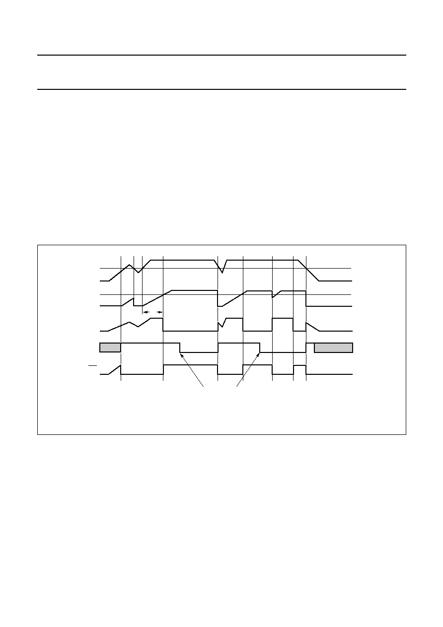
2003 Oct 30
43
Philips Semiconductors
Product specification
Low power single card reader
TDA8029
8.11
Supply
The circuit operates within a supply voltage range of
2.7 to 6 V. The supply pins are V
DD
, DCIN, GND and
PGND. Pins DCIN and PGND supply the analog drivers to
the cards and have to be externally decoupled because of
the large current spikes the card and the step-up converter
can create. V
DD
and GND supply the rest of the chip.
An integrated spike killer ensures the contacts to the card
to remain inactive during power-up or -down. An internal
voltage reference is generated which is used within the
step-up converter, the voltage supervisor, and the V
CC
generators.
V
DCIN
may be higher than V
DD
.
The voltage supervisor generates an alarm pulse, whose
length is defined by an external capacitor connected to the
CDEL pin, when V
DD
is too low to ensure proper operation
(1 ms per 2 nF typical). This pulse is used as a Power-on
reset pulse, and also to block either any spurious signals
on card contacts during controllers reset or to force an
automatic deactivation of the contacts in the event of
supply drop-out (see Sections 8.16 and 8.17).
After power-on or after a voltage drop, the bit SUPL is set
within the Hardware Status Register (HSR) and remains
set until HSR is read when the alarm pulse is inactive.
As long as the Power-on reset is active, INT0_N is LOW.
The same occurs when leaving shut-down mode or when
the RESET pin has been set active.
handbook, full pagewidth
Vth1
VDD
Vth2
CDEL
RSTOUT
SUPL
INT
Supply dropout
Power-off
Reset by CDEL
Power-on
Status read
MDB815
tw
Fig.11 Voltage supervisor.

2003 Oct 30
44
Philips Semiconductors
Product specification
Low power single card reader
TDA8029
8.12
DC/DC converter
Except for V
CC
generator, and the other card contacts
buffers, the whole circuit is powered by V
DD
and DCIN.
If the supply voltage is 2.7 V, then a higher voltage is
needed for the ISO contacts supply. When a card session
is requested by the controller, the sequencer first starts the
DC/DC converter, which is a switched capacitors type,
clocked by an internal oscillator at a frequency of
approximately 2.5 MHz.
There are several possible situations:
∑
V
DCIN
= 3 V and V
CC
= 3 V: In this case the DC/DC
converter is acting as a doubler with a regulation of
about 4.0 V
∑
V
DCIN
= 3 V and V
CC
= 5 V: In this case the DC/DC
converter is acting as a tripler with a regulation of about
5.5 V
∑
V
DCIN
= 5 V and V
CC
= 3 V: In this case, the DC/DC
converter is acting as a follower, V
DD
is applied on VUP
∑
V
DCIN
= 5 V and V
CC
= 5 V. In this case, the DC/DC
converter is acting as a doubler with a regulation of
about 5.5 V
∑
V
CC
= 1.8 V. In this case, whatever value of V
DCIN
, the
DC/DC converter is acting as a follower, V
DD
is applied
on VUP.
The switch between different modes of the DC/DC
converter is done by the TDA8029 at about V
DCIN
= 3.5 V.
The output voltage is fed to the V
CC
generator. V
CC
and
GNDC are used as a reference for all other card contacts.
8.13
ISO 7816 security
The correct sequence during activation and deactivation of
the card is ensured through a specific sequencer, clocked
by a division ratio of the internal oscillator.
Activation (bit START = 1 in register PCR) is only possible
if the card is present (pin PRES is HIGH) and if the supply
voltage is correct (supervisor not active).
The presence of the card is signalled to the controller by
the HSR.
Bit PR1 in register MSR is set if the card is present. Bit
PRL1 in register HSR is set if PR1 has toggled.
During a session, the sequencer performs an automatic
emergency deactivation on the card in the event of card
take-off, short-circuit, supply dropout or overheating. The
card is also automatically deactivated in case of supply
voltage drop or overheating. The HSR register is updated
and the INT0_N line falls down, so the system controller is
aware of what happened.
8.14
Protections and limitations
The TDA8029 features the following protections and
limitations:
∑
I
CC
limited to 100 mA, and deactivation when this limit is
reached
∑
Current to or from pin RST limited to 20 mA, and
deactivation when this limit is reached
∑
Deactivation when the temperature of the die exceeds
150
∞
C
∑
Current to or from pin I/O limited to 10 mA
∑
Current to or from pin CLK limited to 70 mA
∑
ESD protection on all cards contacts and pin PRES at
minimum 6 kV, thus no need of extra components for
protecting against ESD flash caused by a charged card
being introduced in the slot
∑
Short circuit between any card contacts can have any
duration without any damage.
8.15
Power reduction modes
On top of the standard controller power reduction features
described in the microcontroller section, the TDA8029 has
several power reduction modes that allow its use in
portable equipment, and help protecting the environment:
∑
Shut-down mode: when SDWN_N pin is LOW, then the
bit SDWN within HSR will be set, causing an interrupt on
INT0_N. The TDA8029 will read the status, deactivate
the card if it was active, set all ports to logic 1 and enter
Power-down mode by setting bit PD in the controller's
PCON register. In this mode, it will consume less than
20
µ
A, because the internal oscillator is stopped, and all
biasing currents are cut.
When SDWN_N returns to HIGH, a Power-on reset
operation is performed, so the chip is in the same state
than at power-on.
∑
Power-down mode: the microcontroller is in
Power-down mode, and the card is deactivated. The
bias currents in the chip and the frequency of the internal
oscillator are reduced. In this mode, the consumption is
less than 100
µ
A.
∑
Sleep mode: the microcontroller is in Power-down
mode, the card is activated, but with the clock stopped
HIGH or LOW. In this case, the card is supposed not to
draw more than 2 mA from V
CC
. The bias currents and
the frequency of the internal oscillator are also reduced.
With a current of 100
µ
A drawn by the card, the
consumption is less than 500
µ
A in tripler mode, 400
µ
A
in doubler mode, or 300
µ
A in follower mode.

2003 Oct 30
45
Philips Semiconductors
Product specification
Low power single card reader
TDA8029
When in Power-down or Sleep mode, card extraction or
insertion, overcurrent on V
CC
, or HIGH level on pins RST
or RESET will wake up the chip.
The same occurs in case of a falling edge on RX if bit
ENRX is set, or on INT1_N if bit ENINT1 is set and if
INT1_N is enabled within the controller.
If only INT1_N should wake up the TDA8029, then INT1_N
must be enabled in the controller, and ENINT1 only should
be set.
If RX should wake up the TDA8029, then INT1_N must be
enabled in the controller, and ENRX and ENINT1 should
be set.
In case of wake up by RX, then the first received
characters may be lost, depending on the baud rate on the
serial link. (The controller waits for 1536 clock cycles
before leaving Power-down mode).
For more details about the use of these modes, please
refer to the application notes
"AN00069" and "AN01005".
8.16
Activation sequence
When the card is inactive, V
CC
, CLK, RST and I/O are
LOW, with low impedance with respect to GNDC. The
DC/DC converter is stopped.
When everything is satisfactory (voltage supply, card
present and no hardware problems), the system controller
may initiate an activation sequence of the card. Figure 12
shows the activation sequence.
After leaving the UART reset mode, and then configuring
the necessary parameters for the UART, it may set the bit
START in register PCR (t
0
). The following sequence will
take place:
∑
The DC/DC converter is started (t
1
)
∑
V
CC
starts rising from 0 to 5 V or 3 V with a controlled
rise time of 0.17 V/
µ
s typically (t
2
)
∑
I/O rises to V
CC
(t
3
), (Integrated 14 k
pull-up to V
CC
)
∑
CLK is sent to the card and RST is enabled (t
4
).
After a number of clock pulses that can be counted with the
time out counter, bit RSTIN may be set by software, then
pin RST rises to V
CC
.
The sequencer is clocked by
1
/
64
f
int
which leads to a time
interval T of 25
µ
s typical. Thus t
1
= 0 to
3
/
64
T,
t
2
= t
1
+
3
/
2
T, t
3
= t
1
+
7
/
2
T, and t
4
= t
1
+ 4T.
handbook, full pagewidth
START
VUP
VCC
I/O
RSTIN
CLK
RST
t0
t2
t3
t4 = tact
ATR
t1
FCE684
Fig.12 Activation sequence.

2003 Oct 30
46
Philips Semiconductors
Product specification
Low power single card reader
TDA8029
8.17
Deactivation sequence
When the session is completed, the microcontroller resets
bit START (t
10
). The circuit then executes an automatic
deactivation sequence shown in Fig.13:
∑
Card reset (pin RST falls LOW) (t
11
)
∑
Clock (pin CLK) is stopped LOW (t
12
)
∑
Pin I/O falls to 0 V (t
13
)
∑
V
CC
falls to 0 V with typical 0.17 V/
µ
s slew rate (t
14
)
∑
The DC/DC converter is stopped and CLK, RST, V
CC
and I/O become low impedance to GNDC (t
15
).
t
11
= t
10
+
3
/
64
T, t
12
= t
11
+
1
/
2
T, t
13
= t
11
+ T,
t
14
= t
11
+
3
/
2
T, t
15
= t
11
+
7
/
2
T.
t
de
is the time that V
CC
needs for going down to less than
0.4 V.
Automatic emergency deactivation is performed in the
following cases:
∑
Withdrawal of the card (PRES LOW)
∑
Overcurrent detection on V
CC
(bit PRTL1 set)
∑
Overcurrent detection on RST (bit PRTL1 set)
∑
Overheating (bit PTL set)
∑
Supply too low (bit SUPL set)
∑
RESET pin active HIGH.
If the reason of the deactivation is a card take off, an
overcurrent or an overheating, then INT0_N is LOW. The
corresponding bit in the hardware status register is set. Bit
START is automatically reset.
If the reason is a supply dropout, then the deactivation
sequence occurs, and a complete reset of the chip is
performed. When the supply will be OK again, then the bit
SUPL will be set in HSR.
handbook, full pagewidth
START
VUP
VCC
I/O
CLK
RST
t10
t12
t13
tde
t14
t15
t11
FCE685
Fig.13 Deactivation sequence.

2003 Oct 30
47
Philips Semiconductors
Product specification
Low power single card reader
TDA8029
9
LIMITING VALUES
In accordance with the Absolute Maximum Rating System (IEC 60134).
Note
1. Human body model as defined in JEDEC Standard JESD22-A114-B, dated June 2000.
10 HANDLING
Inputs and outputs are protected against electrostatic discharge voltages during normal handling. However, to be totally
safe, it is desirable to take normal precautions appropriate to handling MOS devices.
11 THERMAL CHARACTERISTICS
SYMBOL
PARAMETER
CONDITIONS
MIN.
MAX.
UNIT
V
DCIN
input voltage for the DC/DC converter
-
0.5
+6.5
V
V
DD
supply voltage
-
0.5
+6.5
V
V
n
voltage limit
on pins SAM, SBM, SAP, SBP and VUP
-
0.5
7.5
V
on all other pins
-
0.5
V
DD
+ 0.5
V
P
tot
continuous total power dissipation
T
amb
=
-
40 to +90
∞
C
-
500
mW
T
stg
storage temperature
-
55
+150
∞
C
T
j
junction temperature
-
125
∞
C
V
esd
electrostatic discharge voltage
human body model;
note 1
on pins I/O, V
CC
, RST, CLK and GNDC
-
6
+6
kV
on pin PRES
-
3
+3
kV
on pins SAM and SBM
-
1
+1
kV
on other pins
-
2
+2
kV
SYMBOL
PARAMETER
CONDITIONS
VALUE
UNIT
R
th(j-a)
thermal resistance from junction to
ambient
in free air
80
K/W

2003 Oct 30
48
Philips Semiconductors
Product specification
Low power single card reader
TDA8029
12 CHARACTERISTICS
V
DD
= V
DCIN
= 3.3 V; T
amb
= 25
∞
C; unless otherwise specified.
SYMBOL
PARAMETER
CONDITIONS
MIN.
TYP.
MAX.
UNIT
Supply
V
DD
supply voltage
2.7
-
6.0
V
V
DCIN
input voltage for the
DC/DC converter
V
DD
-
6.0
V
I
DD(sd)
supply current in
shut-down mode
V
DD
= 3.3 V
-
-
20
µ
A
I
DD(pd)
supply current in
Power-down mode
V
DD
= 3.3 V; card inactive;
microcontroller in Power-down
mode
-
-
110
µ
A
I
DD(sl)
supply current in Sleep
mode
V
DD
= 3.3 V; card active at
V
CC
= 5 V; clock stopped;
microcontroller in Power-down
mode; I
CC
= 0
µ
A
-
-
675
µ
A
I
DD(om)
supply current in operating
mode
I
CC
= 65 mA; f
XTAL
= 20 MHz;
f
CLK
= 10 MHz; 5 V card;
V
DD
= 2.7 V
-
-
250
mA
I
CC
= 50 mA; f
XTAL
= 20 MHz;
f
CLK
= 10 MHz; 3 V card;
V
DD
= 2.7 V
-
-
125
mA
I
CC
= 50 mA; f
XTAL
= 20 MHz;
f
CLK
= 10 MHz; 3 V card;
V
DD
= 5 V
-
-
65
mA
V
th1
threshold voltage on V
DD
(falling)
2.15
-
2.45
V
V
hys1
hysteresis on V
th1
50
-
170
mV
V
th2
threshold voltage on pin
CDEL
-
1.25
-
V
V
CDEL
voltage on pin CDEL
-
-
V
DD
+ 0.3
V
I
CDEL
output current at pin CDEL charge: pin grounded
-
-
2
-
µ
A
discharge: V
CDEL
= V
DD
-
2
-
mA
C
CDEL
capacitance value
1
-
-
nF
t
W(alarm)
alarm pulse width
C
CDEL
= 22 nF
-
10
-
ms
Crystal oscillator: pins XTAL1 and XTAL2
f
XTAL
crystal frequency
V
DD
= 5 V
4
-
27
MHz
V
DD
< 3 V
4
-
16
MHz
f
ext
external frequency applied
on XTAL1
0
-
25
MHz
V
IH
HIGH level input voltage on
XTAL1
0.8V
DD
-
V
DD
+ 0.2
V
V
IL
LOW level input voltage on
XTAL1
-
0.3
-
0.2V
DD
V
2003 Oct 30
49
Philips Semiconductors
Product specification
Low power single card reader
TDA8029
DC/DC converter
f
int
oscillation frequency
2
2.6
3.2
MHz
V
VUP
voltage on pin VUP
5 V card
-
5.7
-
V
3 V card
-
4.1
-
V
V
det
detection voltage for
doubler/tripler selection
3.4
3.5
3.6
V
Reset output to the card: pin RST
V
O(inactive)
output voltage in inactive
mode
no load
0
-
0.1
V
I
O(inactive)
= 1 mA
0
-
0.3
V
I
O(inactive)
current from RST when
inactive and pin grounded
0
-
-
1
mA
V
OL
LOW level output voltage
I
OL
= 200
µ
A
0
-
0.3
V
V
OH
HIGH level output voltage
I
OH
=
-
200
µ
A
0.9V
CC
-
V
CC
V
t
r
rise time
C
L
= 250 pF
-
-
0.1
µ
s
t
f
fall time
C
L
= 250 pF
-
-
0.1
µ
s
Clock output to the card: pin CLK
V
O(inactive)
output voltage in inactive
mode
no load
0
-
0.1
V
I
O(inactive)
= 1 mA
0
-
0.3
V
I
O(inactive)
current from pin CLK
inactive and pin grounded
0
-
-
1
mA
V
OL
LOW level output voltage
I
OL
= 200
µ
A
0
-
0.3
V
V
OH
HIGH level output voltage
I
OH
=
-
200
µ
A
0.9V
CC
-
V
CC
V
t
r
rise time
C
L
= 35 pF, V
CC
= 5 or 3 V
-
-
10
ns
t
f
fall time
C
L
= 35 pF, V
CC
= 5 or 3 V
-
-
10
ns
f
clk
clock frequency
1 MHz idle configuration
1
-
1.5
MHz
operational
0
-
20
MHz
duty cycle
except for XTAL; C
L
= 35 pF
45
-
55
%
SR
r
, SR
f
slew rate, rise and fall
C
L
= 35 pF
0.2
-
-
V/ns
Card supply voltage: pin V
CC
; 2 ceramic multilayer capacitances with low ESR of minimum 100 nF should be
used in order to meet these specifications
V
O(inactive)
output voltage inactive
no load
0
-
0.1
V
I
O(inactive)
= 1 mA
0
-
0.3
V
I
O(inactive)
current from pin I/O
inactive and pin grounded
-
-
-
1
mA
SYMBOL
PARAMETER
CONDITIONS
MIN.
TYP.
MAX.
UNIT
2003 Oct 30
50
Philips Semiconductors
Product specification
Low power single card reader
TDA8029
V
CC
card supply voltage
active mode including static
loads; I
CC
< 65 mA; 5 V card
4.75
5.0
5.25
V
active mode; current pulses of
40 nAs with I < 200 mA,
t < 400 ns, f < 20 MHz;
5 V card
4.6
-
5.4
V
active mode including static
loads; I
CC
< 65 mA;
V
DD
> 3.0 V; 3 V card
2.78
3
3.22
V
active mode; current pulses of
24 nAs with I < 200 mA,
t < 400 ns, f < 20 MHz;
3 V card
2.75
-
3.25
V
active mode including static
loads; I
CC
< 30 mA; 1.8 V card
1.62
1.8
1.98
V
active mode; current pulses of
12 nAs with I < 200 mA,
t < 400 ns, f < 20 MHz;
1.8 V card
1.62
-
1.98
V
I
CC
card supply current
5 V card; V
CC
= 0 to 5 V
-
-
65
mA
3 V card; V
CC
= 0 to 3 V;
V
DD
> 3.0 V
-
-
65
mA
1.8 V card; V
CC
= 0 to 1.8 V
-
-
30
mA
V
CC
shorted to ground
-
-
120
mA
SR
r
, SR
f
rise and fall slew rate on
V
CC
maximum load capacitor
300 nF
0.05
0.16
0.22
V/
µ
s
V
ripple(p-p)
ripple voltage on V
CC
(peak to peak value)
20 kHz < f < 200 MHz
-
-
350
mV
Data line: pin I/O, with an integrated 14 k
pull-up resistor to V
CC
V
O(inactive)
output voltage inactive
no load
0
-
0.1
V
I
O(inactive)
= 1 mA
-
-
0.3
V
I
O(inactive)
current from I/O when
inactive and pin grounded
-
-
-
1
mA
V
OL
LOW level output voltage
I/O configured as output;
I
OL
= 1 mA
0
-
0.3
V
V
OH
HIGH level output voltage
I/O configured as output;
V
CC
= 5 or 3 V
I
OH
<
-
40
µ
A
0.75V
CC
-
V
CC
+ 0.25
V
I
OH
<
-
20
µ
A
0.8V
CC
-
V
CC
+ 0.25
V
V
IL
LOW level input voltage
I/O configured as input
-
0.3
-
0.8
V
V
IH
HIGH level input voltage
I/O configured as input
1.5
-
V
CC
V
I
IL
input current LOW
V
IL
= 0
-
-
500
µ
A
I
LI(H)
input leakage current
HIGH
V
IH
= V
CC
-
-
10
µ
A
SYMBOL
PARAMETER
CONDITIONS
MIN.
TYP.
MAX.
UNIT
2003 Oct 30
51
Philips Semiconductors
Product specification
Low power single card reader
TDA8029
t
i(r)
, t
i(f)
input rise and fall times
C
L
60 pF
-
-
1
µ
s
t
o(r)
, t
o(f)
output rise and fall times
C
L
60 pF
-
-
0.1
µ
s
R
pu
internal pull-up resistance
between I/O and V
CC
11
14
17
k
t
edge
width of active pull-up
pulse
I/O configured as output,
rising from LOW to HIGH
1
/
2
f
XTAL1
-
1
/
3
f
XTAL1
ns
I
edge
current from I/O when
active pull-up
V
OH
= 0.9 V
CC
; C = 60 pF
-
1
-
-
mA
Timings
t
act
activation sequence
duration
-
-
130
µ
s
t
de
deactivation sequence
duration
-
-
100
µ
s
Protections and limitations
I
CC(sd)
shut-down and limitation
current at V
CC
-
-
100
-
mA
I
I/O(lim)
limitation current on I/O
-
15
-
+15
mA
I
CLK(lim)
limitation current on CLK
-
70
-
+70
mA
I
RST(sd)
shut-down current on RST
-
-
20
-
mA
I
RST(lim)
limitation current on RST
-
20
-
+20
mA
T
sd
shut-down temperature
-
150
-
∞
C
Card presence input: pin PRES
V
IL
LOW level input voltage
-
-
0.3V
DD
V
V
IH
HIGH level input voltage
0.7V
DD
-
-
V
I
LI(L)
input leakage current LOW V
I
= 0
-
20
-
+20
µ
A
I
LI(H)
input leakage current
HIGH
V
I
= V
DD
-
20
-
+20
µ
A
Shut-down input: pin SDWN_N
V
IL
LOW level input voltage
-
-
0.3V
DD
V
V
IH
HIGH level input voltage
0.7V
DD
-
-
V
I
LI(L)
input leakage current LOW V
I
= 0
-
20
-
+20
µ
A
I
LI(H)
input leakage current
HIGH
V
I
= V
DD
-
20
-
+20
µ
A
General purpose I/O: pins P16, P17, P26, P27, INT1_N, RX and TX
V
IL
LOW level input voltage
-
-
0.2V
DD
V
V
IH
HIGH level input voltage
0.2V
DD
+ 0.9
-
-
V
V
OL
output voltage LOW
I
OL
= 1.6 mA
-
-
0.4
V
V
OH
output voltage HIGH
I
OH
=
-
30
µ
A
V
DD
-
0.7
-
-
V
I
IL
input current LOW
V
I
= 0.4 V
-
1
-
-
50
µ
A
I
THL
HIGH to LOW transition
current
V
I
= 2 V
-
-
-
650
µ
A
SYMBOL
PARAMETER
CONDITIONS
MIN.
TYP.
MAX.
UNIT

2003 Oct 30
52
Philips Semiconductors
Product specification
Low power single card reader
TDA8029
Reset input: pin RESET, active HIGH
V
IL
LOW level input voltage
-
-
0.2V
DD
V
V
IH
HIGH level input voltage
0.7V
DD
-
-
V
SYMBOL
PARAMETER
CONDITIONS
MIN.
TYP.
MAX.
UNIT
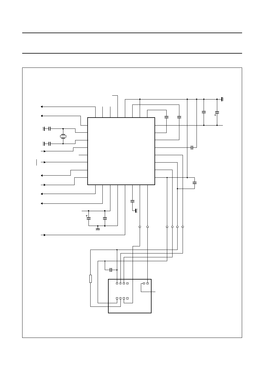
2003
Oct
30
53
Philips Semiconductors
Product specification
Lo
w po
w
er single card reader
TD
A8029
This text is here in white to force landscape pages to be rotated correctly when browsing through the pdf in the Acrobat reader.This text is here in
_
white to force landscape pages to be rotated correctly when browsing through the pdf in the Acrobat reader.This text is here inThis text is here in
white to force landscape pages to be rotated correctly when browsing through the pdf in the Acrobat reader. white to force landscape pages to be ...
13
APPLICA
TION INFORMA
TION
handbook, full pagewidth
10
µ
F
(16 V)
C9
C10
100 nF
C12
220 nF
C7
100 nF
C11
220 nF
220 nF
C8
C2
22 pF
C1
22 pF
14.745
MHz
Y1
TDA8029
FCE873
1
2
3
4
5
6
7
8
9
10
11
12
13
14
15
16
32
SHUTDOWN
P16
P17
RX
TX
INT1
RESET
P26
P27
31
30
29
28
27
26
25
24
23
22
21
20
19
18
17
R1
C3
100
nF
CARD READ UNIT
C5I
C6I
C7I
C8I
C1I
C2I
C3I
C4I
K1
K2
10
µ
F
(16 V)
100 nF
C5
22 nF
C6
C4
P17
P16
VDD
VDD
VDD
VDD
GND
SDWN_N
CDEL
I/O
PRES
P27
GNDC
CLK
V
CC
RST
GNDC
PRES
I/O
CLK
VCC
RST
VUP
SAP
SBP
DCIN
PSEN_N
ALE
EA_N
TEST
SAM
PGND
SBM
P26
XTAL1
XTAL2
RESET
P32/INT0_N
P33/INT1_N
P31/TX
P30/RX
VDCIN
Fig.13 Application diagram.
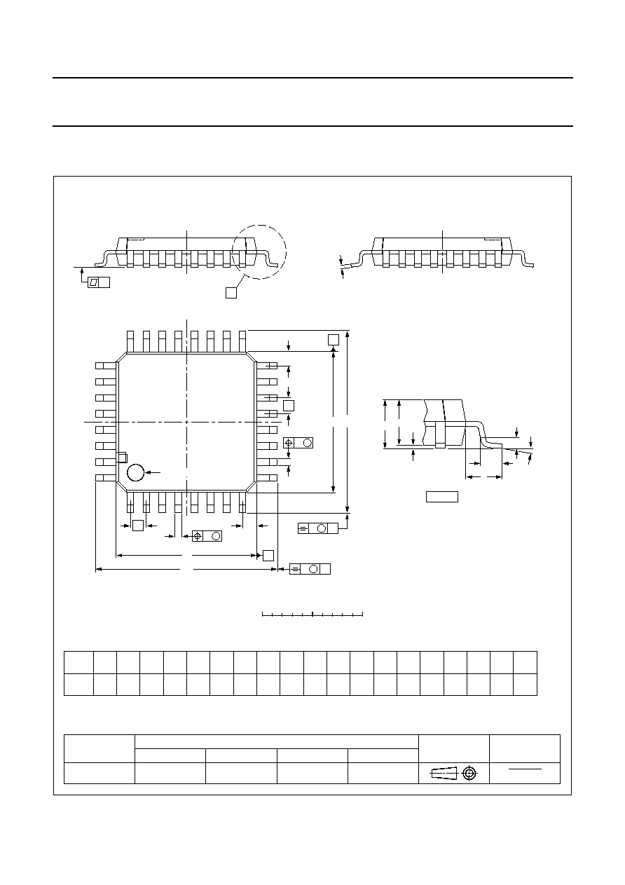
2003 Oct 30
54
Philips Semiconductors
Product specification
Low power single card reader
TDA8029
14 PACKAGE OUTLINE
UNIT
A
max.
A
1
A
2
A
3
b
p
c
E
(1)
e
H
E
L
L
p
Z
y
w
v
REFERENCES
OUTLINE
VERSION
EUROPEAN
PROJECTION
ISSUE DATE
IEC
JEDEC
JEITA
mm
1.6
0.20
0.05
1.45
1.35
0.25
0.4
0.3
0.18
0.12
7.1
6.9
0.8
9.15
8.85
0.9
0.5
7
0
o
o
0.25
0.1
1
0.2
DIMENSIONS (mm are the original dimensions)
Note
1. Plastic or metal protrusions of 0.25 mm maximum per side are not included.
0.75
0.45
SOT358 -1
136E03
MS-026
00-01-19
03-02-25
D
(1)
(1)
(1)
7.1
6.9
H
D
9.15
8.85
E
Z
0.9
0.5
D
b
p
e
E
A
1
A
L
p
detail X
L
(A )
3
B
8
c
D
H
b
p
E
H
A
2
v
M
B
D
Z D
A
Z E
e
v
M
A
X
1
32
25
24
17
16
9
y
pin 1 index
w
M
w
M
0
2.5
5 mm
scale
LQFP32: plastic low profile quad flat package; 32 leads; body 7 x 7 x 1.4 mm
SOT358-1

2003 Oct 30
55
Philips Semiconductors
Product specification
Low power single card reader
TDA8029
15 SOLDERING
15.1
Introduction to soldering surface mount
packages
This text gives a very brief insight to a complex technology.
A more in-depth account of soldering ICs can be found in
our
"Data Handbook IC26; Integrated Circuit Packages"
(document order number 9398 652 90011).
There is no soldering method that is ideal for all surface
mount IC packages. Wave soldering can still be used for
certain surface mount ICs, but it is not suitable for fine pitch
SMDs. In these situations reflow soldering is
recommended.
15.2
Reflow soldering
Reflow soldering requires solder paste (a suspension of
fine solder particles, flux and binding agent) to be applied
to the printed-circuit board by screen printing, stencilling or
pressure-syringe dispensing before package placement.
Driven by legislation and environmental forces the
worldwide use of lead-free solder pastes is increasing.
Several methods exist for reflowing; for example,
convection or convection/infrared heating in a conveyor
type oven. Throughput times (preheating, soldering and
cooling) vary between 100 and 200 seconds depending
on heating method.
Typical reflow peak temperatures range from
215 to 270
∞
C depending on solder paste material. The
top-surface temperature of the packages should
preferably be kept:
∑
below 220
∞
C (SnPb process) or below 245
∞
C (Pb-free
process)
≠ for all BGA and SSOP-T packages
≠ for packages with a thickness
2.5 mm
≠ for packages with a thickness < 2.5 mm and a
volume
350 mm
3
so called thick/large packages.
∑
below 235
∞
C (SnPb process) or below 260
∞
C (Pb-free
process) for packages with a thickness < 2.5 mm and a
volume < 350 mm
3
so called small/thin packages.
Moisture sensitivity precautions, as indicated on packing,
must be respected at all times.
15.3
Wave soldering
Conventional single wave soldering is not recommended
for surface mount devices (SMDs) or printed-circuit boards
with a high component density, as solder bridging and
non-wetting can present major problems.
To overcome these problems the double-wave soldering
method was specifically developed.
If wave soldering is used the following conditions must be
observed for optimal results:
∑
Use a double-wave soldering method comprising a
turbulent wave with high upward pressure followed by a
smooth laminar wave.
∑
For packages with leads on two sides and a pitch (e):
≠ larger than or equal to 1.27 mm, the footprint
longitudinal axis is preferred to be parallel to the
transport direction of the printed-circuit board;
≠ smaller than 1.27 mm, the footprint longitudinal axis
must be parallel to the transport direction of the
printed-circuit board.
The footprint must incorporate solder thieves at the
downstream end.
∑
For packages with leads on four sides, the footprint must
be placed at a 45
∞
angle to the transport direction of the
printed-circuit board. The footprint must incorporate
solder thieves downstream and at the side corners.
During placement and before soldering, the package must
be fixed with a droplet of adhesive. The adhesive can be
applied by screen printing, pin transfer or syringe
dispensing. The package can be soldered after the
adhesive is cured.
Typical dwell time of the leads in the wave ranges from
3 to 4 seconds at 250
∞
C or 265
∞
C, depending on solder
material applied, SnPb or Pb-free respectively.
A mildly-activated flux will eliminate the need for removal
of corrosive residues in most applications.
15.4
Manual soldering
Fix the component by first soldering two
diagonally-opposite end leads. Use a low voltage (24 V or
less) soldering iron applied to the flat part of the lead.
Contact time must be limited to 10 seconds at up to
300
∞
C.
When using a dedicated tool, all other leads can be
soldered in one operation within 2 to 5 seconds between
270 and 320
∞
C.

2003 Oct 30
56
Philips Semiconductors
Product specification
Low power single card reader
TDA8029
15.5
Suitability of surface mount IC packages for wave and reflow soldering methods
Notes
1. For more detailed information on the BGA packages refer to the
"(LF)BGA Application Note" (AN01026); order a copy
from your Philips Semiconductors sales office.
2. All surface mount (SMD) packages are moisture sensitive. Depending upon the moisture content, the maximum
temperature (with respect to time) and body size of the package, there is a risk that internal or external package
cracks may occur due to vaporization of the moisture in them (the so called popcorn effect). For details, refer to the
Drypack information in the
"Data Handbook IC26; Integrated Circuit Packages; Section: Packing Methods".
3. These transparent plastic packages are extremely sensitive to reflow soldering conditions and must on no account
be processed through more than one soldering cycle or subjected to infrared reflow soldering with peak temperature
exceeding 217
∞
C
±
10
∞
C measured in the atmosphere of the reflow oven. The package body peak temperature
must be kept as low as possible.
4. These packages are not suitable for wave soldering. On versions with the heatsink on the bottom side, the solder
cannot penetrate between the printed-circuit board and the heatsink. On versions with the heatsink on the top side,
the solder might be deposited on the heatsink surface.
5. If wave soldering is considered, then the package must be placed at a 45
∞
angle to the solder wave direction.
The package footprint must incorporate solder thieves downstream and at the side corners.
6. Wave soldering is suitable for LQFP, TQFP and QFP packages with a pitch (e) larger than 0.8 mm; it is definitely not
suitable for packages with a pitch (e) equal to or smaller than 0.65 mm.
7. Wave soldering is suitable for SSOP, TSSOP, VSO and VSSOP packages with a pitch (e) equal to or larger than
0.65 mm; it is definitely not suitable for packages with a pitch (e) equal to or smaller than 0.5 mm.
8. Hot bar or manual soldering is suitable for PMFP packages.
PACKAGE
(1)
SOLDERING METHOD
WAVE
REFLOW
(2)
BGA, LBGA, LFBGA, SQFP, SSOP-T
(3)
, TFBGA, VFBGA
not suitable
suitable
DHVQFN, HBCC, HBGA, HLQFP, HSQFP, HSOP, HTQFP,
HTSSOP, HVQFN, HVSON, SMS
not suitable
(4)
suitable
PLCC
(5)
, SO, SOJ
suitable
suitable
LQFP, QFP, TQFP
not recommended
(5)(6)
suitable
SSOP, TSSOP, VSO, VSSOP
not recommended
(7)
suitable
PMFP
(8)
not suitable
not suitable

2003 Oct 30
57
Philips Semiconductors
Product specification
Low power single card reader
TDA8029
16 DATA SHEET STATUS
Notes
1. Please consult the most recently issued data sheet before initiating or completing a design.
2. The product status of the device(s) described in this data sheet may have changed since this data sheet was
published. The latest information is available on the Internet at URL http://www.semiconductors.philips.com.
3. For data sheets describing multiple type numbers, the highest-level product status determines the data sheet status.
LEVEL
DATA SHEET
STATUS
(1)
PRODUCT
STATUS
(2)(3)
DEFINITION
I
Objective data
Development
This data sheet contains data from the objective specification for product
development. Philips Semiconductors reserves the right to change the
specification in any manner without notice.
II
Preliminary data Qualification
This data sheet contains data from the preliminary specification.
Supplementary data will be published at a later date. Philips
Semiconductors reserves the right to change the specification without
notice, in order to improve the design and supply the best possible
product.
III
Product data
Production
This data sheet contains data from the product specification. Philips
Semiconductors reserves the right to make changes at any time in order
to improve the design, manufacturing and supply. Relevant changes will
be communicated via a Customer Product/Process Change Notification
(CPCN).
17 DEFINITIONS
Short-form specification
The data in a short-form
specification is extracted from a full data sheet with the
same type number and title. For detailed information see
the relevant data sheet or data handbook.
Limiting values definition
Limiting values given are in
accordance with the Absolute Maximum Rating System
(IEC 60134). Stress above one or more of the limiting
values may cause permanent damage to the device.
These are stress ratings only and operation of the device
at these or at any other conditions above those given in the
Characteristics sections of the specification is not implied.
Exposure to limiting values for extended periods may
affect device reliability.
Application information
Applications that are
described herein for any of these products are for
illustrative purposes only. Philips Semiconductors make
no representation or warranty that such applications will be
suitable for the specified use without further testing or
modification.
18 DISCLAIMERS
Life support applications
These products are not
designed for use in life support appliances, devices, or
systems where malfunction of these products can
reasonably be expected to result in personal injury. Philips
Semiconductors customers using or selling these products
for use in such applications do so at their own risk and
agree to fully indemnify Philips Semiconductors for any
damages resulting from such application.
Right to make changes
Philips Semiconductors
reserves the right to make changes in the products -
including circuits, standard cells, and/or software -
described or contained herein in order to improve design
and/or performance. When the product is in full production
(status `Production'), relevant changes will be
communicated via a Customer Product/Process Change
Notification (CPCN). Philips Semiconductors assumes no
responsibility or liability for the use of any of these
products, conveys no licence or title under any patent,
copyright, or mask work right to these products, and
makes no representations or warranties that these
products are free from patent, copyright, or mask work
right infringement, unless otherwise specified.

© Koninklijke Philips Electronics N.V. 2003
SCA75
All rights are reserved. Reproduction in whole or in part is prohibited without the prior written consent of the copyright owner.
The information presented in this document does not form part of any quotation or contract, is believed to be accurate and reliable and may be changed
without notice. No liability will be accepted by the publisher for any consequence of its use. Publication thereof does not convey nor imply any license
under patent- or other industrial or intellectual property rights.
Philips Semiconductors ≠ a worldwide company
Contact information
For additional information please visit http://www.semiconductors.philips.com.
Fax: +31 40 27 24825
For sales offices addresses send e-mail to: sales.addresses@www.semiconductors.philips.com.
Printed in The Netherlands
R63/02/pp
58
Date of release:
2003 Oct 30
Document order number:
9397 750 11827