 | –≠–ª–µ–∫—Ç—Ä–æ–Ω–Ω—ã–π –∫–æ–º–ø–æ–Ω–µ–Ω—Ç: 80C552 | –°–∫–∞—á–∞—Ç—å:  PDF PDF  ZIP ZIP |
Document Outline
- DESCRIPTION
- FEATURES
- LOGIC SYMBOL
- PIN CONFIGURATIONS
- BLOCK DIAGRAM
- ORDERING INFORMATION
- PIN DESCRIPTION
- OSCILLATOR CHARACTERISTICS
- RESET
- IDLE MODE
- POWER-DOWN MODE
- ROM CODE PROTECTION (83C552)
- ABSOLUTE MAXIMUM RATINGS
- DEVICE SPECIFICATIONS
- DC ELECTRICAL CHARACTERISTICS
- DC ELECTRICAL CHARACTERISTICS (Continued)
- AC ELECTRICAL CHARACTERISTICS
- AC ELECTRICAL CHARACTERISTICS (Continued)
- AC ELECTRICAL CHARACTERISTICS (Continued)
- EXPLANATION OF THE AC SYMBOLS
- PACKAGE OUTLINE
- Data sheet status
- Definitions
- Disclaimers

Philips
Semiconductors
80C552/83C552
Single-chip 8-bit microcontroller
with
10-bit A/D, capture/compare timer,
high-speed outputs, PWM
Product data
Supersedes data of 1998 Aug 13
2002 Sep 03
INTEGRATED CIRCUITS

Philips Semiconductors
Product data
80C552/83C552
Single-chip 8-bit microcontroller with 10-bit A/D,
capture/compare timer, high-speed outputs, PWM
2
2002 Sep 03
853-1467 28849
DESCRIPTION
The 80C552/83C552 (hereafter generically referred to as 8XC552)
Single-Chip 8-Bit Microcontroller is manufactured in an advanced
CMOS process and is a derivative of the 80C51 microcontroller
family. The 8XC552 has the same instruction set as the 80C51.
Three versions of the derivative exist:
∑
83C552--8 kbytes mask programmable ROM
∑
80C552--ROMless version of the 83C552
∑
87C552--8 kbytes EPROM (described in a separate chapter)
The 8XC552 contains a non-volatile 8k
◊
8 read-only program
memory (83C552), a volatile 256
◊
8 read/write data memory, five
8-bit I/O ports, one 8-bit input port, two 16-bit timer/event counters
(identical to the timers of the 80C51), an additional 16-bit timer
coupled to capture and compare latches, a 15-source,
two-priority-level, nested interrupt structure, an 8-input ADC, a dual
DAC pulse width modulated interface, two serial interfaces (UART
and I
2
C-bus), a "watchdog" timer and on-chip oscillator and timing
circuits. For systems that require extra capability, the 8XC552 can
be expanded using standard TTL compatible memories and logic.
In addition, the 8XC552 has two software selectable modes of
power reduction--idle mode and power-down mode. The idle mode
freezes the CPU while allowing the RAM, timers, serial ports, and
interrupt system to continue functioning. The power-down mode
saves the RAM contents but freezes the oscillator, causing all other
chip functions to be inoperative.
The device also functions as an arithmetic processor having
facilities for both binary and BCD arithmetic plus bit-handling
capabilities. The instruction set consists of over 100 instructions: 49
one-byte, 45 two-byte, and 17 three-byte. With a 16 MHz (24 MHz)
crystal, 58% of the instructions are executed in 0.75
µ
s (0.5
µ
s) and
40% in 1.5
µ
s (1
µ
s). Multiply and divide instructions require 3
µ
s
(2
µ
s).
FEATURES
∑
80C51 central processing unit
∑
8k
◊
8 ROM expandable externally to 64 kbytes
∑
ROM code protection
∑
An additional 16-bit timer/counter coupled to four capture registers
and three compare registers
∑
Two standard 16-bit timer/counters
∑
256
◊
8 RAM, expandable externally to 64 kbytes
∑
Capable of producing eight synchronized, timed outputs
∑
A 10-bit ADC with eight multiplexed analog inputs
∑
Two 8-bit resolution, pulse width modulation outputs
∑
Five 8-bit I/O ports plus one 8-bit input port shared with analog
inputs
∑
I
2
C-bus serial I/O port with byte oriented master and slave
functions
∑
Full-duplex UART compatible with the standard 80C51
∑
On-chip watchdog timer
∑
Three speed ranges:
≠ 3.5 to 16 MHz
≠ 3.5 to 24 MHz (ROM, ROMless only)
∑
Three operating ambient temperature ranges:
≠ P83C552xBx: 0
∞
C to +70
∞
C
≠ P83C552xFx: ≠40
∞
C to +85
∞
C
(XTAL frequency max. 24 MHz)
≠ P83C552xHx: ≠40
∞
C to +125
∞
C
(XTAL frequency max. 16 MHz)
LOGIC SYMBOL
SU01691
POR
T
5
POR
T
4
ADC0-7
CMT0
CMT1
CMSR0-5
RST
EW
XTAL1
XTAL2
EA
ALE
PSEN
AVref+
AVref≠
STADC
PWM0
PWM1
POR
T
0
LOW ORDER
ADDRESS AND
DATA BUS
POR
T
1
POR
T
2
POR
T
3
CT0I
CT1I
CT2I
CT3I
T2
RT2
SCL
SDA
RxD/DATA
TxD/CLOCK
INT0
INT1
T0
T1
WR
RD
VSS
VDD
AVSS
AVDD
HIGH ORDER
ADDRESS AND
DATA BUS

Philips Semiconductors
Product data
80C552/83C552
Single-chip 8-bit microcontroller with 10-bit A/D,
capture/compare timer, high-speed outputs, PWM
2002 Sep 03
3
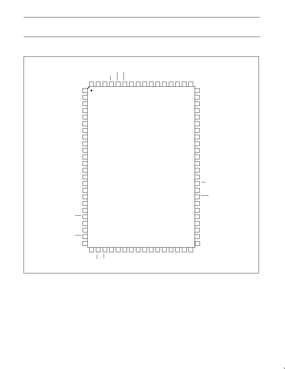
PIN CONFIGURATIONS
Plastic Leaded Chip Carrier
NC*
P3.7/RD
P3.6/WR
P5.0/ADC0
10
11
12
13
14
15
16
30
31
32
33
34
35
36
P4.3/CMSR3
P4.4/CMSR4
P4.5/CMSR5
P4.6/CMT0
P4.7/CMT1
P1.0/CT0I
RST
37
38
28
29
17
18
19
20
P1.1/CT1I
P1.2/CT2I
P1.4/T2
P1.3/CT3I
PLASTIC LEADED CHIP CARRIER
SU00932
21
22
23
24
25
26
P1.5/RT2
P1.6/SCL
P1.7/SDA
P3.0/RxD
P3.2/INT0
P3.1/TxD
39
40
41
42
43
P3.4/T0
P3.5/T1
NC*
NC*
XT
AL2
XT
AL1
V
SS
P2.1/A09
P2.2/A10
P2.3/A1
1
P2.4/A12
60
59
58
57
56
55
54
AV
SS
AV
REF+
AV
REF≠
P0.0/AD0
P0.1/AD1
P0.3/AD3
P0.2/AD2
53
52
51
50
P0.4/AD4
P0.5/AD5
P0.7/AD7
P0.6/AD6
49
48
47
46
45
44
EA
ALE
PSEN
P2.7/A15
P2.5/A13
P2.6/A14
44
7
6
5
4
3
2
1
68
67
9
8
66
65
64
63
62
P4.2/CMSR2
P4.1/CMSR1
P4.0/CMSR0
EW
PWM1
PWM0
ST
ADC
P5.1/ADC1
P5.2/ADC2
P5.3/ADC3
P5.4/ADC4
P5.5/ADC5
P5.6/ADC6
P5.7/ADC7
61
27
AV
DD
V
DD
P3.3/INT1
V
SS
P2.0/A08
* Do not connect.
Philips Semiconductors
Product data
80C552/83C552
Single-chip 8-bit microcontroller with 10-bit A/D,
capture/compare timer, high-speed outputs, PWM
2002 Sep 03
4
Plastic Quad Flat Pack
V
DD
1
2
3
4
5
6
7
27
28
29
30
31
32
33
P4.1/CMSR1
P4.2/CMSR2
NC*
P4.3/CMSR3
P4.4/CMSR4
P4.6/CMT0
P4.5/CMSR5
34
35
25
26
8
9
10
11
P4.7/CMT1
RST
P1.1/CT1I
P1.0/CT0I
PLASTIC QUAD FLAT PACK
SU00931
12
13
14
15
16
17
P1.2/CT2I
P1.3/CT3I
P1.4/T2
P1.5/RT2
P1.7/SDA
P1.6/SCL
18
19
20
21
P3.0/RxD
P3.1/TxD
NC*
P3.2/INT0
22
23
24
NC*
P3.3/INT1
PP3.4/T0
36
37
38
39
40
P3.5/T1
P3.6/WR
P3.7/RD
NC*
NC*
NC*
XT
AL2
XT
AL1
IC
V
SS
V
SS
V
SS
NC*
P2.0/A08
P2.1/A09
P2.2/A10
64
63
62
61
60
59
58
P5.7/ADC7
AV
DD
NC*
AV
SS
AV
REF+
P0.0/AD0
AV
REF≠
57
56
55
54
P0.1/AD1
P0.2/AD2
P0.4/AD4
P0.3/AD3
53
52
51
50
49
48
P0.5/AD5
P0.6/AD6
P0.7/AD7
EA
PSEN
ALE
47
46
45
44
P2.7/A15
P2.6/A14
NC*
P2.5/A13
43
42
41
NC*
P2.4/A12
P2.3/A11
78
77
76
75
74
73
72
71
70
80
79
69
68
67
66
65
P4.0/SMSR0
NC*
NC*
EW
PWM1
PWM0
ST
ADC
IC
P5.0/ADC0
P5.1/ADC1
P5.2/ADC2
P5.3/ADC3
P5.4/ADC4
P5.5/ADC5
P5.6/ADC6
* Do not connect.
IC = Internally connected (do not use).

Philips Semiconductors
Product data
80C552/83C552
Single-chip 8-bit microcontroller with 10-bit A/D,
capture/compare timer, high-speed outputs, PWM
2002 Sep 03
5
BLOCK DIAGRAM
SU01692
CPU
ADC
8-BIT INTERNAL BUS
16
P0
P1
P2
P3
TxD
RxD
P5
P4
CT0I-CT3I
T2
RT2
CMSR0-CMSR5
CMT0, CMT1
RST
EW
XTAL1
XTAL2
EA
ALE
PSEN
WR
RD
T0
T1
INT0
INT1
VDD
VSS
PWM0
PWM1
AV
SS
AV
DD
AV
REF
≠ +
STADC
ADC0-7 SDA
SCL
3
3
3
3
3
3
0
2
1
1
1
4
1
1
5
0
1
2
ALTERNATE FUNCTION OF PORT 0
3
4
5
AD0-7
A8-15
3
3
16
T0, T1
TWO 16-BIT
TIMER/EVENT
COUNTERS
PROGRAM
MEMORY
8k x 8 ROM
DATA
MEMORY
256 x 8 RAM
DUAL
PWM
SERIAL
I2C PORT
80C51 CORE
EXCLUDING
ROM/RAM
PARALLEL I/O
PORTS AND
EXTERNAL BUS
SERIAL
UART
PORT
8-BIT
PORT
FOUR
16-BIT
CAPTURE
LATCHES
T2
16-BIT
TIMER/
EVENT
COUNTERS
T2
16-BIT
COMPARA-
TORS
wITH
REGISTERS
COMPARA-
TOR
OUTPUT
SELECTION
T3
WATCHDOG
TIMER
ALTERNATE FUNCTION OF PORT 1
ALTERNATE FUNCTION OF PORT 2
ALTERNATE FUNCTION OF PORT 3
ALTERNATE FUNCTION OF PORT 4
ALTERNATE FUNCTION OF PORT 5

Philips Semiconductors
Product data
80C552/83C552
Single-chip 8-bit microcontroller with 10-bit A/D,
capture/compare timer, high-speed outputs, PWM
2002 Sep 03
6
ORDERING INFORMATION
PHILIPS
PART ORDER NUMBER
PART MARKING
DRAWING
NUMBER
TEMPERATURE (
∞
C)
AND PACKAGE
FREQ
(MHz)
ROMless
ROM
1
(
)
P80C552EBA
P83C552EBA/xxx
SOT188-2
0 to +70,
Plastic Leaded Chip Carrier
16
P80C552EBB
P83C552EBB/xxx
SOT318-2
0 to +70,
Plastic Quad Flat Pack
16
P80C552EFA
P83C552EFA/xxx
SOT188-2
≠40 to +85,
Plastic Leaded Chip Carrier
16
P80C552EFB
P83C552EFB/xxx
SOT318-2
≠40 to +85,
Plastic Quad Flat Pack
16
P80C552EHA
P83C552EHA/xxx
SOT188-2
≠40 to +125,
Plastic Leaded Chip Carrier
16
P80C552EHB
P83C552EHB/xxx
SOT318-2
≠40 to +125,
Plastic Quad Flat Pack
16
P80C552IBA
P83C552IBA/xxx
SOT188-2
0 to +70,
Plastic Leaded Chip Carrier
24
P80C552IBB
P83C552IBB/xxx
SOT318-2
0 to +70,
Plastic Quad Flat Pack
24
P80C552IFA
P83C552IFA/xxx
SOT188-2
≠40 to +85,
Plastic Leaded Chip Carrier
24
P80C552IFB
P83C552IFB/xxx
SOT318-2
≠40 to +85,
Plastic Quad Flat Pack
24
NOTE:
1. xxx denotes the ROM code number.
2. For EPROM device specification, refer to
87C552 datasheet.
Philips Semiconductors
Product data
80C552/83C552
Single-chip 8-bit microcontroller with 10-bit A/D,
capture/compare timer, high-speed outputs, PWM
2002 Sep 03
7
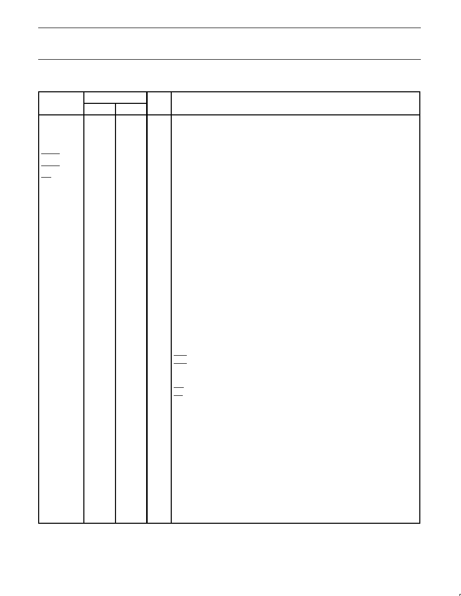
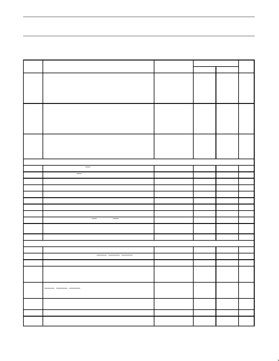
PIN DESCRIPTION
PIN NO.
MNEMONIC
PLCC
QFP
TYPE
NAME AND FUNCTION
V
DD
2
72
I
Digital Power Supply: +5 V power supply pin during normal operation, idle and
power-down mode.
STADC
3
74
I
Start ADC Operation: Input starting analog to digital conversion (ADC operation can also
be started by software). This pin must not float.
PWM0
4
75
O
Pulse Width Modulation: Output 0.
PWM1
5
76
O
Pulse Width Modulation: Output 1.
EW
6
77
I
Enable Watchdog Timer: Enable for T3 watchdog timer and disable power-down mode.
This pin must not float.
P0.0-P0.7
57-50
58-51
I/O
Port 0: Port 0 is an 8-bit open-drain bidirectional I/O port. Port 0 pins that have 1s written
to them float and can be used as high-impedance inputs. Port 0 is also the multiplexed
low-order address and data bus during accesses to external program and data memory. In
this application it uses strong internal pull-ups when emitting 1s.
P1.0-P1.7
16-23
10-17
I/O
Port 1: 8-bit I/O port. Alternate functions include:
16-21
10-15
I/O
(P1.0-P1.5): Quasi-bidirectional port pins.
22-23
16-17
I/O
(P1.6, P1.7): Open drain port pins.
16-19
10-13
I
CT0I-CT3I (P1.0-P1.3): Capture timer input signals for timer T2.
20
14
I
T2 (P1.4): T2 event input.
21
15
I
RT2 (P1.5): T2 timer reset signal. Rising edge triggered.
22
16
I/O
SCL (P1.6): Serial port clock line I
2
C-bus.
23
17
I/O
SDA (P1.7): Serial port data line I
2
C-bus.
Port 1 is also used to input the lower order address byte during EPROM programming and
verification. A0 is on P1.0, etc.
P2.0-P2.7
39-46
38-42,
45-47
I/O
Port 2: 8-bit quasi-bidirectional I/O port.
Alternate function: High-order address byte for external memory (A08-A15).
P3.0-P3.7
24-31
18-20,
23-27
I/O
Port 3: 8-bit quasi-bidirectional I/O port. Alternate functions include:
24
18
RxD(P3.0): Serial input port.
25
19
TxD (P3.1): Serial output port.
26
20
INT0 (P3.2): External interrupt.
27
23
INT1 (P3.3): External interrupt.
28
24
T0 (P3.4): Timer 0 external input.
29
25
T1 (P3.5): Timer 1 external input.
30
26
WR (P3.6): External data memory write strobe.
31
27
RD (P3.7): External data memory read strobe.
P4.0-P4.7
7-14
80, 1-2
4-8
I/O
Port 4: 8-bit quasi-bidirectional I/O port. Alternate functions include:
7-12
80, 1-2
4-6
O
CMSR0-CMSR5 (P4.0-P4.5): Timer T2 compare and set/reset outputs on a match with
timer T2.
13, 14
7, 8
O
CMT0, CMT1 (P4.6, P4.7): Timer T2 compare and toggle outputs on a match with timer T2.
P5.0-P5.7
68-62,
71-64,
I
Port 5: 8-bit input port.
1
ADC0-ADC7 (P5.0-P5.7): Alternate function: Eight input channels to ADC.
RST
15
9
I/O
Reset: Input to reset the 8XC552. It also provides a reset pulse as output when timer T3
overflows.
XTAL1
35
32
I
Crystal Input 1: Input to the inverting amplifier that forms the oscillator, and input to the
internal clock generator. Receives the external clock signal when an external oscillator is
used.
XTAL2
34
31
O
Crystal Input 2: Output of the inverting amplifier that forms the oscillator. Left open-circuit
when an external clock is used.
Philips Semiconductors
Product data
80C552/83C552
Single-chip 8-bit microcontroller with 10-bit A/D,
capture/compare timer, high-speed outputs, PWM
2002 Sep 03
8
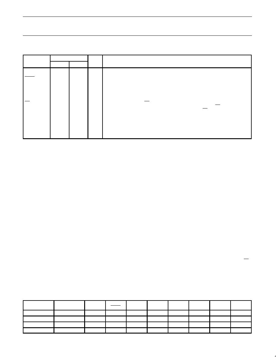
PIN DESCRIPTION (Continued)
PIN NO.
MNEMONIC
PLCC
QFP
TYPE
NAME AND FUNCTION
V
SS
36, 37
34-36
I
Two Digital ground pins.
PSEN
47
48
O
Program Store Enable: Active-low read strobe to external program memory.
ALE
48
49
O
Address Latch Enable: Latches the low byte of the address during accesses to external
memory. It is activated every six oscillator periods. During an external data memory
access, one ALE pulse is skipped. ALE can drive up to eight LS TTL inputs and handles
CMOS inputs without an external pull-up.
EA
49
50
I
External Access: When EA is held at TTL level high, the CPU executes out of the internal
program ROM provided the program counter is less than 8192. When EA is held at TTL
low level, the CPU executes out of external program memory. EA is not allowed to float.
AV
REF≠
58
59
I
Analog to Digital Conversion Reference Resistor: Low-end.
AV
REF+
59
60
I
Analog to Digital Conversion Reference Resistor: High-end.
AV
SS
60
61
I
Analog Ground
AV
DD
61
63
I
Analog Power Supply
NOTE:
1. To avoid "latch-up" effect at power-on, the voltage on any pin at any time must not be higher or lower than V
DD
+ 0.5 V or V
SS
≠ 0.5 V,
respectively.
OSCILLATOR CHARACTERISTICS
XTAL1 and XTAL2 are the input and output, respectively, of an
inverting amplifier. The pins can be configured for use as an on-chip
oscillator, as shown in the logic symbol, page 2.
To drive the device from an external clock source, XTAL1 should be
driven while XTAL2 is left unconnected. There are no requirements
on the duty cycle of the external clock signal, because the input to
the internal clock circuitry is through a divide-by-two flip-flop.
However, minimum and maximum high and low times specified in
the data sheet must be observed.
RESET
A reset is accomplished by holding the RST pin high for at least two
machine cycles (24 oscillator periods), while the oscillator is running.
To insure a good power-on reset, the RST pin must be high long
enough to allow the oscillator time to start up (normally a few
milliseconds) plus two machine cycles. At power-on, the voltage on
V
DD
and RST must come up at the same time for a proper start-up.
IDLE MODE
In the idle mode, the CPU puts itself to sleep while some of the
on-chip peripherals stay active. The instruction to invoke the idle
mode is the last instruction executed in the normal operating mode
before the idle mode is activated. The CPU contents, the on-chip
RAM, and all of the special function registers remain intact during
this mode. The idle mode can be terminated either by any enabled
interrupt (at which time the process is picked up at the interrupt
service routine and continued), or by a hardware reset which starts
the processor in the same manner as a power-on reset.
POWER-DOWN MODE
In the power-down mode, the oscillator is stopped and the
instruction to invoke power-down is the last instruction executed.
Only the contents of the on-chip RAM are preserved. A hardware
reset is the only way to terminate the power-down mode. The control
bits for the reduced power modes are in the special function register
PCON. Table 1 shows the state of the I/O ports during low current
operating modes.
ROM CODE PROTECTION (83C552)
The 83C552 has an additional security feature. ROM code
protection may be selected by setting a mask≠programmable
security bit (i.e., user dependent). This feature may be requested
during ROM code submission. When selected, the ROM code is
protected and cannot be read out at any time by any test mode or by
any instruction in the external program memory space.
The MOVC instructions are the only instructions that have access to
program code in the internal or external program memory. The EA
input is latched during RESET and is "don't care" after RESET
(also if the security bit is not set). This implementation prevents
reading internal program code by switching from external program
memory to internal program memory during a MOVC instruction or
any other instruction that uses immediate data.
Table 1. External Pin Status During Idle and Power-Down Modes
MODE
PROGRAM
MEMORY
ALE
PSEN
PORT 0
PORT 1
PORT 2
PORT 3
PORT 4
PWM0/
PWM1
Idle
Internal
1
1
Data
Data
Data
Data
Data
1
Idle
External
1
1
Float
Data
Address
Data
Data
1
Power-down
Internal
0
0
Data
Data
Data
Data
Data
1
Power-down
External
0
0
Float
Data
Data
Data
Data
1
Philips Semiconductors
Product data
80C552/83C552
Single-chip 8-bit microcontroller with 10-bit A/D,
capture/compare timer, high-speed outputs, PWM
2002 Sep 03
9
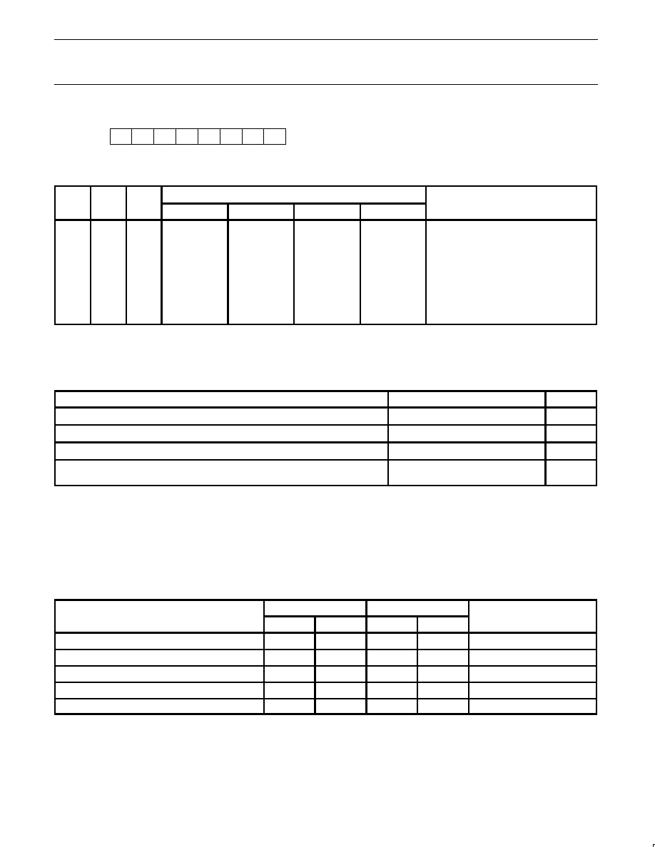
Serial Control Register (S1CON) ≠ See Table 2
CR2
ENS1
STA
STO
SI
AA
CR1
CR0
S1CON (D8H)
Bits CR0, CR1 and CR2 determine the serial clock frequency that is generated in the master mode of operation.
Table 2. Serial Clock Rates
BIT FREQUENCY (kHz) AT f
OSC
CR2
CR1
CR0
6 MHZ
12 MHz
16 MHz
24 MHz
2
f
OSC
DIVIDED BY
0
0
0
23
47
62.5
94
256
0
0
1
27
54
71
107
1
224
0
1
0
31
63
83.3
125
1
192
0
1
1
37
75
100
150
1
160
1
0
0
6.25
12.5
17
25
960
1
0
1
50
100
133
1
200
1
120
1
1
0
100
200
267
1
400
1
60
1
1
1
0.24 < 62.5
0.49 < 62.5
0.65 < 55.6
0.98 < 50.0
96
◊
(256 ≠ (reload value Timer 1))
0 < 255
0 < 254
0 < 253
0 <251
reload value Timer 1 in Mode 2.
NOTES:
1. These frequencies exceed the upper limit of 100kHz of the I
2
C-bus specification and cannot be used in an I
2
C-bus application.
2. At f
OSC
= 24 MHz the maximum I
2
C bus rate of 100kHz cannot be realized due to the fixed divider rates.
ABSOLUTE MAXIMUM RATINGS
1, 2, 3
PARAMETER
RATING
UNIT
Storage temperature range
≠65 to +150
∞
C
Voltage on any other pin to V
SS
≠0.5 to +6.5
V
Input, output DC current on any single I/O pin
5.0
mA
Power dissipation
(based on package heat transfer limitations, not device power consumption)
1.0
W
NOTES:
1. Stresses above those listed under Absolute Maximum Ratings may cause permanent damage to the device. This is a stress rating only and
functional operation of the device at these or any conditions other than those described in the AC and DC Electrical Characteristics section
of this specification is not implied.
2. This product includes circuitry specifically designed for the protection of its internal devices from the damaging effects of excessive static
charge. Nonetheless, it is suggested that conventional precautions be taken to avoid applying greater than the rated maxima.
3. Parameters are valid over operating temperature range unless otherwise specified. All voltages are with respect to V
SS
unless otherwise
noted.
DEVICE SPECIFICATIONS
SUPPLY VOLTAGE (V)
FREQUENCY (MHz)
TYPE
MIN
MAX
MIN
MAX
TEMPERATURE RANGE (
∞
C)
P83(0)C552EBx
4.5
5.5
3.5
16
0 to +70
P83(0)C552EFx
4.5
5.5
3.5
16
≠40 to +85
P83(0)C552EHx
4.5
5.5
3.5
16
≠40 to +125
P83(0)C552IBx
4.5
5.5
3.5
24
0 to +70
P83(0)C552IFx
4.5
5.5
3.5
24
≠40 to +85
Philips Semiconductors
Product data
80C552/83C552
Single-chip 8-bit microcontroller with 10-bit A/D,
capture/compare timer, high-speed outputs, PWM
2002 Sep 03
10
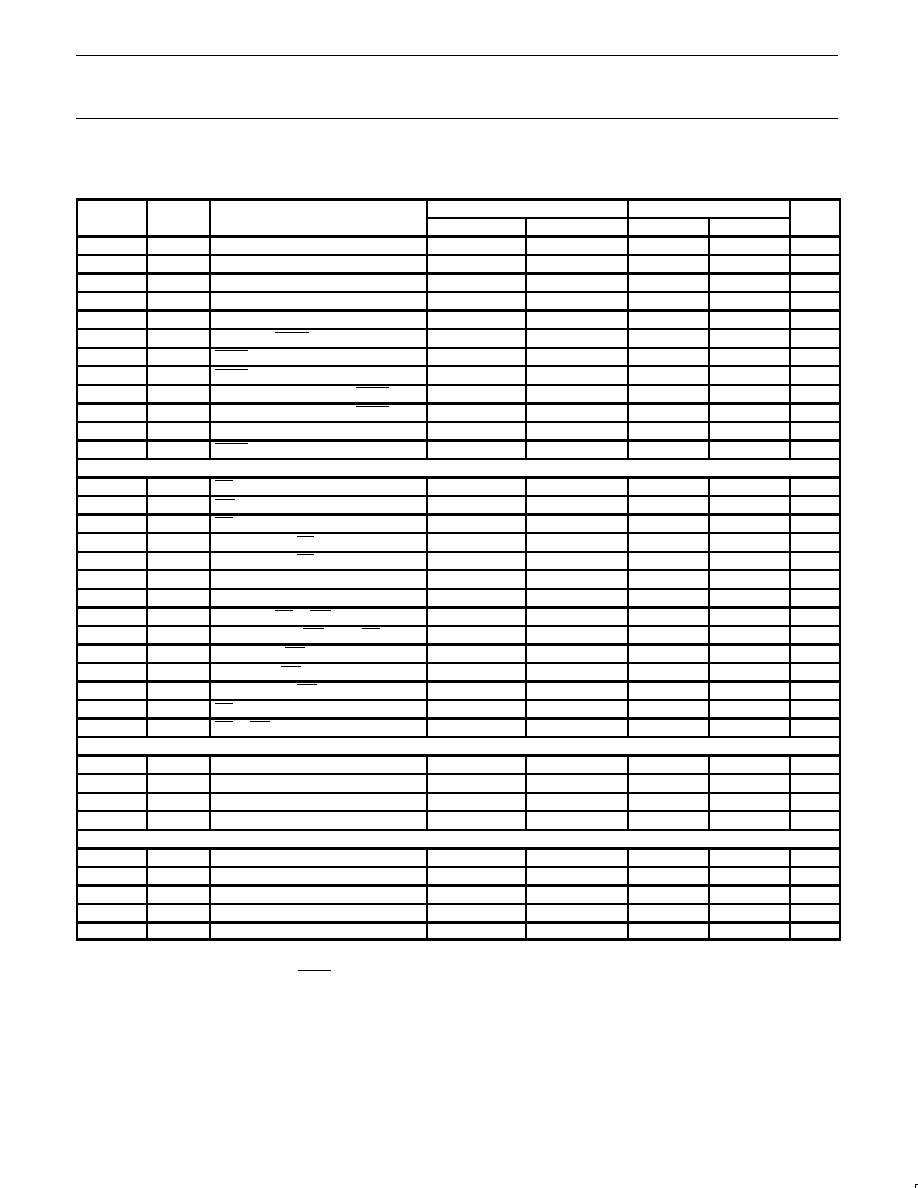
DC ELECTRICAL CHARACTERISTICS
V
SS
, AV
SS
= 0 V; V
DD
, AV
DD
= 5 V
±
10%
TEST
LIMITS
SYMBOL
PARAMETER
CONDITIONS
MIN
MAX
UNIT
I
DD
Supply current operating:
See notes 1 and 2
P83(0)C552EBx
f
OSC
= 16 MHz
45
mA
P83(0)C552EFx
f
OSC
= 16 MHz
45
mA
P83(0)C552EHx
f
OSC
= 16 MHz
40
mA
P83(0)C552IBx
f
OSC
= 24 MHz
55
mA
P83(0)C552IFx
f
OSC
= 24 MHz
55
mA
I
ID
Idle mode:
See notes 1 and 3
P83(0)C552EBx
f
OSC
= 16 MHz
10
mA
P83(0)C552EFx
f
OSC
= 16 MHz
10
mA
P83(0)C552EHx
f
OSC
= 16 MHz
9
mA
P83(0)C552IBx
f
OSC
= 24 MHz
12.5
mA
P83(0)C552IFx
f
OSC
= 24 MHz
12.5
mA
I
PD
Power-down current:
See notes 1 and 4;
2 V < V
PD
< V
DD
max
P83(0)C552xBx
50
µ
A
P83(0)C552xFx
50
µ
A
P83(0)C552xHx
150
µ
A
Inputs
V
IL
Input low voltage, except EA, P1.6, P1.7
≠0.5
0.2V
DD
≠0.1
V
V
IL1
Input low voltage to EA
≠0.5
0.2V
DD
≠0.3
V
V
IL2
Input low voltage to P1.6/SCL, P1.7/SDA
5
≠0.5
0.3V
DD
V
V
IH
Input high voltage, except XTAL1, RST, P1.6/SCL, P1.7/SDA
0.2V
DD
+0.9
V
DD
+0.5
V
V
IH1
Input high voltage, XTAL1, RST
0.7V
DD
V
DD
+0.5
V
V
IH2
Input high voltage, P1.6/SCL, P1.7/SDA
5
0.7V
DD
6.0
V
I
IL
Logical 0 input current, ports 1, 2, 3, 4, except P1.6, P1.7
V
IN
= 0.45 V
≠50
µ
A
I
TL
Logical 1-to-0 transition current, ports 1, 2, 3, 4, except P1.6, P1.7
See note 6
≠650
µ
A
±
I
IL1
Input leakage current, port 0, EA, STADC, EW
0.45 V < V
I
< V
DD
10
µ
A
±
I
IL2
Input leakage current, P1.6/SCL, P1.7/SDA
0 V < V
I
< 6 V
0 V < V
DD
< 5.5 V
10
µ
A
±
I
IL3
Input leakage current, port 5
0.45 V < V
I
< V
DD
1
µ
A
Outputs
V
OL
Output low voltage, ports 1, 2, 3, 4, except P1.6, P1.7
I
OL
= 1.6mA
7
0.45
V
V
OL1
Output low voltage, port 0, ALE, PSEN, PWM0, PWM1
I
OL
= 3.2mA
7
0.45
V
V
OL2
Output low voltage, P1.6/SCL, P1.7/SDA
I
OL
= 3.0mA
7
0.4
V
V
OH
Output high voltage, ports 1, 2, 3, 4, except P1.6/SCL, P1.7/SDA
≠I
OH
= 60
µ
A
2.4
V
≠I
OH
= 25
µ
A
0.75V
DD
V
≠I
OH
= 10
µ
A
0.9V
DD
V
V
OH1
Output high voltage (port 0 in external bus mode, ALE,
PSEN PWM0 PWM1)
8
≠I
OH
= 400
µ
A
2.4
V
PSEN, PWM0, PWM1)
8
≠I
OH
= 150
µ
A
0.75V
DD
V
≠I
OH
= 40
µ
A
0.9V
DD
V
V
OH2
Output high voltage (RST)
≠I
OH
= 400
µ
A
2.4
V
≠I
OH
= 120
µ
A
0.8V
DD
V
R
RST
Internal reset pull-down resistor
50
150
k
C
IO
Pin capacitance
Test freq = 1 MHz,
T
amb
= 25
∞
C
10
pF
Philips Semiconductors
Product data
80C552/83C552
Single-chip 8-bit microcontroller with 10-bit A/D,
capture/compare timer, high-speed outputs, PWM
2002 Sep 03
11
DC ELECTRICAL CHARACTERISTICS (Continued)
TEST
LIMITS
SYMBOL
PARAMETER
CONDITIONS
MIN
MAX
UNIT
Analog Inputs
AI
DD
Analog supply current: operating: (16 MHz)
Port 5 = 0 to AV
DD
1.2
mA
Analog supply current: operating: (24 MHz)
Port 5 = 0 to AV
DD
1.0
mA
AI
ID
Idle mode:
P83(0)C552EBx
50
µ
A
P83(0)C552EFx
50
µ
A
P83(0)C552EHx
100
µ
A
P83(0)C552IBx
50
µ
A
P83(0)C552IFx
50
µ
A
AI
PD
Power-down mode:
2 V < AV
PD
< AV
DD
max
P83(0)C552xBx
50
µ
A
P83(0)C552xFx
50
µ
A
P83(0)C552xHx
100
µ
A
AV
IN
Analog input voltage
AV
SS
≠0.2
AV
DD
+0.2
V
AV
REF
Reference voltage:
AV
REF≠
AV
SS
≠0.2
V
AV
REF+
AV
DD
+0.2
V
R
REF
Resistance between AV
REF+
and AV
REF≠
10
50
k
C
IA
Analog input capacitance
15
pF
t
ADS
Sampling time
8t
CY
µ
s
t
ADC
Conversion time (including sampling time)
50t
CY
µ
s
DL
e
Differential non-linearity
10, 11, 12
±
1
LSB
IL
e
Integral non-linearity
10, 13
±
2
LSB
OS
e
Offset error
10, 14
±
2
LSB
G
e
Gain error
10, 15
±
0.4
%
A
e
Absolute voltage error
10, 16
±
3
LSB
M
CTC
Channel to channel matching
±
1
LSB
C
t
Crosstalk
between inputs of port 5
17
0≠100kHz
≠60
dB
NOTES FOR DC ELECTRICAL CHARACTERISTICS:
1. See Figures 10 through 15 for I
DD
test conditions.
2. The operating supply current is measured with all output pins disconnected; XTAL1 driven with t
r
= t
f
= 10 ns; V
IL
= V
SS
+ 0.5 V;
V
IH
= V
DD
≠ 0.5 V; XTAL2 not connected; EA = RST = Port 0 = EW = V
DD
; STADC = V
SS
.
3. The idle mode supply current is measured with all output pins disconnected; XTAL1 driven with t
r
= t
f
= 10 ns; V
IL
= V
SS
+ 0.5 V;
V
IH
= V
DD
≠ 0.5 V; XTAL2 not connected; Port 0 = EW = V
DD
; EA = RST = STADC = V
SS
.
4. The power-down current is measured with all output pins disconnected; XTAL2 not connected; Port 0 = EW = V
DD
;
EA = RST = STADC = XTAL1 = V
SS
.
5. The input threshold voltage of P1.6 and P1.7 (SIO1) meets the I
2
C specification, so an input voltage below 1.5 V will be recognized as a
logic 0 while an input voltage above 3.0 V will be recognized as a logic 1.
6. Pins of ports 1 (except P1.6, P1.7), 2, 3, and 4 source a transition current when they are being externally driven from 1 to 0. The transition
current reaches its maximum value when V
IN
is approximately 2 V.
7. Capacitive loading on ports 0 and 2 may cause spurious noise to be superimposed on the V
OL
s of ALE and ports 1 and 3. The noise is due
to external bus capacitance discharging into the port 0 and port 2 pins when these pins make 1-to-0 transitions during bus operations. In the
worst cases (capacitive loading > 100 pF), the noise pulse on the ALE pin may exceed 0.8 V. In such cases, it may be desirable to qualify
ALE with a Schmitt Trigger, or use an address latch with a Schmitt Trigger STROBE input. I
OL
can exceed these conditions provided that no
single output sinks more than 5mA and no more than two outputs exceed the test conditions.
8. Capacitive loading on ports 0 and 2 may cause the V
OH
on ALE and PSEN to momentarily fall below the 0.9 V
DD
specification when the
address bits are stabilizing.
9. The following condition must not be exceeded: V
DD
≠ 0.2 V < AV
DD
< V
DD
+ 0.2 V.
10. Conditions: AV
REF≠
= 0 V; AV
DD
= 5.0 V, AV
REF+
(80C552, 83C552) = 5.12 V. ADC is monotonic with no missing codes. Measurement by
continuous conversion of AV
IN
= ≠20 mV to 5.12 V in steps of 0.5 mV.
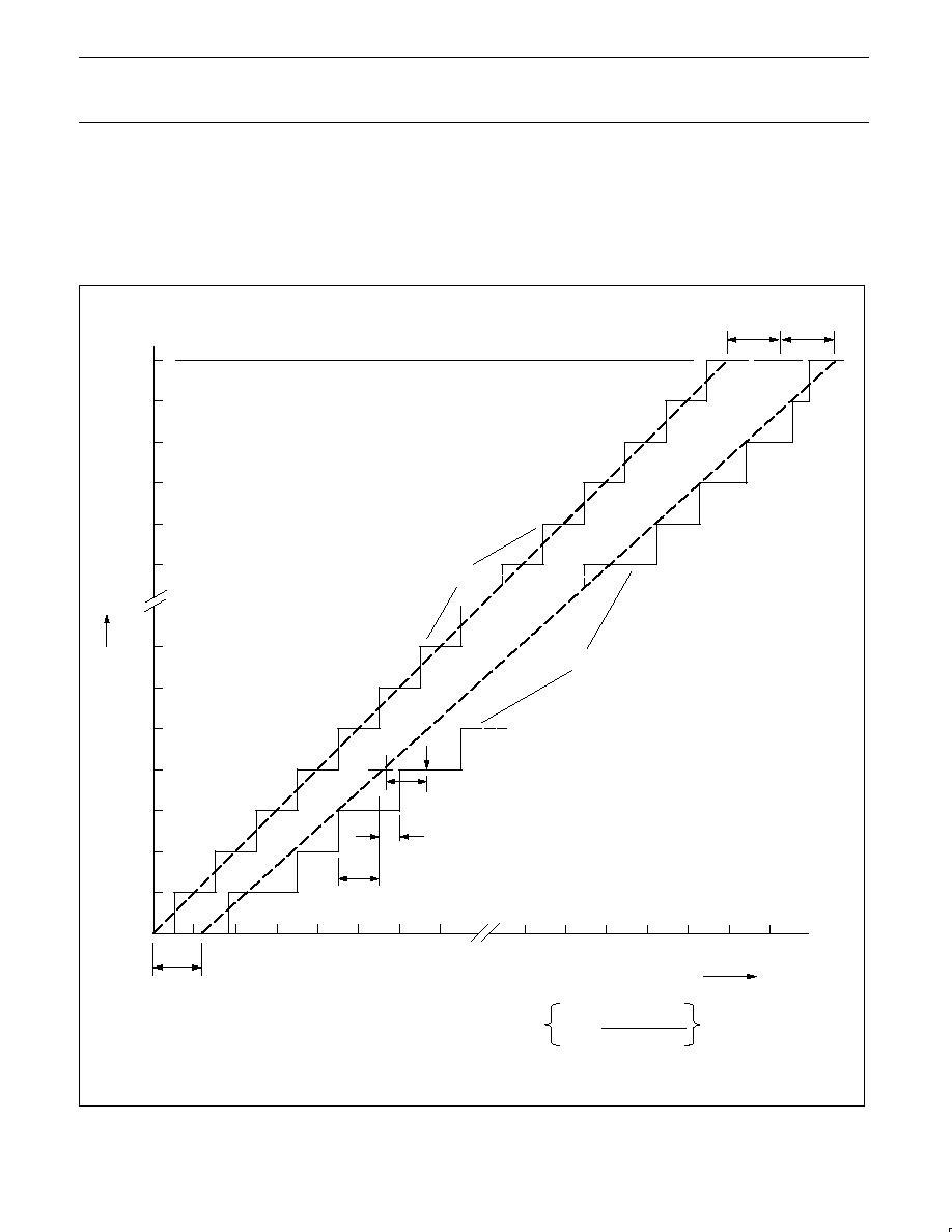
11. The differential non-linearity (DL
e
) is the difference between the actual step width and the ideal step width. (See Figure 1.)
12. The ADC is monotonic; there are no missing codes.
13. The integral non-linearity (IL
e
) is the peak difference between the center of the steps of the actual and the ideal transfer curve after
appropriate adjustment of gain and offset error. (See Figure 1.)
Philips Semiconductors
Product data
80C552/83C552
Single-chip 8-bit microcontroller with 10-bit A/D,
capture/compare timer, high-speed outputs, PWM
2002 Sep 03
12
14. The offset error (OS
e
) is the absolute difference between the straight line which fits the actual transfer curve (after removing gain error), and
a straight line which fits the ideal transfer curve. (See Figure 1.)
15. The gain error (G
e
) is the relative difference in percent between the straight line fitting the actual transfer curve (after removing offset error),
and the straight line which fits the ideal transfer curve. Gain error is constant at every point on the transfer curve. (See Figure 1.)
16. The absolute voltage error (A
e
) is the maximum difference between the center of the steps of the actual transfer curve of the non-calibrated
ADC and the ideal transfer curve.
17. This should be considered when both analog and digital signals are simultaneously input to port 5.
SU01693
1
0
2
3
4
5
6
7
1018
1019
1020
1021
1022
1023
1
2
3
4
5
6
7
1018
1019
1020
1021
1022
1023
1024
Code
Out
(2)
(1)
(5)
(4)
(3)
1 LSB
(ideal)
Offset
error
OSe
Offset
error
OSe
Gain
error
Ge
AVIN (LSBideal)
1 LSB =
AVREF+
≠
AVREF≠
1024
(1)
Example of an actual transfer curve.
(2)
The ideal transfer curve.
(3)
Differential non-linearity (DLe).
(4)
Integral non-linearity (ILe).
(5)
Center of a step of the actual transfer curve.
Figure 1. ADC Conversion Characteristic
Philips Semiconductors
Product data
80C552/83C552
Single-chip 8-bit microcontroller with 10-bit A/D,
capture/compare timer, high-speed outputs, PWM
2002 Sep 03
13
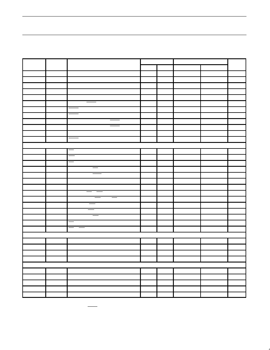
AC ELECTRICAL CHARACTERISTICS
1, 2
16 MHz version
16 MHz CLOCK
VARIABLE CLOCK
SYMBOL
FIGURE
PARAMETER
MIN
MAX
MIN
MAX
UNIT
1/t
CLCL
2
Oscillator frequency
3.5
16
MHz
t
LHLL
2
ALE pulse width
85
2t
CLCL
≠40
ns
t
AVLL
2
Address valid to ALE low
8
t
CLCL
≠55
ns
t
LLAX
2
Address hold after ALE low
28
t
CLCL
≠35
ns
t
LLIV
2
ALE low to valid instruction in
150
4t
CLCL
≠100
ns
t
LLPL
2
ALE low to PSEN low
23
t
CLCL
≠40
ns
t
PLPH
2
PSEN pulse width
143
3t
CLCL
≠45
ns
t
PLIV
2
PSEN low to valid instruction in
83
3t
CLCL
≠105
ns
t
PXIX
2
Input instruction hold after PSEN
0
0
ns
t
PXIZ
2
Input instruction float after PSEN
38
t
CLCL
≠25
ns
t
AVIV
2
Address to valid instruction in
208
5t
CLCL
≠105
ns
t
PLAZ
2
PSEN low to address float
10
10
ns
Data Memory
t
RLRH
3
RD pulse width
275
6t
CLCL
≠100
ns
t
WLWH
4
WR pulse width
275
6t
CLCL
≠100
ns
t
RLDV
3
RD low to valid data in
148
5t
CLCL
≠165
ns
t
RHDX
3
Data hold after RD
0
0
ns
t
RHDZ
3
Data float after RD
55
2t
CLCL
≠70
ns
t
LLDV
3
ALE low to valid data in
350
8t
CLCL
≠150
ns
t
AVDV
3
Address to valid data in
398
9t
CLCL
≠165
ns
t
LLWL
3, 4
ALE low to RD or WR low
138
238
3t
CLCL
≠50
3t
CLCL
+50
ns
t
AVWL
3, 4
Address valid to WR low or RD low
120
4t
CLCL
≠130
ns
t
QVWX
4
Data valid to WR transition
3
t
CLCL
≠60
ns
t
DW
4
Data before WR
288
7t
CLCL
≠150
ns
t
WHQX
4
Data hold after WR
13
t
CLCL
≠50
ns
t
RLAZ
3
RD low to address float
0
0
ns
t
WHLH
3, 4
RD or WR high to ALE high
23
103
t
CLCL
≠40
t
CLCL
+40
ns
External Clock
t
CHCX
5
High time
4
20
20
ns
t
CLCX
5
Low time
4
20
20
ns
t
CLCH
5
Rise time
4
20
20
ns
t
CHCL
5
Fall time
4
20
20
ns
Serial Timing ≠ Shift Register Mode
4
(Test Conditions: T
amb
= 0
∞
C to +70
∞
C; V
SS
= 0 V; Load Capacitance = 80 pF)
t
XLXL
6
Serial port clock cycle time
0.75
12t
CLCL
µ
s
t
QVXH
6
Output data setup to clock rising edge
492
10t
CLCL
≠133
ns
t
XHQX
6
Output data hold after clock rising edge
8
2t
CLCL
≠117
ns
t
XHDX
6
Input data hold after clock rising edge
0
0
ns
t
XHDV
6
Clock rising edge to input data valid
492
10t
CLCL
≠133
ns
NOTES:
1. Parameters are valid over operating temperature range unless otherwise specified.
2. Load capacitance for port 0, ALE, and PSEN = 100 pF, load capacitance for all other outputs = 80 pF.
3. t
CLCL
= 1/f
OSC
= one oscillator clock period.
t
CLCL
= 83.3ns at f
OSC
= 12 MHz.
t
CLCL
= 62.5ns at f
OSC
= 16 MHz.
4. These values are characterized but not 100% production tested.
Philips Semiconductors
Product data
80C552/83C552
Single-chip 8-bit microcontroller with 10-bit A/D,
capture/compare timer, high-speed outputs, PWM
2002 Sep 03
14
AC ELECTRICAL CHARACTERISTICS (Continued)
1, 2
24 MHz version
24 MHz CLOCK
VARIABLE CLOCK
SYMBOL
FIGURE
PARAMETER
MIN
MAX
MIN
MAX
UNIT
1/t
CLCL
2
Oscillator frequency
3.5
24
MHz
t
LHLL
2
ALE pulse width
43
2t
CLCL
≠40
ns
t
AVLL
2
Address valid to ALE low
17
t
CLCL
≠25
ns
t
LLAX
2
Address hold after ALE low
17
t
CLCL
≠25
ns
t
LLIV
2
ALE low to valid instruction in
102
4t
CLCL
≠65
ns
t
LLPL
2
ALE low to PSEN low
17
t
CLCL
≠25
ns
t
PLPH
2
PSEN pulse width
80
3t
CLCL
≠45
ns
t
PLIV
2
PSEN low to valid instruction in
65
3t
CLCL
≠60
ns
t
PXIX
2
Input instruction hold after PSEN
0
0
ns
t
PXIZ
2
Input instruction float after PSEN
17
t
CLCL
≠25
ns
t
AVIV
2
Address to valid instruction in
128
5t
CLCL
≠80
ns
t
PLAZ
2
PSEN low to address float
10
10
ns
Data Memory
t
RLRH
3
RD pulse width
150
6t
CLCL
≠100
ns
t
WLWH
4
WR pulse width
150
6t
CLCL
≠100
ns
t
RLDV
3
RD low to valid data in
118
5t
CLCL
≠90
ns
t
RHDX
3
Data hold after RD
0
0
ns
t
RHDZ
3
Data float after RDxs
55
2t
CLCL
≠28
ns
t
LLDV
3
ALE low to valid data in
183
8t
CLCL
≠150
ns
t
AVDV
3
Address to valid data in
210
9t
CLCL
≠165
ns
t
LLWL
3, 4
ALE low to RD or WR low
75
175
3t
CLCL
≠50
3t
CLCL
+50
ns
t
AVWL
3, 4
Address valid to WR low or RD low
92
4t
CLCL
≠75
ns
t
QVWX
4
Data valid to WR transition
12
t
CLCL
≠30
ns
t
DW
4
Data before WR
162
7t
CLCL
≠130
ns
t
WHQX
4
Data hold after WR
17
t
CLCL
≠25
ns
t
RLAZ
3
RD low to address float
0
0
ns
t
WHLH
3, 4
RD or WR high to ALE high
17
67
t
CLCL
≠25
t
CLCL
+25
ns
External Clock
t
CHCX
5
High time
3
17
17
ns
t
CLCX
5
Low time
3
17
17
ns
t
CLCH
5
Rise time
3
5
20
ns
t
CHCL
5
Fall time
3
5
20
ns
Serial Timing ≠ Shift Register Mode
3
(Test Conditions: T
amb
= 0
∞
C to +70
∞
C; V
SS
= 0 V; Load Capacitance = 80 pF)
t
XLXL
6
Serial port clock cycle time
0.5
12t
CLCL
µ
s
t
QVXH
6
Output data setup to clock rising edge
283
10t
CLCL
≠133
ns
t
XHQX
6
Output data hold after clock rising edge
23
2t
CLCL
≠60
ns
t
XHDX
6
Input data hold after clock rising edge
0
0
ns
t
XHDV
6
Clock rising edge to input data valid
283
10t
CLCL
≠133
ns
NOTES:
1. Parameters are valid over operating temperature range unless otherwise specified.
2. Load capacitance for port 0, ALE, and PSEN = 100 pF, load capacitance for all other outputs = 80 pF.
3. These values are characterized but not 100% production tested.
4. t
CLCL
= 1/f
OSC
= one oscillator clock period.
t
CLCL
= 41.7ns at f
OSC
= 24 MHz.
Philips Semiconductors
Product data
80C552/83C552
Single-chip 8-bit microcontroller with 10-bit A/D,
capture/compare timer, high-speed outputs, PWM
2002 Sep 03
15
AC ELECTRICAL CHARACTERISTICS (Continued)
SYMBOL
PARAMETER
INPUT
OUTPUT
I
2
C Interface (Refer to Figure 9)
t
HD;STA
START condition hold time
14 t
CLCL
> 4.0
µ
s
1
t
LOW
SCL low time
16 t
CLCL
> 4.7
µ
s
1
t
HIGH
SCL high time
14 t
CLCL
> 4.0
µ
s
1
t
RC
SCL rise time
1
µ
s
≠
2
t
FC
SCL fall time
0.3
µ
s
< 0.3
µ
s
3
t
SU;DAT1
Data set-up time
250ns
> 20 t
CLCL
≠ t
RD
t
SU;DAT2
SDA set-up time (before rep. START cond.)
250ns
> 1
µ
s
1
t
SU;DAT3
SDA set-up time (before STOP cond.)
250ns
> 8 t
CLCL
t
HD;DAT
Data hold time
0ns
> 8 t
CLCL
≠ t
FC
t
SU;STA
Repeated START set-up time
14 t
CLCL
> 4.7
µ
s
1
t
SU;STO
STOP condition set-up time
14 t
CLCL
> 4.0
µ
s
1
t
BUF
Bus free time
14 t
CLCL
> 4.7
µ
s
1
t
RD
SDA rise time
1
µ
s
≠
2
t
FD
SDA fall time
0.3
µ
s
< 0.3
µ
s
3
NOTES:
1. At 100 kbit/s. At other bit rates this value is inversely proportional to the bit-rate of 100 kbit/s.
2. Determined by the external bus-line capacitance and the external bus-line pull-resistor, this must be < 1
µ
s.
3. Spikes on the SDA and SCL lines with a duration of less than 3 t
CLCL
will be filtered out. Maximum capacitance on bus-lines SDA and
SCL = 400 pF.
4. t
CLCL
= 1/f
OSC
= one oscillator clock period at pin XTAL1. For 62 ns, 42 ns < t
CLCL
< 285 ns (16 MHz, 24 MHz > f
OSC
> 3.5 MHz) the SI01
interface meets the I
2
C-bus specification for bit-rates up to 100 kbit/s.
Philips Semiconductors
Product data
80C552/83C552
Single-chip 8-bit microcontroller with 10-bit A/D,
capture/compare timer, high-speed outputs, PWM
2002 Sep 03
16
EXPLANATION OF THE AC SYMBOLS
Each timing symbol has five characters. The first character is always
`t' (= time). The other characters, depending on their positions,
indicate the name of a signal or the logical status of that signal. The
designations are:
A ≠ Address
C ≠ Clock
D ≠ Input data
H ≠ Logic level high
I ≠ Instruction (program memory contents)
L ≠ Logic level low, or ALE
P ≠ PSEN
Q ≠ Output data
R ≠ RD signal
t ≠ Time
V ≠ Valid
W ≠ WR signal
X ≠ No longer a valid logic level
Z ≠ Float
Examples: t
AVLL
= Time for address valid to
ALE low.
t
LLPL
= Time for ALE low to
PSEN low.
SU01694
t
PXIZ
ALE
PSEN
PORT 0
PORT 2
A8≠A15
A8≠A15
A0≠A7
A0≠A7
t
AVLL
t
PXIX
t
LLAX
INSTR IN
t
PLIV
t
LHLL
t
PLPH
t
LLIV
t
PLAZ
t
LLPL
t
AVIV
Figure 2. External Program Memory Read Cycle
SU01695
ALE
PSEN
PORT 0
PORT 2
RD
A0≠A7
FROM RI OR DPL
DATA IN
A0≠A7 FROM PCL
INSTR IN
P2.0≠P2.7 OR A8≠A15 FROM DPH
A8≠A15 FROM PCH
t
WHLH
t
LLDV
t
LLWL
t
RLRH
t
LLAX
t
RLAZ
t
AVLL
t
RHDX
t
RHDZ
t
AVWL
t
AVDV
t
RLDV
Figure 3. External Data Memory Read Cycle

Philips Semiconductors
Product data
80C552/83C552
Single-chip 8-bit microcontroller with 10-bit A/D,
capture/compare timer, high-speed outputs, PWM
2002 Sep 03
17
SU01696
t
LLAX
ALE
PSEN
PORT 0
PORT 2
WR
A0≠A7
FROM RI OR DPL
DATA OUT
A0≠A7 FROM PCL
INSTR IN
P2.0≠P2.7 OR A8≠A15 FROM DPH
A8≠A15 FROM PCH
t
WHLH
t
LLWL
t
WLWH
t
AVLL
t
AVWL
t
QVWX
t
WHQX
t
DW
Figure 4. External Data Memory Write Cycle
SU01697
0.8 V
t
LOW
t
HIGH
V
IH1
V
IH1
0.8 V
t
CLCL
t
r
t
f
V
IH1
V
IH1
0.8 V
0.8 V
Figure 5. External Clock Drive XTAL1
SU01678
0
1
2
3
4
5
6
7
8
INSTRUCTION
ALE
CLOCK
OUTPUT DATA
WRITE TO SBUF
INPUT DATA
CLEAR RI
VALID
VALID
VALID
VALID
VALID
VALID
VALID
VALID
SET TI
SET RI
t
XLXL
t
QVXH
t
XHQX
t
XHDX
t
XHDV
0
1
2
3
4
5
6
7
Figure 6. Shift Register Mode Timing

Philips Semiconductors
Product data
80C552/83C552
Single-chip 8-bit microcontroller with 10-bit A/D,
capture/compare timer, high-speed outputs, PWM
2002 Sep 03
18
SU01699
VDD≠0.5
0.45 V
0.2 VDD+0.9
0.2 VDD≠0.1
NOTE:
AC INPUTS DURING TESTING ARE DRIVEN AT VDD≠0.5 FOR A LOGIC `1' AND
0.45 V FOR A LOGIC `0'. TIMING MEASUREMENTS ARE MADE AT VIH MIN FOR A
LOGIC `1' AND VIL MAX FOR A LOGIC `0'.
Figure 7. AC Testing Input/Output
SU01700
VLOAD
VLOAD+0.1 V
VLOAD≠0.1 V
VOH≠0.1 V
VOL+0.1 V
NOTE:
FOR TIMING PURPOSES, A PORT IS NO LONGER FLOATING WHEN A 100MV
CHANGE FROM LOAD VOLTAGE OCCURS, AND BEGINS TO FLOAT WHEN A
100 mV CHANGE FROM THE LOADED VOH/VOL LEVEL OCCURS. IOH/IOL
> +
20mA.
TIMING
REFERENCE
POINTS
Figure 8. Float Waveform
SU01701
tRD
tSU;STA
tBUF
tSU;STO
0.7 VCC
0.3 VCC
0.7 VCC
0.3 VCC
tFD
tRC
tFC
tHIGH
tLOW
tHD;STA
tSU;DAT1
tHD;DAT
tSU;DAT2
tSU;DAT3
START condition
repeated START condition
SDA
(INPUT/OUTPUT)
SCL
(INPUT/OUTPUT)
STOP condition
START or repeated START condition
Figure 9. Timing SIO1 (I
2
C) Interface

Philips Semiconductors
Product data
80C552/83C552
Single-chip 8-bit microcontroller with 10-bit A/D,
capture/compare timer, high-speed outputs, PWM
2002 Sep 03
19
SU01702
40
30
20
10
12
4
16
8
f (MHz)
(1)
NOTE:
These values are valid only within the frequency specifications of the device under test.
IDD
, I
D mA
50
0
0
(2)
(3)
(4)
(1)
Maximum operating mode; VDD = 6 V
(2)
Maximum operating mode; VDD = 4 V
(3)
Maximum idle mode; VDD = 6 V
(4)
Maximum idle mode; VDD = 4 V
Figure 10. 16 MHz Version Supply Current (I
DD
) as a Function of Frequency at XTAL1 (f
OSC)
SU01703
40
30
20
10
12
4
16
8
f (MHz)
(1)
NOTE:
These values are valid only within the frequency specifications of the device under test.
50
0
0
(2)
(3)
(4)
(1)
Maximum operating mode; VDD =
5.5 V
(2)
Maximum operating mode; VDD =
4.5 V
(3)
Maximum idle mode; VDD = 5.5 V
(4)
Maximum idle mode; VDD = 4.5 V
60
20
24
IDD
, I
D mA
Figure 11. 24 MHz Version Supply Current (I
DD
) as a Function of Frequency at XTAL1 (f
OSC)

Philips Semiconductors
Product data
80C552/83C552
Single-chip 8-bit microcontroller with 10-bit A/D,
capture/compare timer, high-speed outputs, PWM
2002 Sep 03
20
SU01704
VDD
P0
EA
RST
XTAL1
XTAL2
VSS
VDD
VDD
VDD
IDD
(NC)
CLOCK SIGNAL
VDD
P1.6
P1.7
STADC
AVSS
AVref≠
EW
Figure 12. I
DD
Test Condition, Active Mode
All other pins are disconnected
1
SU01705
VDD
P0
EA
RST
XTAL1
XTAL2
VSS
VDD
VDD
IDD
(NC)
CLOCK SIGNAL
VDD
P1.6
P1.7
STADC
EW
AVSS
AVref≠
Figure 13. I
DD
Test Condition, Idle Mode
All other pins are disconnected
2
SU01706
VDD≠0.5
0.5 V
0.7VDD
0.2VDD≠0.1
t
CHCL
t
CLCL
t
CLCH
t
CLCX
t
CHCX
Figure 14. Clock Signal Waveform for I
DD
Tests in Active and
Idle Modes t
CLCH
= t
CHCL
= 5ns
SU01707
VDD
P0
RST
XTAL1
XTAL2
VSS
VDD
VDD
IDD
(NC)
VDD
P1.6
P1.7
STADC
EA
EW
AVSS
AVref≠
Figure 15. I
DD
Test Condition, Power Down Mode
All other pins are disconnected. V
DD
= 2 V to 5.5 V
3
NOTES:
1. Active Mode:
a. The following pins must be forced to V
DD
: EA, RST, Port 0, and EW.
b. The following pins must be forced to V
SS
: STADC, AV
ss
, and AV
ref≠
.
c. Ports 1.6 and 1.7 should be connected to V
DD
through resistors of sufficiently high value such that the sink current into these pins cannot
exceed the I
OL1
spec of these pins.
d. The following pins must be disconnected: XTAL2 and all pins not specified above.
2. Idle Mode:
a. The following pins must be forced to V
DD
: Port 0 and EW.
b. The following pins must be forced to V
SS
: RST, STADC, AV
ss
,, AV
ref≠
, and EA.
c. Ports 1.6 and 1.7 should be connected to V
DD
through resistors of sufficiently high value such that the sink current into these pins cannot
exceed the I
OL1
spec of these pins. These pins must not have logic 0 written to them prior to this measurement.
d. The following pins must be disconnected: XTAL2 and all pins not specified above.
3. Power Down Mode:
a. The following pins must be forced to V
DD
: Port 0 and EW.
b. The following pins must be forced to V
SS
: RST, STADC, XTAL1, AV
ss
,, AV
ref≠
, and EA.
c. Ports 1.6 and 1.7 should be connected to V
DD
through resistors of sufficiently high value such that the sink current into these pins cannot
exceed the I
OL1
spec of these pins. These pins must not have logic 0 written to them prior to this measurement.
d. The following pins must be disconnected: XTAL2 and all pins not specified above.
Philips Semiconductors
Product data
80C552/83C552
Single-chip 8-bit microcontroller with 10-bit A/D,
capture/compare timer, high-speed outputs, PWM
2002 Sep 03
21
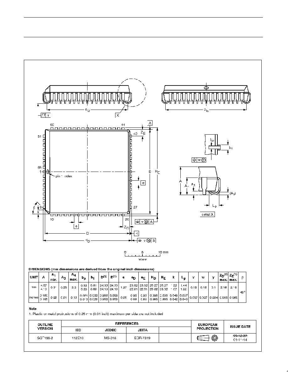
PLCC68:
plastic leaded chip carrier; 68 leads
SOT188-2
Philips Semiconductors
Product data
80C552/83C552
Single-chip 8-bit microcontroller with 10-bit A/D,
capture/compare timer, high-speed outputs, PWM
2002 Sep 03
22
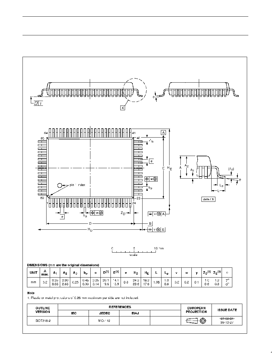
QFP80:
plastic quad flat package; 80 leads (lead length 1.95 mm); body 14 x 20 x 2.8 mm
SOT318-2

Philips Semiconductors
Product data
80C552/83C552
Single-chip 8-bit microcontroller with 10-bit A/D,
capture/compare timer, high-speed outputs, PWM
2002 Sep 03
23
Purchase of Philips I
2
C components conveys a license under the Philips' I
2
C patent
to use the components in the I
2
C system provided the system conforms to the
I
2
C specifications defined by Philips. This specification can be ordered using the
code 9398 393 40011.
Definitions
Short-form specification -- The data in a short-form specification is extracted from a full data sheet with the same type number and title. For
detailed information see the relevant data sheet or data handbook.
Limiting values definition -- Limiting values given are in accordance with the Absolute Maximum Rating System (IEC 60134). Stress above one
or more of the limiting values may cause permanent damage to the device. These are stress ratings only and operation of the device at these or
at any other conditions above those given in the Characteristics sections of the specification is not implied. Exposure to limiting values for extended
periods may affect device reliability.
Application information -- Applications that are described herein for any of these products are for illustrative purposes only. Philips
Semiconductors make no representation or warranty that such applications will be suitable for the specified use without further testing or
modification.
Disclaimers
Life support -- These products are not designed for use in life support appliances, devices or systems where malfunction of these products can
reasonably be expected to result in personal injury. Philips Semiconductors customers using or selling these products for use in such applications
do so at their own risk and agree to fully indemnify Philips Semiconductors for any damages resulting from such application.
Right to make changes -- Philips Semiconductors reserves the right to make changes, without notice, in the products, including circuits, standard
cells, and/or software, described or contained herein in order to improve design and/or performance. Philips Semiconductors assumes no
responsibility or liability for the use of any of these products, conveys no license or title under any patent, copyright, or mask work right to these
products, and makes no representations or warranties that these products are free from patent, copyright, or mask work right infringement, unless
otherwise specified.
Contact information
For additional information please visit
http://www.semiconductors.philips.com.
Fax: +31 40 27 24825
For sales offices addresses send e-mail to:
sales.addresses@www.semiconductors.philips.com.
©
Koninklijke Philips Electronics N.V. 2002
All rights reserved. Printed in U.S.A.
Date of release: 09-02
Document order number:
9397 750 10294
Philips
Semiconductors
Data sheet status
[1]
Objective data
Preliminary data
Product data
Product
status
[2]
Development
Qualification
Production
Definitions
This data sheet contains data from the objective specification for product development.
Philips Semiconductors reserves the right to change the specification in any manner without notice.
This data sheet contains data from the preliminary specification. Supplementary data will be
published at a later date. Philips Semiconductors reserves the right to change the specification
without notice, in order to improve the design and supply the best possible product.
This data sheet contains data from the product specification. Philips Semiconductors reserves the
right to make changes at any time in order to improve the design, manufacturing and supply.
Changes will be communicated according to the Customer Product/Process Change Notification
(CPCN) procedure SNW-SQ-650A.
Data sheet status
[1] Please consult the most recently issued data sheet before initiating or completing a design.
[2] The product status of the device(s) described in this data sheet may have changed since this data sheet was published. The latest information is available on the Internet at URL
http://www.semiconductors.philips.com.