 | –≠–ª–µ–∫—Ç—Ä–æ–Ω–Ω—ã–π –∫–æ–º–ø–æ–Ω–µ–Ω—Ç: 80C58X2 | –°–∫–∞—á–∞—Ç—å:  PDF PDF  ZIP ZIP |
Document Outline
- DESCRIPTION
- SELECTION TABLE
- FEATURES
- P80C31/32X2 ORDERING INFORMATION (ROMLESS)
- P87C51X2 ORDERING INFORMATION (4 KBYTE OTP)
- P87C52X2 ORDERING INFORMATION (8 KBYTE OTP)
- P87C54X2 ORDERING INFORMATION (16 KBYTE OTP)
- P87C58X2 ORDERING INFORMATION (32 KBYTE OTP)
- PART NUMBER DERIVATION
- BLOCK DIAGRAM 1
- BLOCK DIAGRAM 2 (CPU-ORIENTED)
- LOGIC SYMBOL
- PLASTIC DUAL IN-LINE PACKAGE PIN CONFIGURATIONS
- PLASTIC LEADED CHIP CARRIER PIN FUNCTIONS
- PLASTIC THIN SHRINK SMALL OUTLINE PACK PIN FUNCTIONS
- LOW PROFILE QUAD FLAT PACK PIN FUNCTIONS
- PIN DESCRIPTIONS
- OSCILLATOR CHARACTERISTICS
- LOW POWER MODES
- TIMER 0 AND TIMER 1 OPERATION
- TIMER 2 OPERATION
- FULL-DUPLEX ENHANCED UART
- ABSOLUTE MAXIMUM RATINGS 1, 2, 3
- AC ELECTRICAL CHARACTERISTICS
- DC ELECTRICAL CHARACTERISTICS
- DC ELECTRICAL CHARACTERISTICS
- AC ELECTRICAL CHARACTERISTICS (12-CLOCK MODE, 5 V ±10% OPERATION)
- AC ELECTRICAL CHARACTERISTICS (12-CLOCK MODE, 2.7 V TO 5.5 V OPERATION)
- AC ELECTRICAL CHARACTERISTICS (6-CLOCK MODE, 5 V ±10% OPERATION)
- AC ELECTRICAL CHARACTERISTICS (6-CLOCK MODE, 2.7 V TO 5.5 V OPERATION)
- EXPLANATION OF THE AC SYMBOLS
- EPROM CHARACTERISTICS
- PROGRAMMING AND VERIFICATION CHARACTERISTICS
- MASK ROM DEVICES
- 80C51X2 ROM CODE SUBMISSION
- 80C52X2 ROM CODE SUBMISSION
- 80C54X2 ROM CODE SUBMISSION
- 80C58X2 ROM CODE SUBMISSION
- PACKAGE OUTLINE
- SOT129-1
- SOT187-2
- SOT389-1
- SOT510-1
- REVISION HISTORY
- Data sheet status
- Definitions
- Disclaimers

Philips
Semiconductors
≠
P80C31X2/32X2
P80C51X2/52X2/54X2/58X2
P87C51X2/52X2/54X2/58X2
80C51 8-bit microcontroller family
4K/8K/16K/32K ROM/OTP
128B/256B RAM
low voltage (2.7 to 5.5 V), low power, high speed (30/33 MHz)
Product data
Supersedes data of 2002 Sep 12
2003 Jan 24
INTEGRATED CIRCUITS
Philips Semiconductors
Product data
P80C3xX2; P80C5xX2;
P87C5xX2
80C51 8-bit microcontroller family
4K/8K/16K/32K ROM/OTP, low voltage (2.7 to 5.5 V),
low power, high speed (30/33 MHz)
2
2003 Jan 24
853-2337 29260
DESCRIPTION
The Philips microcontrollers described in this data sheet are
high-performance static 80C51 designs incorporating Philips'
high-density CMOS technology with operation from 2.7 V to 5.5 V.
They support both 6-clock and 12-clock operation.
The P8xC31X2/51X2 and P8xC32X2/52X2/54X2/58X2 contain
128 byte RAM and 256 byte RAM respectively, 32 I/O lines, three
16-bit counter/timers, a six-source, four-priority level nested interrupt
structure, a serial I/O port for either multi-processor
communications, I/O expansion or full duplex UART, and on-chip
oscillator and clock circuits.
In addition, the devices are low power static designs which offer a
wide range of operating frequencies down to zero. Two software
selectable modes of power reduction -- idle mode and power-down
mode -- are available. The idle mode freezes the CPU while
allowing the RAM, timers, serial port, and interrupt system to
continue functioning. The power-down mode saves the RAM
contents but freezes the oscillator, causing all other chip functions to
be inoperative. Since the design is static, the clock can be stopped
without loss of user data. Then the execution can be resumed from
the point the clock was stopped.
SELECTION TABLE
For applications requiring more ROM and RAM, as well as more
on-chip peripherals, see the P89C66x and P89C51Rx2 data sheets.
Type
Memory
Timers
Serial Interfaces
RAM
ROM
OTP
Flash
# of
T
imers
PWM
PCA
WD
UART
I
2
C
CAN
SPI
ADC bits/ch.
I/O Pins
Interrupts
(External)
Program
Security
Default Clock
Rate
Optional
Clock Rate
Max.
Freq.
at 6-clk
/ 12-clk
(MHz)
Freq.
Range
at 3V
(MHz)
Freq.
Range
at 5V
(MHz)
P87C58X2
256B
≠
32K
≠
3
≠
≠
≠
n
≠
≠
≠
≠
32
6 (2)
n
12≠clk
6-clk
30/33
0≠16
0≠30/33
P80C58X2
256B
32K
≠
≠
3
≠
≠
≠
n
≠
≠
≠
≠
32
6 (2)
n
12≠clk
6-clk
30/33
0≠16
0≠30/33
P87C54X2
256B
≠
16K
≠
3
≠
≠
≠
n
≠
≠
≠
≠
32
6 (2)
n
12≠clk
6-clk
30/33
0≠16
0≠30/33
P80C54X2
256B
16K
≠
≠
3
≠
≠
≠
n
≠
≠
≠
≠
32
6 (2)
n
12≠clk
6-clk
30/33
0≠16
0≠30/33
P87C52X2
256B
≠
8K
≠
3
≠
≠
≠
n
≠
≠
≠
≠
32
6 (2)
n
12≠clk
6-clk
30/33
0≠16
0≠30/33
P80C52X2
256B
8K
≠
≠
3
≠
≠
≠
n
≠
≠
≠
≠
32
6 (2)
n
12≠clk
6-clk
30/33
0≠16
0≠30/33
P87C51X2
128B
≠
4K
≠
3
≠
≠
≠
n
≠
≠
≠
≠
32
6 (2)
n
12≠clk
6-clk
30/33
0≠16
0≠30/33
P80C51X2
128B
4K
≠
≠
3
≠
≠
≠
n
≠
≠
≠
≠
32
6 (2)
n
12≠clk
6-clk
30/33
0≠16
0≠30/33
P80C32X2
256B
≠
≠
≠
3
≠
≠
≠
n
≠
≠
≠
≠
32
6 (2)
≠
12≠clk
6-clk
30/33
0≠16
0≠30/33
P80C31X2
128B
≠
≠
≠
3
≠
≠
≠
n
≠
≠
≠
≠
32
6 (2)
≠
12≠clk
6-clk
30/33
0≠16
0≠30/33
NOTE:
1. I
2
C = Inter-Integrated Circuit Bus; CAN = Controller Area Network; SPI = Serial Peripheral Interface; PCA = Programmable Counter Array;
ADC = Analog-to-Digital Converter; PWM = Pulse Width Modulation

Philips Semiconductors
Product data
P80C3xX2; P80C5xX2;
P87C5xX2
80C51 8-bit microcontroller family
4K/8K/16K/32K ROM/OTP, low voltage (2.7 to 5.5 V),
low power, high speed (30/33 MHz)
2003 Jan 24
3
FEATURES
∑
80C51 Central Processing Unit
≠ 4 kbytes ROM/EPROM (P80/P87C51X2)
≠ 8 kbytes ROM/EPROM (P80/P87C52X2)
≠ 16 kbytes ROM/EPROM (P80/P87C54X2)
≠ 32 kbytes ROM/EPROM (P80/P87C58X2)
≠ 128 byte RAM (P80/P87C51X2 and P80C31X2)
≠ 256 byte RAM (P80/P87C52/54X2/58X2 and P80C32X2)
≠ Boolean processor
≠ Fully static operation
≠ Low voltage (2.7 V to 5.5 V at 16 MHz) operation
∑
12-clock operation with selectable 6-clock operation (via software
or via parallel programmer)
∑
Memory addressing capability
≠ Up to 64 kbytes ROM and 64 kbytes RAM
∑
Power control modes:
≠ Clock can be stopped and resumed
≠ Idle mode
≠ Power-down mode
∑
CMOS and TTL compatible
∑
Two speed ranges at V
CC
= 5 V
≠ 0 to 30 MHz with 6-clock operation
≠ 0 to 33 MHz with 12-clock operation
∑
PLCC, DIP, TSSOP or LQFP packages
∑
Extended temperature ranges
∑
Dual Data Pointers
∑
Security bits:
≠ ROM (2 bits)
≠ OTP (3 bits)
∑
Encryption array - 64 bytes
∑
Four interrupt priority levels
∑
Six interrupt sources
∑
Four 8-bit I/O ports
∑
Full-duplex enhanced UART
≠ Framing error detection
≠ Automatic address recognition
∑
Three 16-bit timers/counters T0, T1 (standard 80C51) and
additional T2 (capture and compare)
∑
Programmable clock-out pin
∑
Asynchronous port reset
∑
Low EMI (inhibit ALE, slew rate controlled outputs, and 6-clock
mode)
∑
Wake-up from Power Down by an external interrupt.
Philips Semiconductors
Product data
P80C3xX2; P80C5xX2;
P87C5xX2
80C51 8-bit microcontroller family
4K/8K/16K/32K ROM/OTP, low voltage (2.7 to 5.5 V),
low power, high speed (30/33 MHz)
2003 Jan 24
4
P80C31/32X2 ORDERING INFORMATION (ROMLESS)
Type number
Package
Temperature
R
(
∞
C)
Name
Description
Version
Range (
∞
C)
¡¡¡¡¡
¡¡¡¡¡
P80C31X2BA
PLCC44
plastic leaded chip carrier; 44 leads
¡¡¡¡¡
¡¡¡¡¡
SOT187-2
0 to +70
¡¡¡¡¡
¡¡¡¡¡
P80C31X2BN
DIP40
plastic dual in-line package; 40 leads (600 mil)
¡¡¡¡¡
¡¡¡¡¡
SOT129-1
0 to +70
¡¡¡¡¡
¡¡¡¡¡
P80C32X2BA
PLCC44
plastic leaded chip carrier; 44 leads
¡¡¡¡¡
¡¡¡¡¡
SOT187-2
0 to +70
¡¡¡¡¡
P80C32X2BN
DIP40
plastic dual in-line package; 40 leads (600 mil)
¡¡¡¡¡
SOT129-1
0 to +70
¡¡¡¡¡
¡¡¡¡¡
P80C32X2BBD
LQFP44
plastic low profile quad flat package; 44 leads; body 10 x 10 x 1.4 mm
¡¡¡¡¡
¡¡¡¡¡
SOT389-1
0 to +70
¡¡¡¡¡
¡¡¡¡¡
P80C32X2FA
PLCC44
plastic leaded chip carrier; 44 leads
¡¡¡¡¡
¡¡¡¡¡
SOT187-2
≠40 to +85
¡¡¡¡¡
¡¡¡¡¡
P80C32X2FN
DIP40
plastic dual in-line package; 40 leads (600 mil)
¡¡¡¡¡
¡¡¡¡¡
SOT129-1
≠40 to +85
P87C51X2 ORDERING INFORMATION (4 KBYTE OTP)
Type number
Package
Temperature
R
(
∞
C)
Name
Description
Version
Range (
∞
C)
P87C51X2BA
PLCC44
plastic leaded chip carrier; 44 leads
SOT187-2
0 to +70
P87C51X2BN
DIP40
plastic dual in-line package; 40 leads (600 mil)
SOT129-1
0 to +70
P87C51X2BBD
LQFP44
plastic low profile quad flat package; 44 leads; body 10 x 10 x 1.4 mm
SOT389-1
0 to +70
P87C51X2FA
PLCC44
plastic leaded chip carrier; 44 leads
SOT187-2
≠40 to +85
P87C51X2FBD
LQFP44
plastic low profile quad flat package; 44 leads; body 10 x 10 x 1.4 mm
SOT389-1
≠40 to +85
P87C52X2 ORDERING INFORMATION (8 KBYTE OTP)
Type number
Package
Temperature
R
(
∞
C)
Name
Description
Version
Range (
∞
C)
P87C52X2BA
PLCC44
plastic leaded chip carrier; 44 leads
SOT187-2
0 to +70
P87C52X2BN
DIP40
plastic dual in-line package; 40 leads (600 mil)
SOT129-1
0 to +70
P87C52X2BBD
LQFP44
plastic low profile quad flat package; 44 leads; body 10 x 10 x 1.4 mm
SOT389-1
0 to +70
P87C52X2FA
PLCC44
plastic leaded chip carrier; 44 leads
SOT187-2
≠40 to +85
P87C52X2FN
DIP40
plastic dual in-line package; 40 leads (600 mil)
SOT129-1
≠40 to +85
P87C52X2FBD
LQFP44
plastic low profile quad flat package; 44 leads; body 10 x 10 x 1.4 mm
SOT389-1
≠40 to +85
P87C54X2 ORDERING INFORMATION (16 KBYTE OTP)
Type number
Package
Temperature
R
(
∞
C)
Name
Description
Version
Range (
∞
C)
¡¡¡¡¡
¡¡¡¡¡
P87C54X2BA
¡¡¡¡¡
¡¡¡¡¡
PLCC44
¡¡¡¡¡¡¡¡¡¡¡¡¡¡¡¡¡¡
¡¡¡¡¡¡¡¡¡¡¡¡¡¡¡¡¡¡
plastic lead chip carrier; 44 leads
¡¡¡¡¡
¡¡¡¡¡
SOT187-2
¡¡¡¡¡
¡¡¡¡¡
0 to +70
¡¡¡¡¡
¡¡¡¡¡
P87C54X2BN
¡¡¡¡¡
¡¡¡¡¡
DIP40
¡¡¡¡¡¡¡¡¡¡¡¡¡¡¡¡¡¡
¡¡¡¡¡¡¡¡¡¡¡¡¡¡¡¡¡¡
plastic dual in-line package; 40 leads (600 mil)
¡¡¡¡¡
¡¡¡¡¡
SOT129-1
¡¡¡¡¡
¡¡¡¡¡
0 to +70
P87C54X2BBD
LQFP44
plastic low profile quad flat package; 44 leads; body 10 x 10 x 1.4 mm
SOT389-1
0 to +70
P87C54X2BDH
TSSOP38
plastic thin shrink small outline package; 38 leads; body width 4.4 mm;
lead pitch 0.5 mm
SOT510-1
0 to +70
¡¡¡¡¡
¡¡¡¡¡
P87C54X2FA
¡¡¡¡¡
¡¡¡¡¡
PLCC44
¡¡¡¡¡¡¡¡¡¡¡¡¡¡¡¡¡¡
¡¡¡¡¡¡¡¡¡¡¡¡¡¡¡¡¡¡
plastic lead chip carrier; 44 leads
¡¡¡¡¡
¡¡¡¡¡
SOT187-2
¡¡¡¡¡
¡¡¡¡¡
≠40 to +85
P87C54X2FBD
LQFP44
plastic low profile quad flat package; 44 leads; body 10 x 10 x 1.4 mm
SOT389-1
≠40 to +85
P87C58X2 ORDERING INFORMATION (32 KBYTE OTP)
Type number
Package
Temperature
R
(
∞
C)
Name
Description
Version
Range (
∞
C)
¡¡¡¡¡
¡¡¡¡¡
P87C58X2BA
¡¡¡¡¡
¡¡¡¡¡
PLCC44
¡¡¡¡¡¡¡¡¡¡¡¡¡¡¡¡¡¡
¡¡¡¡¡¡¡¡¡¡¡¡¡¡¡¡¡¡
plastic lead chip carrier; 44 leads
¡¡¡¡¡
¡¡¡¡¡
SOT187-2
¡¡¡¡¡
¡¡¡¡¡
0 to +70
¡¡¡¡¡
¡¡¡¡¡
P87C58X2BN
¡¡¡¡¡
¡¡¡¡¡
DIP40
¡¡¡¡¡¡¡¡¡¡¡¡¡¡¡¡¡¡
¡¡¡¡¡¡¡¡¡¡¡¡¡¡¡¡¡¡
plastic dual in-line package; 40 leads (600 mil)
¡¡¡¡¡
¡¡¡¡¡
SOT129-1
¡¡¡¡¡
¡¡¡¡¡
0 to +70
P87C58X2BBD
LQFP44
plastic low profile quad flat package; 44 leads; body 10 x 10 x 1.4 mm
SOT389-1
0 to +70
¡¡¡¡¡
P87C58X2FA
¡¡¡¡¡
PLCC44
¡¡¡¡¡¡¡¡¡¡¡¡¡¡¡¡¡¡
plastic lead chip carrier; 44 leads
¡¡¡¡¡
SOT187-2
¡¡¡¡¡
≠40 to +85
P87C58X2FBD
LQFP44
plastic low profile quad flat package; 44 leads; body 10 x 10 x 1.4 mm
SOT389-1
≠40 to +85
¡¡¡¡¡
¡¡¡¡¡
P87C58X2FN
¡¡¡¡¡
¡¡¡¡¡
DIP40
¡¡¡¡¡¡¡¡¡¡¡¡¡¡¡¡¡¡
¡¡¡¡¡¡¡¡¡¡¡¡¡¡¡¡¡¡
plastic dual in-line package; 40 leads (600 mil)
¡¡¡¡¡
¡¡¡¡¡
SOT129-1
¡¡¡¡¡
¡¡¡¡¡
≠40 to +85
All OTP parts listed here are also available as ROM parts (80C5xX2). Please contact your Philips representative if you would like to order a
ROM part.

Philips Semiconductors
Product data
P80C3xX2; P80C5xX2;
P87C5xX2
80C51 8-bit microcontroller family
4K/8K/16K/32K ROM/OTP, low voltage (2.7 to 5.5 V),
low power, high speed (30/33 MHz)
2003 Jan 24
5
PART NUMBER DERIVATION
Memory
Temperature Range
Package
P87C51X2
7 =
OTP
0 =
ROM or
ROMless
5 = ROM/OTP
3 = ROMless
1 =
128 BYTES RAM
4 KBYTES ROM/OTP
2 =
256 BYTES RAM
8 KBYTES ROM/OTP
4 =
256 BYTES RAM
16 KBYTES ROM/OTP
8 =
256 BYTES RAM
32 KBYTES ROM/OTP
X2 = 6-clock
mode available
B = 0
∞
C TO +70
∞
C
F = ≠40
∞
C TO +85
∞
C
A = PLCC
N = DIP
BD = LQFP
DH = TSSOP
The following table illustrates the correlation between operating mode, power supply and maximum external clock frequency:
Operating Mode
Power Supply
Maximum Clock Frequency
6-clock
5 V
±
10%
30 MHz
6-clock
2.7 V to 5.5 V
16 MHz
12-clock
5 V
±
10%
33 MHz
12-clock
2.7 V to 5.5 V
16 MHz
Philips Semiconductors
Product data
P80C3xX2; P80C5xX2;
P87C5xX2
80C51 8-bit microcontroller family
4K/8K/16K/32K ROM/OTP, low voltage (2.7 to 5.5 V),
low power, high speed (30/33 MHz)
2003 Jan 24
6
BLOCK DIAGRAM 1
su01579
Accelerated 80C51 CPU
(12-clk mode, 6-clk mode)
0K / 4K / 8K / 16K /
32 kbyte
CODE ROM / EPROM
128 / 256 Byte
Data RAM
Port 3
Configurable I/Os
Port 2
Configurable I/Os
Port 1
Configurable I/Os
Port 0
Configurable I/Os
Oscillator
Crystal or
Resonator
Full-duplex enhanced
UART
Timer 0
Timer 1
Timer 2
Philips Semiconductors
Product data
P80C3xX2; P80C5xX2;
P87C5xX2
80C51 8-bit microcontroller family
4K/8K/16K/32K ROM/OTP, low voltage (2.7 to 5.5 V),
low power, high speed (30/33 MHz)
2003 Jan 24
7
BLOCK DIAGRAM 2 (CPU-ORIENTED)
su01723
PSEN
EA / V
PP
ALE/PROG
RST
XTAL1
XTAL2
VCC
VSS
PORT 0
DRIVERS
PORT 2
DRIVERS
RAM ADDR
REGISTER
RAM
PORT 0
LATCH
PORT 2
LATCH
ROM/EPROM
REGISTER
B
ACC
STACK
POINTER
TMP2
TMP1
ALU
TIMING
AND
CONTROL
INSTRUCTION
REGISTER
PD
OSCILLATOR
PSW
PORT 1
LATCH
PORT 3
LATCH
PORT 1
DRIVERS
PORT 3
DRIVERS
PROGRAM
ADDRESS
REGISTER
BUFFER
PC
INCRE-
MENTER
PROGRAM
COUNTER
DPTR'S
MULTIPLE
P1.0≠P1.7
P3.0≠P3.7
1
P0.0≠P0.7
P2.0≠P2.7
SFRs
TIMERS
8
8
16
NOTE:
1. P3.2 and P3.5 absent in the TSSOP38 package.
Philips Semiconductors
Product data
P80C3xX2; P80C5xX2;
P87C5xX2
80C51 8-bit microcontroller family
4K/8K/16K/32K ROM/OTP, low voltage (2.7 to 5.5 V),
low power, high speed (30/33 MHz)
2003 Jan 24
8
LOGIC SYMBOL
POR
T
0
POR
T
1
POR
T
2
POR
T
3
ADDRESS AND
DATA BUS
ADDRESS BUS
T2
T2EX
RxD
TxD
INT0
1
INT1
T0
T1
1
WR
RD
SECONDAR
Y
FUNCTIONS
RST
EA/V
PP
PSEN
ALE/PROG
V
SS
V
CC
XTAL1
XTAL2
SU01724
NOTE:
1. INT0/P3.2 and T1/P3.5 are absent in the TSSOP38 package.
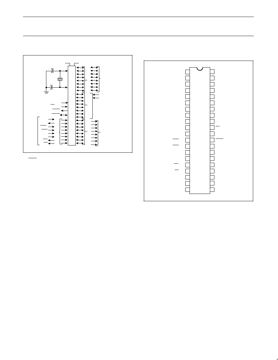
PLASTIC DUAL IN-LINE PACKAGE
PIN CONFIGURATIONS
SU01063
1
2
3
4
5
6
7
8
9
10
11
12
13
14
15
16
17
18
19
20
21
22
23
24
25
26
27
28
29
30
31
32
33
34
35
36
37
38
39
40
T2/P1.0
T2EX/P1.1
P1.2
P1.3
P1.4
P1.5
P1.6
RST
RxD/P3.0
TxD/P3.1
INT0/P3.2
INT1/P3.3
T0/P3.4
T1/P3.5
P1.7
WR/P3.6
RD/P3.7
XTAL2
XTAL1
V
SS
P2.0/A8
P2.1/A9
P2.2/A10
P2.3/A11
P2.4/A12
P2.5/A13
P2.6/A14
P2.7/A15
PSEN
ALE
EA/V
PP
P0.7/AD7
P0.6/AD6
P0.5/AD5
P0.4/AD4
P0.3/AD3
P0.2/AD2
P0.1/AD1
P0.0/AD0
V
CC
DUAL
IN-LINE
PACKAGE
Philips Semiconductors
Product data
P80C3xX2; P80C5xX2;
P87C5xX2
80C51 8-bit microcontroller family
4K/8K/16K/32K ROM/OTP, low voltage (2.7 to 5.5 V),
low power, high speed (30/33 MHz)
2003 Jan 24
9
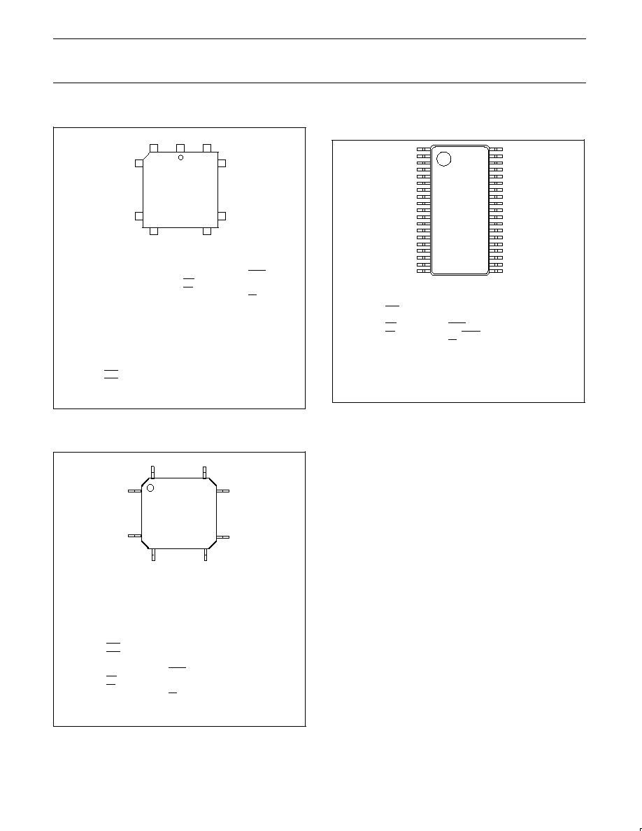
PLASTIC LEADED CHIP CARRIER PIN FUNCTIONS
SU01062
PLCC
6
1
40
7
17
39
29
18
28
Pin
Function
1
NIC*
2
P1.0/T2
3
P1.1/T2EX
4
P1.2
5
P1.3
6
P1.4
7
P1.5
8
P1.6
9
P1.7
10
RST
11
P3.0/RxD
12
NIC*
13
P3.1/TxD
14
P3.2/INT0
15
P3.3/INT1
Pin
Function
16
P3.4/T0
17
P3.5/T1
18
P3.6/WR
19
P3.7/RD
20
XTAL2
21
XTAL1
22
V
SS
23
NIC*
24
P2.0/A8
25
P2.1/A9
26
P2.2/A10
27
P2.3/A11
28
P2.4/A12
29
P2.5/A13
30
P2.6/A14
Pin
Function
31
P2.7/A15
32
PSEN
33
ALE
34
NIC*
35
EA/V
PP
36
P0.7/AD7
37
P0.6/AD6
38
P0.5/AD5
39
P0.4/AD4
40
P0.3/AD3
41
P0.2/AD2
42
P0.1/AD1
43
P0.0/AD0
44
V
CC
* NO INTERNAL CONNECTION
LOW PROFILE QUAD FLAT PACK
PIN FUNCTIONS
SU01487
LQFP
44
34
1
11
33
23
12
22
Pin
Function
1
P1.5
2
P1.6
3
P1.7
4
RST
5
P3.0/RxD
6
NIC*
7
P3.1/TxD
8
P3.2/INT0
9
P3.3/INT1
10
P3.4/T0
11
P3.5/T1
12
P3.6/WR
13
P3.7/RD
14
XTAL2
15
XTAL1
Pin
Function
16
V
SS
17
NIC*
18
P2.0/A8
19
P2.1/A9
20
P2.2/A10
21
P2.3/A11
22
P2.4/A12
23
P2.5/A13
24
P2.6/A14
25
P2.7/A15
26
PSEN
27
ALE
28
NIC*
29
EA/V
PP
30
P0.7/AD7
Pin
Function
31
P0.6/AD6
32
P0.5/AD5
33
P0.4/AD4
34
P0.3/AD3
35
P0.2/AD2
36
P0.1/AD1
37
P0.0/AD0
38
V
CC
39
NIC*
40
P1.0/T2
41
P1.1/T2EX
42
P1.2
43
P1.3
44
P1.4
* NO INTERNAL CONNECTION
PLASTIC THIN SHRINK SMALL OUTLINE PACK
PIN FUNCTIONS
su01725
Pin
Function
1
P3.0/RxD
2
P3.1/TxD
3
P3.3/INT1
4
P3.4/T0
5
P3.6/WR
6
P3.7/RD
7
XTAL2
8
XTAL1
9
V
SS
10
P2.0/A8
11
P2.1/A9
12
P2.2/A10
13
P2.3/A11
Pin
Function
14
P2.4/A12
15
P2.5/A13
16
P2.6/A14
17
P2.7/A15
18
PSEN
19
ALE/PROG
20
EA/V
PP
21
P0.7/AD7
22
P0.6/AD6
23
P0.5/AD5
24
P0.4/AD4
25
P0.3/AD3
26
P0.2/AD2
Pin
Function
27
P0.1/AD1
28
P0.0/AD0
29
V
DD
30
P1.0/T2
31
P1.1/T2EX
32
P1.2
33
P1.3
34
P1.4
35
P1.5
36
P1.6
37
P1.7
38
RST
1
19
20
38
TSSOP
Philips Semiconductors
Product data
P80C3xX2; P80C5xX2;
P87C5xX2
80C51 8-bit microcontroller family
4K/8K/16K/32K ROM/OTP, low voltage (2.7 to 5.5 V),
low power, high speed (30/33 MHz)
2003 Jan 24
10
PIN DESCRIPTIONS
PIN NUMBER
MNEMONIC
DIP
PLCC
LQFP
TSSOP
TYPE
NAME AND FUNCTION
V
SS
20
22
16
9
I
Ground: 0 V reference.
V
CC
40
44
38
29
I
Power Supply: This is the power supply voltage for normal, idle, and power-down
operation.
P0.0-0.7
39≠32
43≠36
37≠30
28≠21
I/O
Port 0: Port 0 is an open-drain, bidirectional I/O port. Port 0 pins that have 1s
written to them float and can be used as high-impedance inputs. Port 0 is also the
multiplexed low-order address and data bus during accesses to external program
and data memory. In this application, it uses strong internal pull-ups when emitting
1s. Port 0 also outputs the code bytes during program verification and received
code bytes during EPROM programming. External pull-ups are required during
program verification.
P1.0≠P1.7
1≠8
2≠9
40≠44,
1≠3
30≠37
I/O
Port 1: Port 1 is an 8-bit bidirectional I/O port with internal pull-ups. Port 1 pins that
have 1s written to them are pulled high by the internal pull-ups and can be used as
inputs. As inputs, port 1 pins that are externally pulled low will source current
because of the internal pull-ups. (See DC Electrical Characteristics: I
IL
). Port 1 also
receives the low-order address byte during program memory verification. Alternate
functions for Port 1 include:
1
2
40
30
I/O
T2 (P1.0): Timer/Counter 2 external count input/clockout (see Programmable
Clock-Out)
2
3
41
31
I
T2EX (P1.1): Timer/Counter 2 Reload/Capture/Direction control
P2.0≠P2.7
21≠28
24≠31
18≠25
10≠17
I/O
Port 2: Port 2 is an 8-bit bidirectional I/O port with internal pull-ups. Port 2 pins that
have 1s written to them are pulled high by the internal pull-ups and can be used as
inputs. As inputs, port 2 pins that are externally being pulled low will source current
because of the internal pull-ups. (See DC Electrical Characteristics: I
IL
). Port 2
emits the high-order address byte during fetches from external program memory
and during accesses to external data memory that use 16-bit addresses (MOVX
@DPTR). In this application, it uses strong internal pull-ups when emitting 1s.
During accesses to external data memory that use 8-bit addresses (MOV @Ri), port
2 emits the contents of the P2 special function register. Some Port 2 pins receive
the high order address bits during EPROM programming and verification.
P3.0≠P3.7
10≠17
11,
13≠19
5,
7≠13
1≠6
I/O
Port 3: Port 3 is an 8-bit bidirectional I/O port with internal pull-ups. Port 3 pins that
have 1s written to them are pulled high by the internal pull-ups and can be used as
inputs. As inputs, port 3 pins that are externally being pulled low will source current
because of the pull-ups. (See DC Electrical Characteristics: I
IL
). Port 3 also serves
the special features of the 80C51 family, as listed below:
10
11
5
1
I
RxD (P3.0): Serial input port
11
13
7
2
O
TxD (P3.1): Serial output port
12
14
8
I
INT0 (P3.2): External interrupt
1
13
15
9
3
I
INT1 (P3.3): External interrupt
14
16
10
4
I
T0 (P3.4): Timer 0 external input
15
17
11
I
T1 (P3.5): Timer 1 external input
1
16
18
12
5
O
WR (P3.6): External data memory write strobe
17
19
13
6
O
RD (P3.7): External data memory read strobe
RST
9
10
4
38
I
Reset: A high on this pin for two machine cycles while the oscillator is running,
resets the device. An internal diffused resistor to V
SS
permits a power-on reset
using only an external capacitor to V
CC
.
ALE/PROG
30
33
27
19
O
Address Latch Enable/Program Pulse: Output pulse for latching the low byte of
the address during an access to external memory. In normal operation, ALE is
emitted at a constant rate of 1/6 (12-clock Mode) or 1/3 (6-clock Mode) the
oscillator frequency, and can be used for external timing or clocking. Note that one
ALE pulse is skipped during each access to external data memory. This pin is also
the program pulse input (PROG) during EPROM programming. ALE can be
disabled by setting SFR auxiliary.0. With this bit set, ALE will be active only during
a MOVX instruction.
Philips Semiconductors
Product data
P80C3xX2; P80C5xX2;
P87C5xX2
80C51 8-bit microcontroller family
4K/8K/16K/32K ROM/OTP, low voltage (2.7 to 5.5 V),
low power, high speed (30/33 MHz)
2003 Jan 24
11
PIN NUMBER
MNEMONIC
NAME AND FUNCTION
TYPE
TSSOP
LQFP
PLCC
DIP
PSEN
29
32
26
18
O
Program Store Enable: The read strobe to external program memory. When the
device is executing code from the external program memory, PSEN is activated
twice each machine cycle, except that two PSEN activations are skipped during
each access to external data memory. PSEN is not activated during fetches from
internal program memory.
EA/V
PP
31
35
29
20
I
External Access Enable/Programming Supply Voltage: EA must be externally held low to enable
the device to fetch code from external program memory locations 0000H to
0FFFH/1FFFH/3FFFH/7FFFH. If EA is held high, the device executes from internal program memory
unless the program counter contains an address greater than the on-chip ROM/OTP. This pin also
receives the 12.75 V programming supply voltage (V
PP
) during EPROM programming. If security bit
1 is programmed, EA will be internally latched on Reset.
XTAL1
19
21
15
8
I
Crystal 1: Input to the inverting oscillator amplifier and input to the internal clock
generator circuits.
XTAL2
18
20
14
7
O
Crystal 2: Output from the inverting oscillator amplifier.
NOTES:
To avoid "latch-up" effect at power-on, the voltage on any pin at any time must not be higher than V
CC
+ 0.5 V or V
SS
≠ 0.5 V, respectively.
1. Absent in the TSSOP38 package.
Philips Semiconductors
Product data
P80C3xX2; P80C5xX2;
P87C5xX2
80C51 8-bit microcontroller family
4K/8K/16K/32K ROM/OTP, low voltage (2.7 to 5.5 V),
low power, high speed (30/33 MHz)
2003 Jan 24
12
Table 1.
Special Function Registers
SYMBOL
DESCRIPTION
DIRECT
ADDRESS
BIT ADDRESS, SYMBOL, OR ALTERNATIVE PORT FUNCTION
MSB LSB
RESET
VALUE
ACC*
Accumulator
E0H
E7
E6
E5
E4
E3
E2
E1
E0
00H
AUXR#
Auxiliary
8EH
≠
≠
≠
≠
≠
≠
≠
AO
xxxxxxx0B
AUXR1#
Auxiliary 1
A2H
≠
≠
≠
LPEP
2
WUPD
0
≠
DPS
xxx000x0B
B*
B register
F0H
F7
F6
F5
F4
F3
F2
F1
F0
00H
CKCON
Clock Control Register
8FH
≠
≠
≠
≠
≠
≠
≠
X2
xxx00000B
DPTR:
Data Pointer (2 bytes)
DPH
Data Pointer High
83H
00H
DPL
Data Pointer Low
82H
00H
AF
AE
AD
AC
AB
AA
A9
A8
IE*
Interrupt Enable
A8H
EA
≠
ET2
ES
ET1
EX1
ET0
EX0
0x000000B
BF
BE
BD
BC
BB
BA
B9
B8
IP*
Interrupt Priority
B8H
≠
≠
PT2
PS
PT1
PX1
PT0
PX0
xx000000B
IPH#
Interrupt Priority High
B7H
≠
≠
PT2H
PSH
PT1H
PX1H
PT0H
PX0H
xx000000B
87
86
85
84
83
82
81
80
P0*
Port 0
80H
AD7
AD6
AD5
AD4
AD3
AD2
AD1
AD0
FFH
97
96
95
94
93
92
91
90
P1*
Port 1
90H
≠
≠
≠
≠
≠
≠
T2EX
T2
FFH
A7
A6
A5
A4
A3
A2
A1
A0
P2*
Port 2
A0H
AD15
AD14
AD13
AD12
AD11
AD10
AD9
AD8
FFH
B7
B6
B5
B4
B3
B2
B1
B0
P3*
Port 3
B0H
RD
WR
T1
T0
INT1
INT0
TxD
RxD
FFH
PCON#
1
Power Control
87H
SMOD1
SMOD0
≠
POF
GF1
GF0
PD
IDL
00xx0000B
D7
D6
D5
D4
D3
D2
D1
D0
PSW*
Program Status Word
D0H
CY
AC
F0
RS1
RS0
OV
≠
P
000000x0B
RACAP2H
#
Timer 2 Capture High
CBH
00H
RACAP2L
#
Timer 2 Capture Low
CAH
00H
SADDR#
Slave Address
A9H
00H
SADEN#
Slave Address Mask
B9H
00H
SBUF
Serial Data Buffer
99H
xxxxxxxxB
9F
9E
9D
9C
9B
9A
99
98
SCON*
Serial Control
98H
SM0/FE
SM1
SM2
REN
TB8
RB8
TI
RI
00H
SP
Stack Pointer
81H
07H
8F
8E
8D
8C
8B
8A
89
88
TCON*
Timer Control
88H
TF1
TR1
TF0
TR0
IE1
IT1
IE0
IT0
00H
CF
CE
CD
CC
CB
CA
C9
C8
T2CON*
Timer 2 Control
C8H
TF2
EXF2
RCLK
TCLK
EXEN2
TR2
C/T2
CP/RL2
00H
T2MOD#
Timer 2 Mode Control
C9H
≠
≠
≠
≠
≠
≠
T2OE
DCEN
xxxxxx00B
TH0
Timer High 0
8CH
00H
TH1
Timer High 1
8DH
00H
TH2#
Timer High 2
CDH
00H
TL0
Timer Low 0
8AH
00H
TL1
Timer Low 1
8BH
00H
TL2#
Timer Low 2
CCH
00H
TMOD
Timer Mode
89H
GATE
C/T
M1
M0
GATE
C/T
M1
M0
00H
NOTE:
Unused register bits that are not defined should not be set by the user's program. If violated, the device could function incorrectly.
*
SFRs are bit addressable.
#
SFRs are modified from or added to the 80C51 SFRs.
≠
Reserved bits.
1. Reset value depends on reset source.
2. LPEP ≠ Low Power EPROM operation (OTP only)

Philips Semiconductors
Product data
P80C3xX2; P80C5xX2;
P87C5xX2
80C51 8-bit microcontroller family
4K/8K/16K/32K ROM/OTP, low voltage (2.7 to 5.5 V),
low power, high speed (30/33 MHz)
2003 Jan 24
13
OSCILLATOR CHARACTERISTICS
Using the oscillator
XTAL1 and XTAL2 are the input and output, respectively, of an
inverting amplifier. The pins can be configured for use as an on-chip
oscillator, as shown in the logic symbol.
To drive the device from an external clock source, XTAL1 should be
driven while XTAL2 is left unconnected. However, minimum and
maximum high and low times specified in the data sheet must be
observed.
Clock Control Register (CKCON)
This device provides control of the 6-clock/12-clock mode by both
an SFR bit (bit X2 in register CKCON and an OTP bit (bit OX2).
When X2 is 0, 12-clock mode is activated. By setting this bit to 1, the
system is switching to 6-clock mode. Having this option
implemented as SFR bit, it can be accessed anytime and changed
to either value. Changing X2 from 0 to 1 will result in executing user
code at twice the speed, since all system time intervals will be
divided by 2. Changing back from 6-clock to 12-clock mode will slow
down running code by a factor of 2.
The OTP clock control bit (OX2) activates the 6-clock mode when
programmed using a parallel programmer, superceding the X2 bit
(CKCON.0). Please also see Table 2 below.
Table 2.
OX2 clock mode bit
(can only be set by
parallel programmer)
X2 bit
(CKCON.0)
CPU clock mode
erased
0
12-clock mode
(default)
erased
1
6-clock mode
programmed
X
6-clock mode
Programmable Clock-Out
A 50% duty cycle clock can be programmed to be output on P1.0.
This pin, besides being a regular I/O pin, has two alternate
functions. It can be programmed:
1. to input the external clock for Timer/Counter 2, or
2. to output a 50% duty cycle clock ranging from 61 Hz to 4 MHz at
a 16 MHz operating frequency in 12-clock mode (122 Hz to
8 MHz in 6-clock mode).
To configure the Timer/Counter 2 as a clock generator, bit C/T2 (in
T2CON) must be cleared and bit T20E in T2MOD must be set. Bit
TR2 (T2CON.2) also must be set to start the timer.
The Clock-Out frequency depends on the oscillator frequency and
the reload value of Timer 2 capture registers (RCAP2H, RCAP2L)
as shown in this equation:
Oscillator Frequency
n
(65536≠RCAP2H, RCAP2L)
Where:
n = 2 in 6-clock mode, 4 in 12-clock mode.
(RCAP2H,RCAP2L) = the content of RCAP2H and RCAP2L
taken as a 16-bit unsigned integer.
In the Clock-Out mode Timer 2 roll-overs will not generate an
interrupt. This is similar to when it is used as a baud-rate generator.
It is possible to use Timer 2 as a baud-rate generator and a clock
generator simultaneously. Note, however, that the baud-rate and the
Clock-Out frequency will be the same.
RESET
A reset is accomplished by holding the RST pin HIGH for at least
two machine cycles (24 oscillator periods in 12-clock and 12
oscillator periods in 6-clock mode), while the oscillator is running. To
insure a reliable power-up reset, the RST pin must be high long
enough to allow the oscillator time to start up (normally a few
milliseconds) plus two machine cycles. After the reset, the part runs
in 12-clock mode, unless it has been set to 6-clock operation using a
parallel programmer.
LOW POWER MODES
Stop Clock Mode
The static design enables the clock speed to be reduced down to
0 MHz (stopped). When the oscillator is stopped, the RAM and
Special Function Registers retain their values. This mode allows
step-by-step utilization and permits reduced system power
consumption by lowering the clock frequency down to any value. For
lowest power consumption the Power Down mode is suggested.
Idle Mode
In idle mode (see Table 3), the CPU puts itself to sleep while all of
the on-chip peripherals stay active. The instruction to invoke the idle
mode is the last instruction executed in the normal operating mode
before the idle mode is activated. The CPU contents, the on-chip
RAM, and all of the special function registers remain intact during
this mode. The idle mode can be terminated either by any enabled
interrupt (at which time the process is picked up at the interrupt
service routine and continued), or by a hardware reset which starts
the processor in the same manner as a power-on reset.
Power-Down Mode
To save even more power, a Power Down mode (see Table 3) can
be invoked by software. In this mode, the oscillator is stopped and
the instruction that invoked Power Down is the last instruction
executed. The on-chip RAM and Special Function Registers retain
their values down to 2.0 V and care must be taken to return V
CC
to
the minimum specified operating voltages before the Power Down
Mode is terminated.
Either a hardware reset or external interrupt can be used to exit from
Power Down. Reset redefines all the SFRs but does not change the
on-chip RAM. An external interrupt allows both the SFRs and the
on-chip RAM to retain their values. WUPD (AUXR1.3≠Wakeup from
Power Down) enables or disables the wakeup from power down with
external interrupt. Where:
WUPD = 0: Disable
WUPD = 1: Enable
To properly terminate Power Down, the reset or external interrupt
should not be executed before V
CC
is restored to its normal
operating level and must be held active long enough for the
oscillator to restart and stabilize (normally less than 10 ms).
To terminate Power Down with an external interrupt, INT0 or INT1
must be enabled and configured as level-sensitive. Holding the pin
low restarts the oscillator but bringing the pin back high completes
the exit. Once the interrupt is serviced, the next instruction to be
executed after RETI will be the one following the instruction that put
the device into Power Down.
Philips Semiconductors
Product data
P80C3xX2; P80C5xX2;
P87C5xX2
80C51 8-bit microcontroller family
4K/8K/16K/32K ROM/OTP, low voltage (2.7 to 5.5 V),
low power, high speed (30/33 MHz)
2003 Jan 24
14
Low-Power EPROM operation (LPEP)
The EPROM array contains some analog circuits that are not
required when V
CC
is less than 4 V, but are required for a V
CC
greater than 4 V. The LPEP bit (AUXR.4), when set, will powerdown
these analog circuits resulting in a reduced supply current. This bit
should be set ONLY for applications that operate at a V
CC
less than
4 V.
Design Consideration
When the idle mode is terminated by a hardware reset, the device
normally resumes program execution from where it left off, up to two
machine cycles before the internal reset algorithm takes control.
On-chip hardware inhibits access to internal RAM in this event, but
access to the port pins is not inhibited. To eliminate the possibility of
an unexpected write when Idle is terminated by reset, the instruction
following the one that invokes Idle should not be one that writes to a
port pin or to external memory.
ONCE
TM
Mode
The ONCE ("On-Circuit Emulation") Mode facilitates testing and
debugging of systems without the device having to be removed from
the circuit. The ONCE Mode is invoked in the following way:
1. Pull ALE low while the device is in reset and PSEN is high;
2. Hold ALE low as RST is deactivated.
While the device is in ONCE Mode, the Port 0 pins go into a float
state, and the other port pins and ALE and PSEN are weakly pulled
high. The oscillator circuit remains active. While the device is in this
mode, an emulator or test CPU can be used to drive the circuit.
Normal operation is restored when a normal reset is applied.
Table 3. External Pin Status During Idle and Power-Down Modes
MODE
PROGRAM MEMORY
ALE
PSEN
PORT 0
PORT 1
PORT 2
PORT 3
Idle
Internal
1
1
Data
Data
Data
Data
Idle
External
1
1
Float
Data
Address
Data
Power-down
Internal
0
0
Data
Data
Data
Data
Power-down
External
0
0
Float
Data
Data
Data
TIMER 0 AND TIMER 1 OPERATION
Timer 0 and Timer 1
The "Timer" or "Counter" function is selected by control bits C/T in
the Special Function Register TMOD. These two Timer/Counters
have four operating modes, which are selected by bit-pairs (M1, M0)
in TMOD. Modes 0, 1, and 2 are the same for both Timers/Counters.
Mode 3 is different. The four operating modes are described in the
following text.
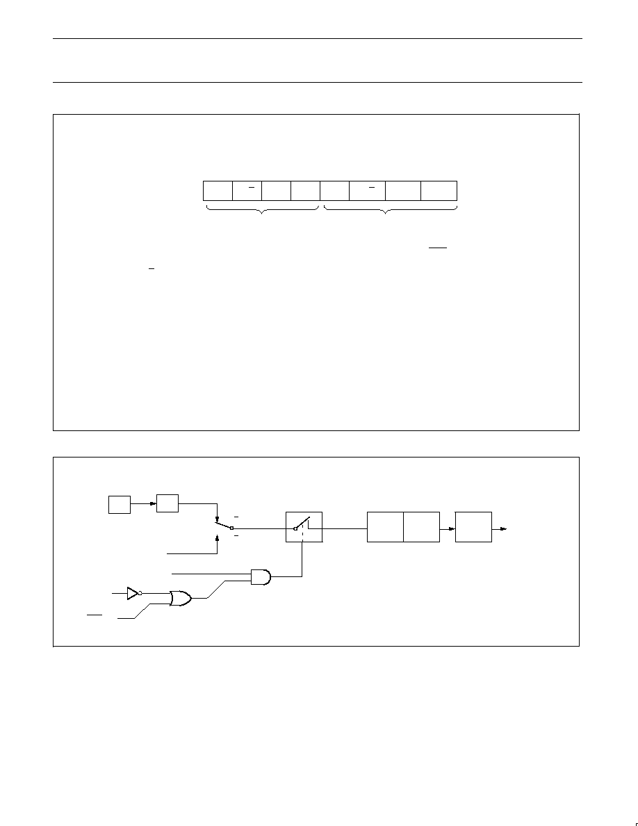
Mode 0
Putting either Timer into Mode 0 makes it look like an 8048 Timer,
which is an 8-bit Counter with a divide-by-32 prescaler. Figure 2
shows the Mode 0 operation.
In this mode, the Timer register is configured as a 13-bit register. As
the count rolls over from all 1s to all 0s, it sets the Timer interrupt
flag TFn. The counted input is enabled to the Timer when TRn = 1
and either GATE = 0 or INTn = 1. (Setting GATE = 1 allows the
Timer to be controlled by external input INTn, to facilitate pulse width
measurements). TRn is a control bit in the Special Function Register
TCON (Figure 3).
The 13-bit register consists of all 8 bits of THn and the lower 5 bits
of TLn. The upper 3 bits of TLn are indeterminate and should be
ignored. Setting the run flag (TRn) does not clear the registers.
Mode 0 operation is the same for Timer 0 as for Timer 1. There are
two different GATE bits, one for Timer 1 (TMOD.7) and one for Timer
0 (TMOD.3).
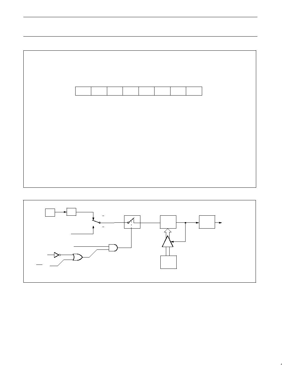
Mode 1
Mode 1 is the same as Mode 0, except that the Timer register is
being run with all 16 bits.
Mode 2
Mode 2 configures the Timer register as an 8-bit Counter (TLn) with
automatic reload, as shown in Figure 4. Overflow from TLn not only
sets TFn, but also reloads TLn with the contents of THn, which is
preset by software. The reload leaves THn unchanged.
Mode 2 operation is the same for Timer 0 as for Timer 1.
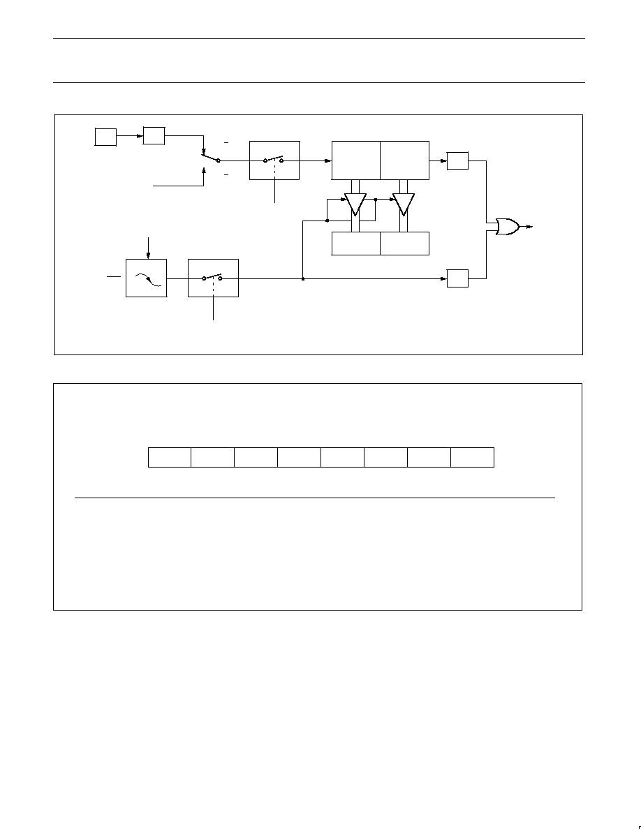
Mode 3
Timer 1 in Mode 3 simply holds its count. The effect is the same as
setting TR1 = 0.
Timer 0 in Mode 3 establishes TL0 and TH0 as two separate
counters. The logic for Mode 3 on Timer 0 is shown in Figure 5. TL0
uses the Timer 0 control bits: C/T, GATE, TR0, and TF0 as well as
pin INT0. TH0 is locked into a timer function (counting machine
cycles) and takes over the use of TR1 and TF1 from Timer 1. Thus,
TH0 now controls the "Timer 1" interrupt.
Mode 3 is provided for applications requiring an extra 8-bit timer on
the counter. With Timer 0 in Mode 3, an 80C51 can look like it has
three Timer/Counters. When Timer 0 is in Mode 3, Timer 1 can be
turned on and off by switching it out of and into its own Mode 3, or
can still be used by the serial port as a baud rate generator, or in
fact, in any application not requiring an interrupt.
Philips Semiconductors
Product data
P80C3xX2; P80C5xX2;
P87C5xX2
80C51 8-bit microcontroller family
4K/8K/16K/32K ROM/OTP, low voltage (2.7 to 5.5 V),
low power, high speed (30/33 MHz)
2003 Jan 24
15
GATE
C/T
M1
M0
GATE
C/T
M1
M0
BIT
SYMBOL
FUNCTION
TMOD.3/
GATE
Gating control when set. Timer/Counter "n" is enabled only while "INTn" pin is high and
TMOD.7
"TRn" control pin is set. when cleared Timer "n" is enabled whenever "TRn" control bit is set.
TMOD.2/
C/T
Timer or Counter Selector cleared for Timer operation (input from internal system clock.)
TMOD.6
Set for Counter operation (input from "Tn" input pin).
M1
M0
OPERATING
0
0
8048 Timer: "TLn" serves as 5-bit prescaler.
0
1
16-bit Timer/Counter: "THn" and "TLn" are cascaded; there is no prescaler.
1
0
8-bit auto-reload Timer/Counter: "THn" holds a value which is to be reloaded
into "TLn" each time it overflows.
1
1
(Timer 0) TL0 is an 8-bit Timer/Counter controlled by the standard Timer 0 control bits.
TH0 is an 8-bit timer only controlled by Timer 1 control bits.
1
1
(Timer 1) Timer/Counter 1 stopped.
SU01580
TIMER 1
TIMER 0
Not Bit Addressable
TMOD
Address = 89H
Reset Value = 00H
7
6
5
4
3
2
1
0
Figure 1. Timer/Counter 0/1 Mode Control (TMOD) Register
INTn Pin
Timer n
Gate bit
TRn
TLn
(5 Bits)
THn
(8 Bits)
TFn
Interrupt
Control
C/T = 0
C/T = 1
SU01618
OSC
˜
d*
Tn Pin
*d = 6 in 6-clock mode; d = 12 in 12-clock mode.
Figure 2. Timer/Counter 0/1 Mode 0: 13-Bit Timer/Counter
Philips Semiconductors
Product data
P80C3xX2; P80C5xX2;
P87C5xX2
80C51 8-bit microcontroller family
4K/8K/16K/32K ROM/OTP, low voltage (2.7 to 5.5 V),
low power, high speed (30/33 MHz)
2003 Jan 24
16
IT0
BIT
SYMBOL
FUNCTION
TCON.7
TF1
Timer 1 overflow flag. Set by hardware on Timer/Counter overflow.
Cleared by hardware when processor vectors to interrupt routine, or clearing the bit in software.
TCON.6
TR1
Timer 1 Run control bit. Set/cleared by software to turn Timer/Counter on/off.
TCON.5
TF0
Timer 0 overflow flag. Set by hardware on Timer/Counter overflow.
Cleared by hardware when processor vectors to interrupt routine, or by clearing the bit in software.
TCON.4
TR0
Timer 0 Run control bit. Set/cleared by software to turn Timer/Counter on/off.
TCON.3
IE1
Interrupt 1 Edge flag. Set by hardware when external interrupt edge detected.
Cleared when interrupt processed.
TCON.2
IT1
Interrupt 1 type control bit. Set/cleared by software to specify falling edge/low level triggered
external interrupts.
TCON.1
IE0
Interrupt 0 Edge flag. Set by hardware when external interrupt edge detected.
Cleared when interrupt processed.
TCON.0
IT0
Interrupt 0 Type control bit. Set/cleared by software to specify falling edge/low level
triggered external interrupts.
SU01516
IE0
IT1
IE1
TR0
TF0
TR1
TF1
Bit Addressable
TCON
Address = 88H
Reset Value = 00H
7
6
5
4
3
2
1
0
Figure 3. Timer/Counter 0/1 Control (TCON) Register
TLn
(8 Bits)
TFn
Interrupt
Control
C/T = 0
C/T = 1
THn
(8 Bits)
Reload
INTn Pin
Timer n
Gate bit
TRn
SU01619
OSC
˜
d*
Tn Pin
*d = 6 in 6-clock mode; d = 12 in 12-clock mode.
Figure 4. Timer/Counter 0/1 Mode 2: 8-Bit Auto-Reload

Philips Semiconductors
Product data
P80C3xX2; P80C5xX2;
P87C5xX2
80C51 8-bit microcontroller family
4K/8K/16K/32K ROM/OTP, low voltage (2.7 to 5.5 V),
low power, high speed (30/33 MHz)
2003 Jan 24
17
TL0
(8 Bits)
TF0
Interrupt
Control
TH0
(8 Bits)
TF1
Interrupt
Control
TR1
INT0 Pin
Timer 0
Gate bit
TR0
SU01620
C/T = 0
C/T = 1
*d = 6 in 6-clock mode; d = 12 in 12-clock mode.
OSC
˜
d*
OSC
˜
d*
T0 Pin
Figure 5. Timer/Counter 0 Mode 3: Two 8-Bit Counters
TIMER 2 OPERATION
Timer 2
Timer 2 is a 16-bit Timer/Counter which can operate as either an
event timer or an event counter, as selected by C/T2 in the special
function register T2CON (see Figure 6). Timer 2 has three operating
modes: Capture, Auto-reload (up or down counting), and Baud Rate
Generator, which are selected by bits in the T2CON as shown in
Table 4.
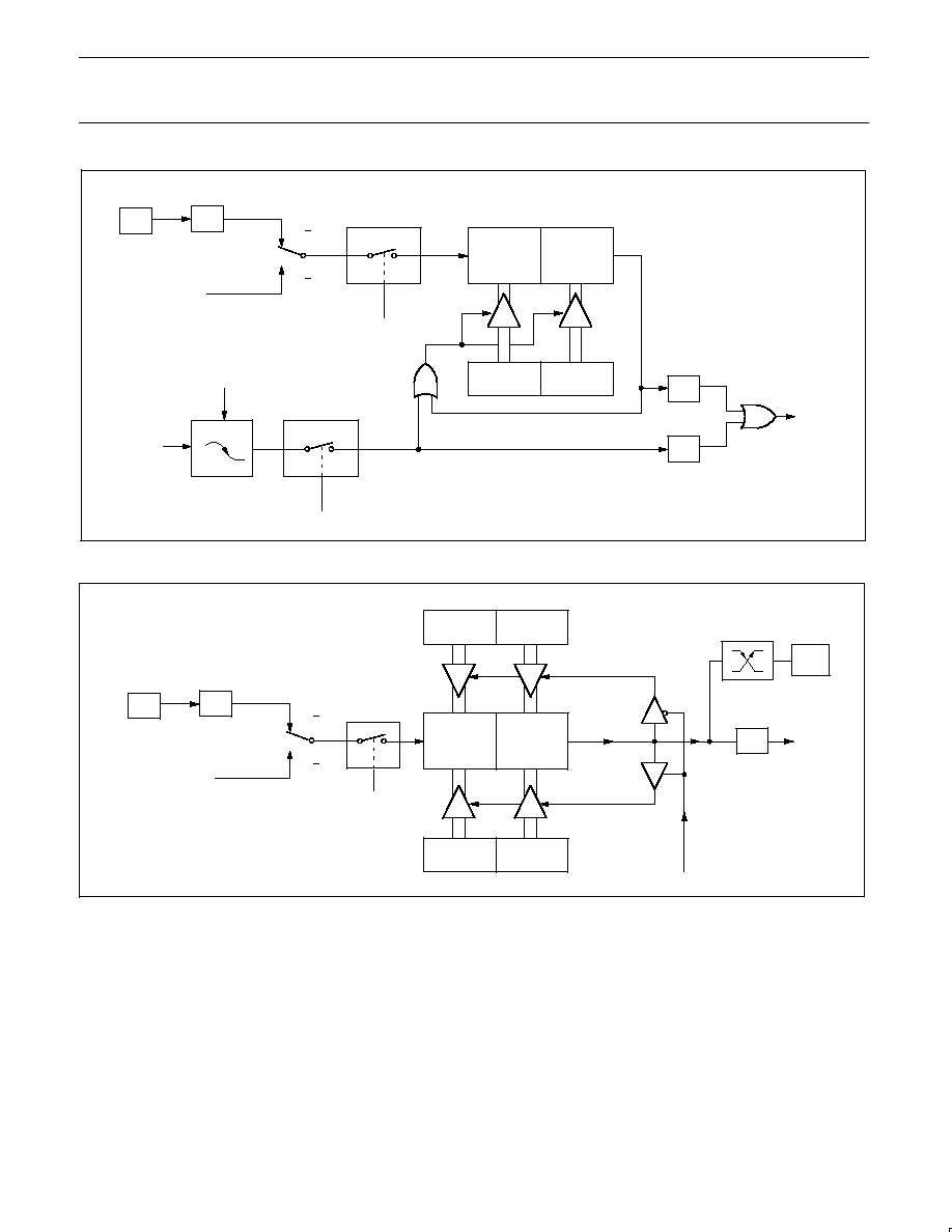
Capture Mode
In the capture mode there are two options which are selected by bit
EXEN2 in T2CON. If EXEN2=0, then timer 2 is a 16-bit timer or
counter (as selected by C/T2 in T2CON) which, upon overflowing,
sets bit TF2, the timer 2 overflow bit. This bit can be used to
generate an interrupt (by enabling the Timer 2 interrupt bit in the
IE register). If EXEN2=1, Timer 2 operates as described above, but
with the added feature that a 1-to-0 transition at external input T2EX
causes the current value in the Timer 2 registers, TL2 and TH2, to
be captured into registers RCAP2L and RCAP2H, respectively. In
addition, the transition at T2EX causes bit EXF2 in T2CON to be
set, and EXF2 (like TF2) can generate an interrupt (which vectors to
the same location as Timer 2 overflow interrupt. The Timer 2
interrupt service routine can interrogate TF2 and EXF2 to determine
which event caused the interrupt). The capture mode is illustrated in
Figure 7 (There is no reload value for TL2 and TH2 in this mode.
Even when a capture event occurs from T2EX, the counter keeps on
counting T2EX pin transitions or osc/12 (12-clock Mode) or osc/6
(6-clock Mode) pulses).
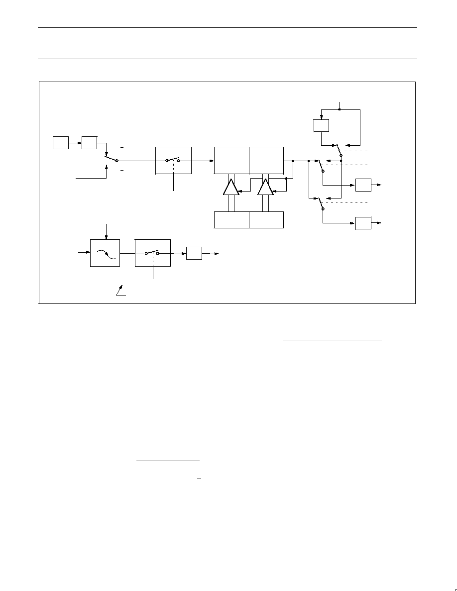
Auto-Reload Mode (Up or Down Counter)
In the 16-bit auto-reload mode, Timer 2 can be configured as either
a timer or counter (C/T2 in T2CON), then programmed to count up
or down. The counting direction is determined by bit DCEN (Down
Counter Enable) which is located in the T2MOD register (see
Figure 8). After reset, DCEN=0 which means Timer 2 will default to
counting up. If DCEN is set, Timer 2 can count up or down
depending on the value of the T2EX pin.
Figure 9 shows Timer 2 which will count up automatically since
DCEN=0. In this mode there are two options selected by bit EXEN2
in T2CON register. If EXEN2=0, then Timer 2 counts up to 0FFFFH
and sets the TF2 (Overflow Flag) bit upon overflow. This causes the
Timer 2 registers to be reloaded with the 16-bit value in RCAP2L
and RCAP2H. The values in RCAP2L and RCAP2H are preset by
software.
If EXEN2=1, then a 16-bit reload can be triggered either by an
overflow or by a 1-to-0 transition at input T2EX. This transition also
sets the EXF2 bit. The Timer 2 interrupt, if enabled, can be
generated when either TF2 or EXF2 are 1.
In Figure 10 DCEN=1 which enables Timer 2 to count up or down.
This mode allows pin T2EX to control the direction of count. When a
logic 1 is applied at pin T2EX, Timer 2 will count up. Timer 2 will
overflow at 0FFFFH and set the TF2 flag, which can then generate
an interrupt, if the interrupt is enabled. This timer overflow also
causes the 16-bit value in RCAP2L and RCAP2H to be reloaded
into the timer registers TL2 and TH2.
A logic 0 applied to pin T2EX causes Timer 2 to count down. The
timer will underflow when TL2 and TH2 become equal to the value
stored in RCAP2L and RCAP2H. A Timer 2 underflow sets the TF2
flag and causes 0FFFFH to be reloaded into the timer registers TL2
and TH2.
The external flag EXF2 toggles when Timer 2 underflows or
overflows. This EXF2 bit can be used as a 17th bit of resolution if
needed. The EXF2 flag does not generate an interrupt in this mode
of operation.
Philips Semiconductors
Product data
P80C3xX2; P80C5xX2;
P87C5xX2
80C51 8-bit microcontroller family
4K/8K/16K/32K ROM/OTP, low voltage (2.7 to 5.5 V),
low power, high speed (30/33 MHz)
2003 Jan 24
18
Table 4. Timer 2 Operating Modes
RCLK + TCLK
CP/RL2
TR2
MODE
0
0
1
16-bit Auto-reload
0
1
1
16-bit Capture
1
X
1
Baud rate generator
X
X
0
(off)
Symbol
Position
Name and Significance
TF2
T2CON.7
Timer 2 overflow flag set by a Timer 2 overflow and must be cleared by software. TF2 will not be set
when either RCLK or TCLK = 1.
EXF2
T2CON.6
Timer 2 external flag set when either a capture or reload is caused by a negative transition on T2EX and
EXEN2 = 1. When Timer 2 interrupt is enabled, EXF2 = 1 will cause the CPU to vector to the Timer 2
interrupt routine. EXF2 must be cleared by software. EXF2 does not cause an interrupt in up/down
counter mode (DCEN = 1).
RCLK
T2CON.5
Receive clock flag. When set, causes the serial port to use Timer 2 overflow pulses for its receive clock
in modes 1 and 3. RCLK = 0 causes Timer 1 overflow to be used for the receive clock.
TCLK
T2CON.4
Transmit clock flag. When set, causes the serial port to use Timer 2 overflow pulses for its transmit clock
in modes 1 and 3. TCLK = 0 causes Timer 1 overflows to be used for the transmit clock.
EXEN2
T2CON.3
Timer 2 external enable flag. When set, allows a capture or reload to occur as a result of a negative
transition on T2EX if Timer 2 is not being used to clock the serial port. EXEN2 = 0 causes Timer 2 to
ignore events at T2EX.
TR2
T2CON.2
Start/stop control for Timer 2. A logic 1 starts the timer.
C/T2
T2CON.1
Timer or counter select. (Timer 2)
0 = Internal timer (OSC/12 in 12-clock mode or OSC/6 in 6-clock mode)
1 = External event counter (falling edge triggered).
CP/RL2
T2CON.0
Capture/Reload flag. When set, captures will occur on negative transitions at T2EX if EXEN2 = 1. When
cleared, auto-reloads will occur either with Timer 2 overflows or negative transitions at T2EX when
EXEN2 = 1. When either RCLK = 1 or TCLK = 1, this bit is ignored and the timer is forced to auto-reload
on Timer 2 overflow.
TF2
EXF2
RCLK
TCLK
EXEN2
TR2
C/T2
CP/RL2
SU01621
Bit Addressable
T2CON
Address = C8H
Reset Value = 00H
7
6
5
4
3
2
1
0
Figure 6. Timer/Counter 2 (T2CON) Control Register
Philips Semiconductors
Product data
P80C3xX2; P80C5xX2;
P87C5xX2
80C51 8-bit microcontroller family
4K/8K/16K/32K ROM/OTP, low voltage (2.7 to 5.5 V),
low power, high speed (30/33 MHz)
2003 Jan 24
19
TR2
Control
TL2
(8 bits)
TH2
(8 bits)
TF2
RCAP2L
RCAP2H
EXEN2
Control
EXF2
Timer 2
Interrupt
T2EX Pin
Transition
Detector
Capture
SU01622
C/T2 = 0
C/T2 = 1
*n = 6 in 6-clock mode; n = 12 in 12-clock mode.
OSC
˜
n*
T2 Pin
Figure 7. Timer 2 in Capture Mode
Not Bit Addressable
Symbol
Position
Function
--
Not implemented, reserved for future use.*
T2OE
T2MOD.1
Timer 2 Output Enable bit.
DCEN
T2MOD.0
Down Count Enable bit. When set, this allows Timer 2 to be configured as an up/down
counter.
--
--
--
--
--
--
T2OE
DCEN
SU01519
7
6
5
4
3
2
1
0
*
User software should not write 1s to reserved bits. These bits may be used in future 8051 family products to invoke new features.
In that case, the reset or inactive value of the new bit will be 0, and its active value will be 1. The value read from a reserved bit is
indeterminate.
T2MOD
Address = 0C9H
Reset Value = XXXX XX00B
Figure 8. Timer 2 Mode (T2MOD) Control Register
Philips Semiconductors
Product data
P80C3xX2; P80C5xX2;
P87C5xX2
80C51 8-bit microcontroller family
4K/8K/16K/32K ROM/OTP, low voltage (2.7 to 5.5 V),
low power, high speed (30/33 MHz)
2003 Jan 24
20
TR2
CONTROL
TL2
(8-BITS)
TH2
(8-BITS)
TF2
RCAP2L
RCAP2H
EXEN2
CONTROL
EXF2
TIMER 2
INTERRUPT
T2EX PIN
TRANSITION
DETECTOR
RELOAD
SU01623
C/T2 = 0
C/T2 = 1
*n = 6 in 6-clock mode; n = 12 in 12-clock mode.
OSC
˜
n*
T2 Pin
Figure 9. Timer 2 in Auto-Reload Mode (DCEN = 0)
TL2
TH2
TR2
CONTROL
SU01624
FFH
FFH
RCAP2L
RCAP2H
(UP COUNTING RELOAD VALUE)
T2EX PIN
TF2
INTERRUPT
COUNT
DIRECTION
1 = UP
0 = DOWN
EXF2
OVERFLOW
(DOWN COUNTING RELOAD VALUE)
TOGGLE
C/T2 = 0
C/T2 = 1
*n = 6 in 6-clock mode; n = 12 in 12-clock mode.
OSC
˜
n*
T2 Pin
Figure 10. Timer 2 Auto Reload Mode (DCEN = 1)
Philips Semiconductors
Product data
P80C3xX2; P80C5xX2;
P87C5xX2
80C51 8-bit microcontroller family
4K/8K/16K/32K ROM/OTP, low voltage (2.7 to 5.5 V),
low power, high speed (30/33 MHz)
2003 Jan 24
21
OSC
˜
n
C/T2 = 0
C/T2 = 1
TR2
Control
TL2
(8 bits)
TH2
(8 bits)
˜
16
RCAP2L
RCAP2H
EXEN2
Control
EXF2
Timer 2
Interrupt
T2EX Pin
Transition
Detector
T2 Pin
Reload
˜
2
"0"
"1"
RX Clock
˜
16
TX Clock
"0"
"1"
"0"
"1"
Timer 1
Overflow
Note availability of additional external interrupt.
SMOD
RCLK
TCLK
SU01625
n = 1 in 6-clock mode
n = 2 in 12-clock mode.
Figure 11. Timer 2 in Baud Rate Generator Mode
Baud Rate Generator Mode
Bits TCLK and/or RCLK in T2CON (Table 4) allow the serial port
transmit and receive baud rates to be derived from either Timer 1 or
Timer 2. When TCLK= 0, Timer 1 is used as the serial port transmit
baud rate generator. When TCLK= 1, Timer 2 is used as the serial
port transmit baud rate generator. RCLK has the same effect for the
serial port receive baud rate. With these two bits, the serial port can
have different receive and transmit baud rates ≠ one generated by
Timer 1, the other by Timer 2.
Figure 11 shows the Timer 2 in baud rate generation mode. The
baud rate generation mode is like the auto-reload mode, in that a
rollover in TH2 causes the Timer 2 registers to be reloaded with the
16-bit value in registers RCAP2H and RCAP2L, which are preset by
software.
The baud rates in modes 1 and 3 are determined by Timer 2's
overflow rate given below:
Modes 1 and 3 Baud Rates
+
Timer 2 Overflow Rate
16
The timer can be configured for either "timer" or "counter" operation.
In many applications, it is configured for "timer" operation (C/T2=0).
Timer operation is different for Timer 2 when it is being used as a
baud rate generator.
Usually, as a timer it would increment every machine cycle (i.e., 1/6
the oscillator frequency in 6-clock mode or 1/12 the oscillator
frequency in 12-clock mode). As a baud rate generator, it
increments at the oscillator frequency in 6-clock mode or at 1/2 the
oscillator frequency in 12-clock mode. Thus the baud rate formula is
as follows:
Oscillator Frequency
[n
[65536
*
(RCAP2H, RCAP2L)]]
Modes 1 and 3 Baud Rates =
Where:
n = 16 in 6-clock mode, 32 in 12-clock mode.
(RCAP2H, RCAP2L)= The content of RCAP2H and RCAP2L
taken as a 16-bit unsigned integer.
The Timer 2 as a baud rate generator mode shown in Figure 11 is
valid only if RCLK and/or TCLK = 1 in T2CON register. Note that a
rollover in TH2 does not set TF2, and will not generate an interrupt.
Thus, the Timer 2 interrupt does not have to be disabled when
Timer 2 is in the baud rate generator mode. Also if the EXEN2
(T2 external enable flag) is set, a 1-to-0 transition in T2EX
(Timer/counter 2 trigger input) will set EXF2 (T2 external flag) but
will not cause a reload from (RCAP2H, RCAP2L) to (TH2,TL2).
Therefore when Timer 2 is in use as a baud rate generator, T2EX
can be used as an additional external interrupt, if needed.
When Timer 2 is in the baud rate generator mode, one should not try
to read or write TH2 and TL2. As a baud rate generator, Timer 2 is
incremented every state time (osc/2) or asynchronously from pin T2;
under these conditions, a read or write of TH2 or TL2 may not be
accurate. The RCAP2 registers may be read, but should not be
written to, because a write might overlap a reload and cause write
and/or reload errors. The timer should be turned off (clear TR2)
before accessing the Timer 2 or RCAP2 registers.
Table 5 shows commonly used baud rates and how they can be
obtained from Timer 2.
Philips Semiconductors
Product data
P80C3xX2; P80C5xX2;
P87C5xX2
80C51 8-bit microcontroller family
4K/8K/16K/32K ROM/OTP, low voltage (2.7 to 5.5 V),
low power, high speed (30/33 MHz)
2003 Jan 24
22
Table 5. Timer 2 Generated Commonly Used
Baud Rates
Baud Rate
Timer 2
12-clk
mode
6-clk
mode
Osc Freq
RCAP2H
RCAP2L
375 K
750 K
12 MHz
FF
FF
9.6 K
19.2 K
12 MHz
FF
D9
4.8 K
9.6 K
12 MHz
FF
B2
2.4 K
4.8 K
12 MHz
FF
64
1.2 K
2.4 K
12 MHz
FE
C8
300
600
12 MHz
FB
1E
110
220
12 MHz
F2
AF
300
600
6 MHz
FD
8F
110
220
6 MHz
F9
57
Summary Of Baud Rate Equations
Timer 2 is in baud rate generating mode. If Timer 2 is being clocked
through pin T2(P1.0) the baud rate is:
Baud Rate
+
Timer 2 Overflow Rate
16
If Timer 2 is being clocked internally, the baud rate is:
Baud Rate
+
f
OSC
[n
[65536
*
(RCAP2H, RCAP2L)]]
Where:
n = 16 in 6-clock mode, 32 in 12-clock mode.
f
OSC
= Oscillator Frequency
To obtain the reload value for RCAP2H and RCAP2L, the above
equation can be rewritten as:
RCAP2H, RCAP2L
+
65536
*
f
OSC
n
Baud Rate
Timer/Counter 2 Set-up
Except for the baud rate generator mode, the values given for
T2CON do not include the setting of the TR2 bit. Therefore, bit TR2
must be set, separately, to turn the timer on. See Table 6 for set-up
of Timer 2 as a timer. Also see Table 7 for set-up of Timer 2 as a
counter.
Table 6. Timer 2 as a Timer
T2CON
MODE
INTERNAL
CONTROL
(Note 1)
EXTERNAL
CONTROL
(Note 2)
16-bit Auto-Reload
00H
08H
16-bit Capture
01H
09H
Baud rate generator receive
and transmit same baud rate
34H
36H
Receive only
24H
26H
Transmit only
14H
16H
Table 7. Timer 2 as a Counter
TMOD
MODE
INTERNAL
CONTROL
(Note 1)
EXTERNAL
CONTROL
(Note 2)
16-bit
02H
0AH
Auto-Reload
03H
0BH
NOTES:
1. Capture/reload occurs only on timer/counter overflow.
2. Capture/reload occurs on timer/counter overflow and a 1-to-0
transition on T2EX (P1.1) pin except when Timer 2 is used in the
baud rate generator mode.

Philips Semiconductors
Product data
P80C3xX2; P80C5xX2;
P87C5xX2
80C51 8-bit microcontroller family
4K/8K/16K/32K ROM/OTP, low voltage (2.7 to 5.5 V),
low power, high speed (30/33 MHz)
2003 Jan 24
23
FULL-DUPLEX ENHANCED UART
Standard UART operation
The serial port is full duplex, meaning it can transmit and receive
simultaneously. It is also receive-buffered, meaning it can
commence reception of a second byte before a previously received
byte has been read from the register. (However, if the first byte still
hasn't been read by the time reception of the second byte is
complete, one of the bytes will be lost.) The serial port receive and
transmit registers are both accessed at Special Function Register
SBUF. Writing to SBUF loads the transmit register, and reading
SBUF accesses a physically separate receive register.
The serial port can operate in 4 modes:
Mode 0:
Serial data enters and exits through RxD. TxD outputs
the shift clock. 8 bits are transmitted/received (LSB first).
The baud rate is fixed at 1/12 the oscillator frequency in
12-clock mode or 1/6 the oscillator frequency in 6-clock
mode.
Mode 1:
10 bits are transmitted (through TxD) or received
(through RxD): a start bit (0), 8 data bits (LSB first), and
a stop bit (1). On receive, the stop bit goes into RB8 in
Special Function Register SCON. The baud rate is
variable.
Mode 2:
11 bits are transmitted (through TxD) or received
(through RxD): start bit (0), 8 data bits (LSB first), a
programmable 9th data bit, and a stop bit (1). On
Transmit, the 9th data bit (TB8 in SCON) can be
assigned the value of 0 or 1. Or, for example, the parity
bit (P, in the PSW) could be moved into TB8. On receive,
the 9th data bit goes into RB8 in Special Function
Register SCON, while the stop bit is ignored. The baud
rate is programmable to either 1/32 or 1/64 the oscillator
frequency in 12-clock mode or 1/16 or 1/32 the oscillator
frequency in 6-clock mode.
Mode 3:
11 bits are transmitted (through TxD) or received
(through RxD): a start bit (0), 8 data bits (LSB first), a
programmable 9th data bit, and a stop bit (1). In fact,
Mode 3 is the same as Mode 2 in all respects except
baud rate. The baud rate in Mode 3 is variable.
In all four modes, transmission is initiated by any instruction that
uses SBUF as a destination register. Reception is initiated in Mode 0
by the condition RI = 0 and REN = 1. Reception is initiated in the
other modes by the incoming start bit if REN = 1.
Multiprocessor Communications
Modes 2 and 3 have a special provision for multiprocessor
communications. In these modes, 9 data bits are received. The 9th
one goes into RB8. Then comes a stop bit. The port can be
programmed such that when the stop bit is received, the serial port
interrupt will be activated only if RB8 = 1. This feature is enabled by
setting bit SM2 in SCON. A way to use this feature in multiprocessor
systems is as follows:
When the master processor wants to transmit a block of data to one
of several slaves, it first sends out an address byte which identifies
the target slave. An address byte differs from a data byte in that the
9th bit is 1 in an address byte and 0 in a data byte. With SM2 = 1, no
slave will be interrupted by a data byte. An address byte, however,
will interrupt all slaves, so that each slave can examine the received
byte and see if it is being addressed. The addressed slave will clear
its SM2 bit and prepare to receive the data bytes that will be coming.
The slaves that weren't being addressed leave their SM2s set and
go on about their business, ignoring the coming data bytes.
SM2 has no effect in Mode 0, and in Mode 1 can be used to check
the validity of the stop bit. In a Mode 1 reception, if SM2 = 1, the
receive interrupt will not be activated unless a valid stop bit is
received.
Serial Port Control Register
The serial port control and status register is the Special Function
Register SCON, shown in Figure 12. This register contains not only
the mode selection bits, but also the 9th data bit for transmit and
receive (TB8 and RB8), and the serial port interrupt bits (TI and RI).
Baud Rates
The baud rate in Mode 0 is fixed: Mode 0 Baud Rate = Oscillator
Frequency / 12 (12-clock mode) or / 6 (6-clock mode). The baud
rate in Mode 2 depends on the value of bit SMOD in Special
Function Register PCON. If SMOD = 0 (which is the value on reset),
and the port pins in 12-clock mode, the baud rate is 1/64 the
oscillator frequency. If SMOD = 1, the baud rate is 1/32 the oscillator
frequency. In 6-clock mode, the baud rate is 1/32 or 1/16 the
oscillator frequency, respectively.
Mode 2 Baud Rate =
2
SMOD
n
(Oscillator Frequency)
Where:
n = 64 in 12-clock mode, 32 in 6-clock mode
The baud rates in Modes 1 and 3 are determined by the Timer 1 or
Timer 2 overflow rate.
Using Timer 1 to Generate Baud Rates
When Timer 1 is used as the baud rate generator (T2CON.RCLK
= 0, T2CON.TCLK = 0), the baud rates in Modes 1 and 3 are
determined by the Timer 1 overflow rate and the value of SMOD as
follows:
Mode 1, 3 Baud Rate =
2
SMOD
n
(Timer 1 Overflow Rate)
Where:
n = 32 in 12-clock mode, 16 in 6-clock mode
The Timer 1 interrupt should be disabled in this application. The
Timer itself can be configured for either "timer" or "counter"
operation, and in any of its 3 running modes. In the most typical
applications, it is configured for "timer" operation, in the auto-reload
mode (high nibble of TMOD = 0010B). In that case the baud rate is
given by the formula:
Mode 1, 3 Baud Rate =
2
SMOD
n
Oscillator Frequency
12
[256≠(TH1)]
Where:
n = 32 in 12-clock mode, 16 in 6-clock mode
One can achieve very low baud rates with Timer 1 by leaving the
Timer 1 interrupt enabled, and configuring the Timer to run as a
16-bit timer (high nibble of TMOD = 0001B), and using the Timer 1
interrupt to do a 16-bit software reload. Figure 13 lists various
commonly used baud rates and how they can be obtained from
Timer 1.

Philips Semiconductors
Product data
P80C3xX2; P80C5xX2;
P87C5xX2
80C51 8-bit microcontroller family
4K/8K/16K/32K ROM/OTP, low voltage (2.7 to 5.5 V),
low power, high speed (30/33 MHz)
2003 Jan 24
24
SM2
Enables the multiprocessor communication feature in Modes 2 and 3. In Mode 2 or 3, if SM2 is set to 1, then Rl will not be
activated if the received 9th data bit (RB8) is 0. In Mode 1, if SM2=1 then RI will not be activated if a valid stop bit was not
received. In Mode 0, SM2 should be 0.
REN
Enables serial reception. Set by software to enable reception. Clear by software to disable reception.
TB8
The 9th data bit that will be transmitted in Modes 2 and 3. Set or clear by software as desired.
RB8
In Modes 2 and 3, is the 9th data bit that was received. In Mode 1, it SM2=0, RB8 is the stop bit that was received. In Mode 0,
RB8 is not used.
TI
Transmit interrupt flag. Set by hardware at the end of the 8th bit time in Mode 0, or at the beginning of the stop bit in the other
modes, in any serial transmission. Must be cleared by software.
RI
Receive interrupt flag. Set by hardware at the end of the 8th bit time in Mode 0, or halfway through the stop bit time in the other
modes, in any serial reception (except see SM2). Must be cleared by software.
SM0
SM1
SM2
REN
TB8
RB8
TI
RI
Where SM0, SM1 specify the serial port mode, as follows:
SM0
SM1
Mode
Description
Baud Rate
0
0
0
shift register
f
OSC
/12 (12-clock mode) or f
OSC
/6 (6-clock mode)
0
1
1
8-bit UART
variable
1
0
2
9-bit UART
f
OSC
/64 or f
OSC
/32 (12-clock mode) or f
OSC
/32 or f
OSC
/16 (6-clock mode)
1
1
3 9-bit
UART
variable
SU01626
Bit Addressable
SCON
Address = 98H
Reset Value = 00H
7
6
5
4
3
2
1
0
Figure 12. Serial Port Control (SCON) Register
Baud Rate
f
SMOD
Timer 1
Mode
12-clock mode
6-clock mode
f
OSC
SMOD
C/T
Mode
Reload Value
Mode 0 Max
1.67 MHz
3.34 MHz
20 MHz
X
X
X
X
Mode 2 Max
625 k
1250 k
20 MHz
1
X
X
X
Mode 1, 3 Max
104.2 k
208.4 k
20 MHz
1
0
2
FFH
Mode 1, 3
19.2 k
38.4 k
11.059 MHz
1
0
2
FDH
9.6 k
19.2 k
11.059 MHz
0
0
2
FDH
4.8 k
9.6 k
11.059 MHz
0
0
2
FAH
2.4 k
4.8 k
11.059 MHz
0
0
2
F4H
1.2 k
2.4 k
11.059 MHz
0
0
2
E8H
137.5
275
11.986 MHz
0
0
2
1DH
110
220
6 MHz
0
0
2
72H
110
220
12 MHz
0
0
1
FEEBH
Figure 13. Timer 1 Generated Commonly Used Baud Rates
More About Mode 0
Serial data enters and exits through RxD. TxD outputs the shift
clock. 8 bits are transmitted/received: 8 data bits (LSB first). The
baud rate is fixed a 1/12 the oscillator frequency (12-clock mode) or
1/6 the oscillator frequency (6-clock mode).
Figure 14 shows a simplified functional diagram of the serial port in
Mode 0, and associated timing.
Transmission is initiated by any instruction that uses SBUF as a
destination register. The "write to SBUF" signal at S6P2 also loads a
1 into the 9th position of the transmit shift register and tells the TX
Control block to commence a transmission. The internal timing is
such that one full machine cycle will elapse between "write to SBUF"
and activation of SEND.
SEND enables the output of the shift register to the alternate output
function line of P3.0 and also enable SHIFT CLOCK to the alternate
output function line of P3.1. SHIFT CLOCK is low during S3, S4, and
S5 of every machine cycle, and high during S6, S1, and S2. At
S6P2 of every machine cycle in which SEND is active, the contents
of the transmit shift are shifted to the right one position.
As data bits shift out to the right, zeros come in from the left. When
the MSB of the data byte is at the output position of the shift register,
then the 1 that was initially loaded into the 9th position, is just to the
left of the MSB, and all positions to the left of that contain zeros.
This condition flags the TX Control block to do one last shift and
then deactivate SEND and set T1. Both of these actions occur at
S1P1 of the 10th machine cycle after "write to SBUF."
Reception is initiated by the condition REN = 1 and R1 = 0. At S6P2
of the next machine cycle, the RX Control unit writes the bits
11111110 to the receive shift register, and in the next clock phase
activates RECEIVE.
RECEIVE enable SHIFT CLOCK to the alternate output function line
of P3.1. SHIFT CLOCK makes transitions at S3P1 and S6P1 of
every machine cycle. At S6P2 of every machine cycle in which
RECEIVE is active, the contents of the receive shift register are

Philips Semiconductors
Product data
P80C3xX2; P80C5xX2;
P87C5xX2
80C51 8-bit microcontroller family
4K/8K/16K/32K ROM/OTP, low voltage (2.7 to 5.5 V),
low power, high speed (30/33 MHz)
2003 Jan 24
25
shifted to the left one position. The value that comes in from the right
is the value that was sampled at the P3.0 pin at S5P2 of the same
machine cycle.
As data bits come in from the right, 1s shift out to the left. When the
0 that was initially loaded into the rightmost position arrives at the
leftmost position in the shift register, it flags the RX Control block to
do one last shift and load SBUF. At S1P1 of the 10th machine cycle
after the write to SCON that cleared RI, RECEIVE is cleared as RI is
set.
More About Mode 1
Ten bits are transmitted (through TxD), or received (through RxD): a
start bit (0), 8 data bits (LSB first), and a stop bit (1). On receive, the
stop bit goes into RB8 in SCON. In the 80C51 the baud rate is
determined by the Timer 1 or Timer 2 overflow rate.
Figure 15 shows a simplified functional diagram of the serial port in
Mode 1, and associated timings for transmit receive.
Transmission is initiated by any instruction that uses SBUF as a
destination register. The "write to SBUF" signal also loads a 1 into
the 9th bit position of the transmit shift register and flags the TX
Control unit that a transmission is requested. Transmission actually
commences at S1P1 of the machine cycle following the next rollover
in the divide-by-16 counter. (Thus, the bit times are synchronized to
the divide-by-16 counter, not to the "write to SBUF" signal.)
The transmission begins with activation of SEND which puts the
start bit at TxD. One bit time later, DATA is activated, which enables
the output bit of the transmit shift register to TxD. The first shift pulse
occurs one bit time after that.
As data bits shift out to the right, zeros are clocked in from the left.
When the MSB of the data byte is at the output position of the shift
register, then the 1 that was initially loaded into the 9th position is
just to the left of the MSB, and all positions to the left of that contain
zeros. This condition flags the TX Control unit to do one last shift
and then deactivate SEND and set TI. This occurs at the 10th
divide-by-16 rollover after "write to SBUF."
Reception is initiated by a detected 1-to-0 transition at RxD. For this
purpose RxD is sampled at a rate of 16 times whatever baud rate
has been established. When a transition is detected, the
divide-by-16 counter is immediately reset, and 1FFH is written into
the input shift register. Resetting the divide-by-16 counter aligns its
rollovers with the boundaries of the incoming bit times.
The 16 states of the counter divide each bit time into 16ths. At the
7th, 8th, and 9th counter states of each bit time, the bit detector
samples the value of RxD. The value accepted is the value that was
seen in at least 2 of the 3 samples. This is done for noise rejection.
If the value accepted during the first bit time is not 0, the receive
circuits are reset and the unit goes back to looking for another 1-to-0
transition. This is to provide rejection of false start bits. If the start bit
proves valid, it is shifted into the input shift register, and reception of
the rest of the frame will proceed.
As data bits come in from the right, 1s shift out to the left. When the
start bit arrives at the leftmost position in the shift register (which in
mode 1 is a 9-bit register), it flags the RX Control block to do one
last shift, load SBUF and RB8, and set RI. The signal to load SBUF
and RB8, and to set RI, will be generated if, and only if, the following
conditions are met at the time the final shift pulse is generated.:
1. R1 = 0, and
2. Either SM2 = 0, or the received stop bit = 1.
If either of these two conditions is not met, the received frame is
irretrievably lost. If both conditions are met, the stop bit goes into
RB8, the 8 data bits go into SBUF, and RI is activated. At this time,
whether the above conditions are met or not, the unit goes back to
looking for a 1-to-0 transition in RxD.
More About Modes 2 and 3
Eleven bits are transmitted (through TxD), or received (through
RxD): a start bit (0), 8 data bits (LSB first), a programmable 9th data
bit, and a stop bit (1). On transmit, the 9th data bit (TB8) can be
assigned the value of 0 or 1. On receive, the 9the data bit goes into
RB8 in SCON. The baud rate is programmable to either 1/32 or 1/64
(12-clock mode) or 1/16 or 1/32 the oscillator frequency (6-clock
mode) the oscillator frequency in Mode 2. Mode 3 may have a
variable baud rate generated from Timer 1 or Timer 2.
Figures 16 and 17 show a functional diagram of the serial port in
Modes 2 and 3. The receive portion is exactly the same as in Mode
1. The transmit portion differs from Mode 1 only in the 9th bit of the
transmit shift register.
Transmission is initiated by any instruction that uses SBUF as a
destination register. The "write to SBUF" signal also loads TB8 into
the 9th bit position of the transmit shift register and flags the TX
Control unit that a transmission is requested. Transmission
commences at S1P1 of the machine cycle following the next rollover
in the divide-by-16 counter. (Thus, the bit times are synchronized to
the divide-by-16 counter, not to the "write to SBUF" signal.)
The transmission begins with activation of SEND, which puts the
start bit at TxD. One bit time later, DATA is activated, which enables
the output bit of the transmit shift register to TxD. The first shift pulse
occurs one bit time after that. The first shift clocks a 1 (the stop bit)
into the 9th bit position of the shift register. Thereafter, only zeros
are clocked in. Thus, as data bits shift out to the right, zeros are
clocked in from the left. When TB8 is at the output position of the
shift register, then the stop bit is just to the left of TB8, and all
positions to the left of that contain zeros. This condition flags the TX
Control unit to do one last shift and then deactivate SEND and set
TI. This occurs at the 11th divide-by-16 rollover after "write to SUBF."
Reception is initiated by a detected 1-to-0 transition at RxD. For this
purpose RxD is sampled at a rate of 16 times whatever baud rate
has been established. When a transition is detected, the
divide-by-16 counter is immediately reset, and 1FFH is written to the
input shift register.
At the 7th, 8th, and 9th counter states of each bit time, the bit
detector samples the value of R-D. The value accepted is the value
that was seen in at least 2 of the 3 samples. If the value accepted
during the first bit time is not 0, the receive circuits are reset and the
unit goes back to looking for another 1-to-0 transition. If the start bit
proves valid, it is shifted into the input shift register, and reception of
the rest of the frame will proceed.
As data bits come in from the right, 1s shift out to the left. When the
start bit arrives at the leftmost position in the shift register (which in
Modes 2 and 3 is a 9-bit register), it flags the RX Control block to do
one last shift, load SBUF and RB8, and set RI.
The signal to load SBUF and RB8, and to set RI, will be generated
if, and only if, the following conditions are met at the time the final
shift pulse is generated.
1. RI = 0, and
2. Either SM2 = 0, or the received 9th data bit = 1.
If either of these conditions is not met, the received frame is
irretrievably lost, and RI is not set. If both conditions are met, the
received 9th data bit goes into RB8, and the first 8 data bits go into
SBUF. One bit time later, whether the above conditions were met or
not, the unit goes back to looking for a 1-to-0 transition at the RxD
input.
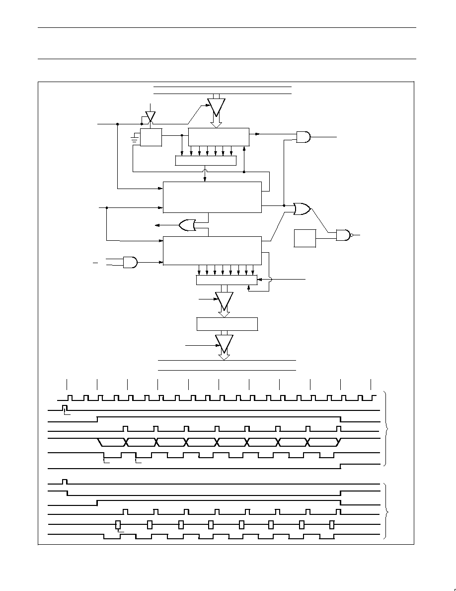
Philips Semiconductors
Product data
P80C3xX2; P80C5xX2;
P87C5xX2
80C51 8-bit microcontroller family
4K/8K/16K/32K ROM/OTP, low voltage (2.7 to 5.5 V),
low power, high speed (30/33 MHz)
2003 Jan 24
26
80C51 Internal Bus
SBUF
Zero Detector
D Q
S
CL
Write
to
SBUF
TX Control
TX Clock
Send
Shift
Start
S6
RX Control
Start
Shift
Receive
RX Clock
T1
R1
Serial
Port
Interrupt
1 1 1 1 1 1 1 0
Input Shift Register
REN
RI
Load
SBUF
Shift
Shift
Clock
RxD
P3.0 Alt
Output
Function
TxD
P3.1 Alt
Output
Function
SBUF
Read
SBUF
80C51 Internal Bus
RxD
P3.0 Alt
Input
Function
Write to SBUF
S6P2
Send
Shift
RxD (Data Out)
D0
D1
D2
D3
D4
D5
D6
D7
Transmit
TxD (Shift Clock)
TI
S3P1
S6P1
Write to SCON (Clear RI)
RI
Receive
Shift
RxD (Data In)
D0
D1
D2
D3
D4
D5
D6
TxD (Shift Clock)
S5P2
Receive
D7
ALE
S4 . .
S1
S6
. . . .
S1
S6
. . . .
S1
S6
. . . .
S1
S6
. . . .
S1
S6
. . . .
S1
S6
. . . .
S1
S6
. . . .
S1
S6
. . . .
S1
S6
. . . .
S1
S6
. . . .
S1
SU00539
LSB
LSB
MSB
MSB
Figure 14. Serial Port Mode 0
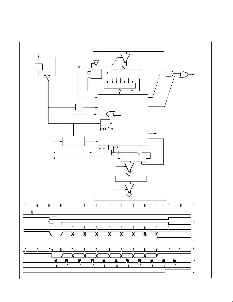
Philips Semiconductors
Product data
P80C3xX2; P80C5xX2;
P87C5xX2
80C51 8-bit microcontroller family
4K/8K/16K/32K ROM/OTP, low voltage (2.7 to 5.5 V),
low power, high speed (30/33 MHz)
2003 Jan 24
27
80C51 Internal Bus
SBUF
Zero Detector
D Q
S
CL
Write
to
SBUF
TX Control
TX Clock
Send
Data
Start
RX Control
Start
RX Clock RI
T1
Serial
Port
Interrupt
Input Shift Register
(9 Bits)
Load
SBUF
Shift
SBUF
Read
SBUF
80C51 Internal Bus
TxD
TB8
˜
16
1-to-0
Transition
Detector
Sample
˜
2
Timer 1
Overflow
SMOD = 1
SMOD = 0
Shift
Bit Detector
Transmit
Send
S1P1
Shift
TX
Clock
Write to SBUF
Start Bit
TxD
Stop Bit
D0
D1
D2
D3
D4
D5
D6
D7
TI
RxD
RX
Clock
˜
16 Reset
Start
Bit
RxD
Stop Bit
D0
D1
D2
D3
D4
D5
D6
D7
Bit Detector
Sample Times
Shift
RI
Receive
Data
˜
16
Load
SBUF
Shift
1FFH
SU00540
Figure 15. Serial Port Mode 1
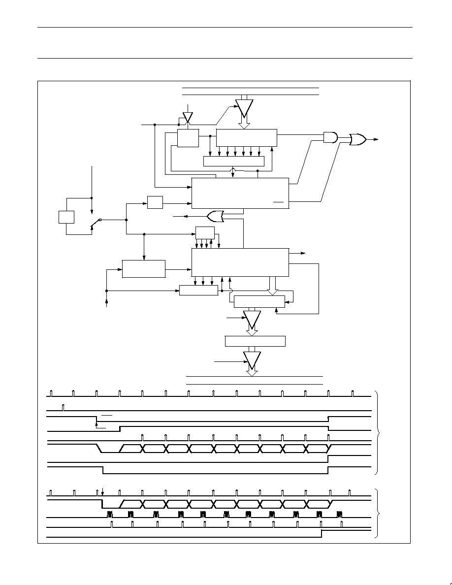
Philips Semiconductors
Product data
P80C3xX2; P80C5xX2;
P87C5xX2
80C51 8-bit microcontroller family
4K/8K/16K/32K ROM/OTP, low voltage (2.7 to 5.5 V),
low power, high speed (30/33 MHz)
2003 Jan 24
28
80C51 Internal Bus
SBUF
Zero Detector
D Q
S
CL
Write
to
SBUF
TX Control
TX Clock
Send
Data
Start
RX Control
Start
Load
SBUF
RX Clock
T1
Serial
Port
Interrupt
Input Shift Register
(9 Bits)
Load
SBUF
Shift
SBUF
Read
SBUF
80C51 Internal Bus
TxD
TB8
˜
16
1-to-0
Transition
Detector
Sample
˜
2
SMOD = 1
SMOD = 0
Shift
Bit Detector
RxD
Stop Bit
Gen.
Mode 2
Phase 2 Clock
(1/2 f
OSC
in
12-clock mode;
f
OSC
in 6-clock
mode)
R1
˜
16
Shift
1FFH
Transmit
Send
S1P1
Shift
TX
Clock
Write to SBUF
Start Bit
TxD
Stop Bit
D0
D1
D2
D3
D4
D5
D6
D7
TI
RX
Clock
˜
16 Reset
Start
Bit
RxD
Stop Bit
D0
D1
D2
D3
D4
D5
D6
D7
Bit Detector
Sample Times
Shift
RI
Receive
Data
(SMOD is
PCON.7)
TB8
RB8
Stop Bit Gen.
SU01627
Figure 16. Serial Port Mode 2
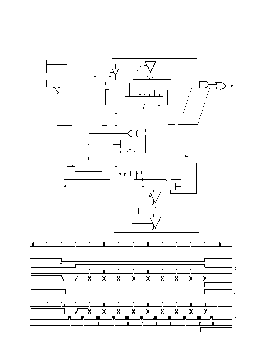
Philips Semiconductors
Product data
P80C3xX2; P80C5xX2;
P87C5xX2
80C51 8-bit microcontroller family
4K/8K/16K/32K ROM/OTP, low voltage (2.7 to 5.5 V),
low power, high speed (30/33 MHz)
2003 Jan 24
29
80C51 Internal Bus
SBUF
Zero Detector
D Q
S
CL
Write
to
SBUF
TX Control
TX Clock
Send
Data
Start
RX Control
Start
RX Clock
T1
Serial
Port
Interrupt
Input Shift Register
(9 Bits)
Load
SBUF
Shift
SBUF
Read
SBUF
80C51 Internal Bus
TxD
TB8
˜
16
1-to-0
Transition
Detector
Sample
˜
2
Timer 1
Overflow
SMOD = 1
SMOD = 0
Shift
Bit Detector
RxD
R1
˜
16
Load
SBUF
Shift
1FFH
Transmit
Send
S1P1
Shift
TX
Clock
Write to SBUF
Start Bit
TxD
Stop Bit
D0
D1
D2
D3
D4
D5
D6
D7
TI
RX
Clock
˜
16 Reset
Start
Bit
RxD
Stop Bit
D0
D1
D2
D3
D4
D5
D6
D7
Bit Detector
Sample Times
Shift
RI
Receive
Data
TB8
RB8
Stop Bit Gen.
SU00542
Figure 17. Serial Port Mode 3

Philips Semiconductors
Product data
P80C3xX2; P80C5xX2;
P87C5xX2
80C51 8-bit microcontroller family
4K/8K/16K/32K ROM/OTP, low voltage (2.7 to 5.5 V),
low power, high speed (30/33 MHz)
2003 Jan 24
30
Enhanced UART operation
In addition to the standard operation modes, the UART can perform
framing error detect by looking for missing stop bits, and automatic
address recognition. The UART also fully supports multiprocessor
communication.
When used for framing error detect the UART looks for missing stop
bits in the communication. A missing bit will set the FE bit in the
SCON register. The FE bit shares the SCON.7 bit with SM0 and the
function of SCON.7 is determined by PCON.6 (SMOD0) (see
Figure 18). If SMOD0 is set then SCON.7 functions as FE. SCON.7
functions as SM0 when SMOD0 is cleared. When used as FE
SCON.7 can only be cleared by software. Refer to Figure 19.
Automatic Address Recognition
Automatic Address Recognition is a feature which allows the UART
to recognize certain addresses in the serial bit stream by using
hardware to make the comparisons. This feature saves a great deal
of software overhead by eliminating the need for the software to
examine every serial address which passes by the serial port. This
feature is enabled by setting the SM2 bit in SCON. In the 9 bit UART
modes, mode 2 and mode 3, the Receive Interrupt flag (RI) will be
automatically set when the received byte contains either the "Given"
address or the "Broadcast" address. The 9 bit mode requires that
the 9th information bit is a 1 to indicate that the received information
is an address and not data. Automatic address recognition is shown
in Figure 20.
The 8 bit mode is called Mode 1. In this mode the RI flag will be set
if SM2 is enabled and the information received has a valid stop bit
following the 8 address bits and the information is either a Given or
Broadcast address.
Mode 0 is the Shift Register mode and SM2 is ignored.
Using the Automatic Address Recognition feature allows a master to
selectively communicate with one or more slaves by invoking the
Given slave address or addresses. All of the slaves may be
contacted by using the Broadcast address. Two special Function
Registers are used to define the slave's address, SADDR, and the
address mask, SADEN. SADEN is used to define which bits in the
SADDR are to be used and which bits are "don't care". The SADEN
mask can be logically ANDed with the SADDR to create the "Given"
address which the master will use for addressing each of the slaves.
Use of the Given address allows multiple slaves to be recognized
while excluding others. The following examples will help to show the
versatility of this scheme:
Slave 0
SADDR
=
1100 0000
SADEN
=
1111 1101
Given
=
1100 00X0
Slave 1
SADDR
=
1100 0000
SADEN
=
1111 1110
Given
=
1100 000X
In the above example SADDR is the same and the SADEN data is
used to differentiate between the two slaves. Slave 0 requires a 0 in
bit 0 and it ignores bit 1. Slave 1 requires a 0 in bit 1 and bit 0 is
ignored. A unique address for Slave 0 would be 1100 0010 since
slave 1 requires a 0 in bit 1. A unique address for slave 1 would be
1100 0001 since a 1 in bit 0 will exclude slave 0. Both slaves can be
selected at the same time by an address which has bit 0 = 0 (for
slave 0) and bit 1 = 0 (for slave 1). Thus, both could be addressed
with 1100 0000.
In a more complex system the following could be used to select
slaves 1 and 2 while excluding slave 0:
Slave 0
SADDR
=
1100 0000
SADEN
=
1111 1001
Given
=
1100 0XX0
Slave 1
SADDR
=
1110 0000
SADEN
=
1111 1010
Given
=
1110 0X0X
Slave 2
SADDR
=
1110 0000
SADEN
=
1111 1100
Given
=
1110 00XX
In the above example the differentiation among the 3 slaves is in the
lower 3 address bits. Slave 0 requires that bit 0 = 0 and it can be
uniquely addressed by 1110 0110. Slave 1 requires that bit 1 = 0 and
it can be uniquely addressed by 1110 and 0101. Slave 2 requires
that bit 2 = 0 and its unique address is 1110 0011. To select Slaves 0
and 1 and exclude Slave 2 use address 1110 0100, since it is
necessary to make bit 2 = 1 to exclude slave 2.
The Broadcast Address for each slave is created by taking the
logical OR of SADDR and SADEN. Zeros in this result are trended
as don't-cares. In most cases, interpreting the don't-cares as ones,
the broadcast address will be FF hexadecimal.
Upon reset SADDR (SFR address 0A9H) and SADEN (SFR
address 0B9H) are leaded with 0s. This produces a given address
of all "don't cares" as well as a Broadcast address of all "don't
cares". This effectively disables the Automatic Addressing mode and
allows the microcontroller to use standard 80C51 type UART drivers
which do not make use of this feature.

Philips Semiconductors
Product data
P80C3xX2; P80C5xX2;
P87C5xX2
80C51 8-bit microcontroller family
4K/8K/16K/32K ROM/OTP, low voltage (2.7 to 5.5 V),
low power, high speed (30/33 MHz)
2003 Jan 24
31
SCON Address = 98H
Reset Value = 0000 0000B
SM0/FE
SM1
SM2
REN
TB8
RB8
Tl
Rl
Bit Addressable
(SMOD0 = 0/1)*
Symbol
Position
Function
FE
SCON.7
Framing Error bit. This bit is set by the receiver when an invalid stop bit is detected. The FE bit is not
cleared by valid frames but should be cleared by software. The SMOD0 bit must be set to enable
access to the FE bit.*
SM0
SCON.7
Serial Port Mode Bit 0, (SMOD0 must = 0 to access bit SM0)
SM1
SCON.6
Serial Port Mode Bit 1
SM2
SCON.5
Enables the Automatic Address Recognition feature in Modes 2 or 3. If SM2 = 1 then Rl will not be set
unless the received 9th data bit (RB8) is 1, indicating an address, and the received byte is a Given or
Broadcast Address. In Mode 1, if SM2 = 1 then Rl will not be activated unless a valid stop bit was
received, and the received byte is a Given or Broadcast Address. In Mode 0, SM2 should be 0.
REN
SCON.4
Enables serial reception. Set by software to enable reception. Clear by software to disable reception.
TB8
SCON.3
The 9th data bit that will be transmitted in Modes 2 and 3. Set or clear by software as desired.
RB8
SCON.2
In modes 2 and 3, the 9th data bit that was received. In Mode 1, if SM2 = 0, RB8 is the stop bit that
was received.
In Mode 0, RB8 is not used.
Tl
SCON.1
Transmit interrupt flag. Set by hardware at the end of the 8th bit time in Mode 0, or at the beginning of
the stop bit in the other modes, in any serial transmission. Must be cleared by software.
Rl
SCON.0
Receive interrupt flag. Set by hardware at the end of the 8th bit time in Mode 0, or halfway through the
stop bit time in the other modes, in any serial reception (except see SM2). Must be cleared by
software.
NOTES:
*SMOD0 is located at PCON.6.
**f
OSC
= oscillator frequency
SU01628
7
6
5
4
3
2
1
0
SM0
SM1
Mode
Description
Baud Rate**
0
0
0
shift register
f
OSC
/12 (12-clk mode) or f
OSC
/6 (6-clk mode)
0
1
1
8-bit UART
variable
1
0
2
9-bit UART
f
OSC
/64 or f
OSC
/32 or f
OSC
/16 (6-clock mode) or
f
OSC
/32 (12-clock mode)
1
1
3
9-bit UART
variable
Figure 18. SCON: Serial Port Control Register
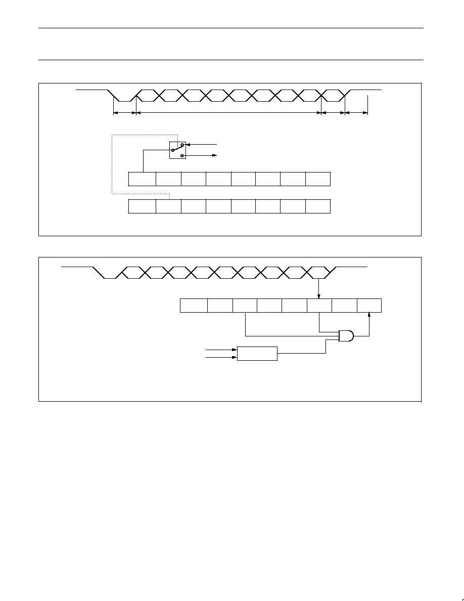
Philips Semiconductors
Product data
P80C3xX2; P80C5xX2;
P87C5xX2
80C51 8-bit microcontroller family
4K/8K/16K/32K ROM/OTP, low voltage (2.7 to 5.5 V),
low power, high speed (30/33 MHz)
2003 Jan 24
32
SMOD1
SMOD0
≠
POF
GF1
GF0
PD
IDL
PCON
(87H)
SM0 / FE
SM1
SM2
REN
TB8
RB8
TI
RI
SCON
(98H)
D0
D1
D2
D3
D4
D5
D6
D7
D8
STOP
BIT
DATA BYTE
ONLY IN
MODE 2, 3
START
BIT
SET FE BIT IF STOP BIT IS 0 (FRAMING ERROR)
SM0 TO UART MODE CONTROL
0 : SCON.7 = SM0
1 : SCON.7 = FE
SU01191
Figure 19. UART Framing Error Detection
SM0
SM1
SM2
REN
TB8
RB8
TI
RI
SCON
(98H)
D0
D1
D2
D3
D4
D5
D6
D7
D8
1
1
1
0
COMPARATOR
1
1
X
RECEIVED ADDRESS D0 TO D7
PROGRAMMED ADDRESS
IN UART MODE 2 OR MODE 3 AND SM2 = 1:
INTERRUPT IF REN=1, RB8=1 AND "RECEIVED ADDRESS" = "PROGRAMMED ADDRESS"
≠ WHEN OWN ADDRESS RECEIVED, CLEAR SM2 TO RECEIVE DATA BYTES
≠ WHEN ALL DATA BYTES HAVE BEEN RECEIVED: SET SM2 TO WAIT FOR NEXT ADDRESS.
SU00045
Figure 20. UART Multiprocessor Communication, Automatic Address Recognition

Philips Semiconductors
Product data
P80C3xX2; P80C5xX2;
P87C5xX2
80C51 8-bit microcontroller family
4K/8K/16K/32K ROM/OTP, low voltage (2.7 to 5.5 V),
low power, high speed (30/33 MHz)
2003 Jan 24
33
Interrupt Priority Structure
IE0
IE1
INT0
IT0
TF0
INT1
IT1
TF1
RI
TI
Interrupt
Sources
0
1
0
1
SU01521
TF2, EXF2
Figure 21. Interrupt Sources
Interrupts
The devices described in this data sheet provide six interrupt
sources. These are shown in Figure 21. The External Interrupts
INT0 and INT1 can each be either level-activated or
transition-activated, depending on bits IT0 and IT1 in Register
TCON. The flags that actually generate these interrupts are bits IE0
and IE1 in TCON. When an external interrupt is generated, the flag
that generated it is cleared by the hardware when the service routine
is vectored to only if the interrupt was transition-activated. If the
interrupt was level-activated, then the external requesting source is
what controls the request flag, rather than the on-chip hardware.
The Timer 0 and Timer 1 Interrupts are generated by TF0 and TF1,
which are set by a rollover in their respective Timer/Counter
registers (except see Timer 0 in Mode 3). When a timer interrupt is
generated, the flag that generated it is cleared by the on-chip
hardware when the service routine is vectored to.
The Serial Port Interrupt is generated by the logical OR of RI and TI.
Neither of these flags is cleared by hardware when the service
routine is vectored to. In fact, the service routine will normally have
to determine whether it was RI or TI that generated the interrupt,
and the bit will have to be cleared in software.
All of the bits that generate interrupts can be set or cleared by
software, with the same result as though it had been set or cleared
by hardware. That is, interrupts can be generated or pending
interrupts can be canceled in software.
Each of these interrupt sources can be individually enabled or
disabled by setting or clearing a bit in Special Function Register IE
(Figure 22). IE also contains a global disable bit, EA, which disables
all interrupts at once.
Priority Level Structure
Each interrupt source can also be individually programmed to one of
four priority levels by setting or clearing bits in Special Function
Registers IP (Figure 23) and IPH (Figure 24). A lower-priority
interrupt can itself be interrupted by a higher-priority interrupt, but
not by another interrupt of the same level. A high-priority level 3
interrupt can't be interrupted by any other interrupt source.
If two request of different priority levels are received simultaneously,
the request of higher priority level is serviced. If requests of the
same priority level are received simultaneously, an internal polling
sequence determines which request is serviced. Thus within each
priority level there is a second priority structure determined by the
polling sequence as follows:
Source
Priority Within Level
1. IE0 (External Int 0)
(highest)
2. TF0 (Timer 0)
3. IE1 (External Int 1)
4. TF1 (Timer 1)
5. RI+TI (UART)
6. TF2, EXF2 (Timer 2)
(lowest)
Note that the "priority within level" structure is only used to resolve
simultaneous requests of the same priority level.
The IP and IPH registers contain a number of unimplemented bits.
User software should not write 1s to these positions, since they may
be used in other 80C51 Family products.
How Interrupts Are Handled
The interrupt flags are sampled at S5P2 of every machine cycle.
The samples are polled during the following machine cycle. If one of
the flags was in a set condition at S5P2 of the preceding cycle, the
polling cycle will find it and the interrupt system will generate an
LCALL to the appropriate service routine, provided this
hardware-generated LCALL is not blocked by any of the following
conditions:
1. An interrupt of equal or higher priority level is already in
progress.
2. The current (polling) cycle is not the final cycle in the execution
of the instruction in progress.
3. The instruction in progress is RETI or any write to the IE or IP
registers.
Any of these three conditions will block the generation of the LCALL
to the interrupt service routine. Condition 2 ensures that the
instruction in progress will be completed before vectoring to any
service routine. Condition 3 ensures that if the instruction in
progress is RETI or any access to IE or IP, then at least one more
instruction will be executed before any interrupt is vectored to.
The polling cycle is repeated with each machine cycle, and the
values polled are the values that were present at S5P2 of the
previous machine cycle. Note that if an interrupt flag is active but not
being responded to for one of the above conditions, if the flag is not
still active when the blocking condition is removed, the denied
interrupt will not be serviced. In other words, the fact that the
interrupt flag was once active but not serviced is not remembered.
Every polling cycle is new.

Philips Semiconductors
Product data
P80C3xX2; P80C5xX2;
P87C5xX2
80C51 8-bit microcontroller family
4K/8K/16K/32K ROM/OTP, low voltage (2.7 to 5.5 V),
low power, high speed (30/33 MHz)
2003 Jan 24
34
EX0
Enable Bit = 1 enables the interrupt.
Enable Bit = 0 disables it.
BIT
SYMBOL
FUNCTION
IE.7
EA
Global disable bit. If EA = 0, all interrupts are disabled. If EA = 1, each interrupt can be individually
enabled or disabled by setting or clearing its enable bit.
IE.6
--
Not implemented. Reserved for future use.
IE.5
ET2
Timer 2 interrupt enable bit.
IE.4
ES
Serial Port interrupt enable bit.
IE.3
ET1
Timer 1 interrupt enable bit.
IE.2
EX1
External interrupt 1 enable bit.
IE.1
ET0
Timer 0 interrupt enable bit.
IE.0
EX0
External interrupt 0 enable bit.
SU01522
ET0
EX1
ET1
ES
ET2
--
EA
0
1
2
3
4
5
6
7
IE
Address = 0A8H
Bit Addressable
Reset Value = 0X000000B
Figure 22. Interrupt Enable (IE) Register
PX0
Priority Bit = 1 assigns higher priority
Priority Bit = 0 assigns lower priority
BIT
SYMBOL
FUNCTION
IP.7
--
Not implemented, reserved for future use.
IP.6
--
Not implemented, reserved for future use.
IP.5
PT2
Timer 2 interrupt priority bit.
IP.4
PS
Serial Port interrupt priority bit.
IP.3
PT1
Timer 1 interrupt priority bit.
IP.2
PX1
External interrupt 1 priority bit.
IP.1
PT0
Timer 0 interrupt priority bit.
IP.0
PX0
External interrupt 0 priority bit.
SU01523
PT0
PX1
PT1
PS
PT2
--
--
0
1
2
3
4
5
6
7
IP
Address = 0B8H
Bit Addressable
Reset Value = xx000000B
Figure 23. Interrupt Priority (IP) Register
PX0H
Priority Bit = 1 assigns higher priority
Priority Bit = 0 assigns lower priority
BIT
SYMBOL
FUNCTION
IPH.7
--
Not implemented, reserved for future use.
IPH.6
--
Not implemented, reserved for future use.
IPH.5
PT2H
Timer 2 interrupt priority bit high.
IPH.4
PSH
Serial Port interrupt priority bit high.
IPH.3
PT1H
Timer 1 interrupt priority bit high.
IPH.2
PX1H
External interrupt 1 priority bit high.
IPH.1
PT0H
Timer 0 interrupt priority bit high.
IPH.0
PX0H
External interrupt 0 priority bit high.
SU01524
PT0H
PX1H
PT1H
PSH
PT2H
--
--
0
1
2
3
4
5
6
7
IPH
Address = B7H
Bit Addressable
Reset Value = xx000000B
Figure 24. Interrupt Priority HIGH (IPH) Register
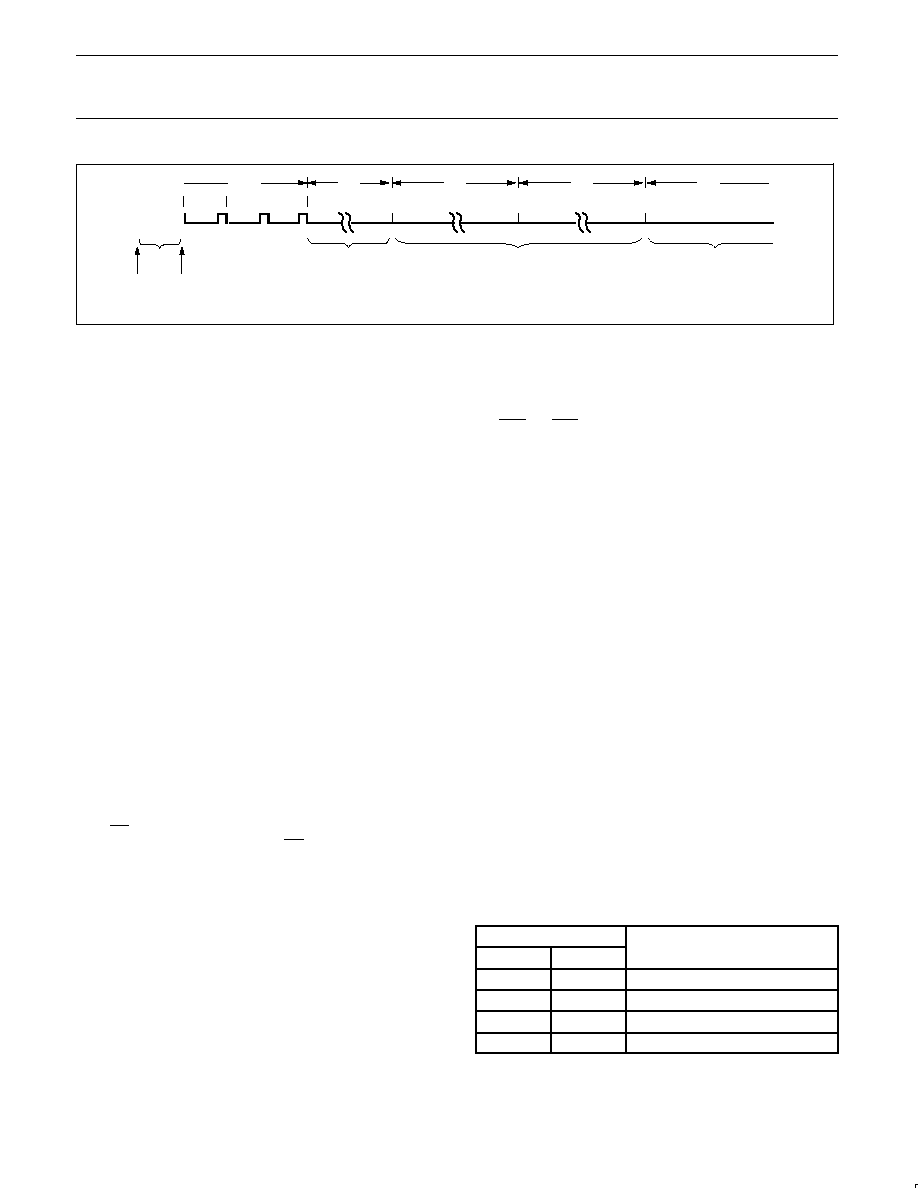
Philips Semiconductors
Product data
P80C3xX2; P80C5xX2;
P87C5xX2
80C51 8-bit microcontroller family
4K/8K/16K/32K ROM/OTP, low voltage (2.7 to 5.5 V),
low power, high speed (30/33 MHz)
2003 Jan 24
35
. . . .
C1
C2
C3
C4
C5
. . . .
. . . .
Interrupts
Are Polled
Long Call to
Interrupt
Vector Address
Interrupt Routine
Interrupt
Goes
Active
. . . . . . . . .
Interrupt
Latched
This is the fastest possible response when C2 is the final cycle of an instruction other than RETI or an access to IE or IP.
S5P2
S6
. . . . . . . . .
SU00546
Figure 25. Interrupt Response Timing Diagram
The polling cycle/LCALL sequence is illustrated in Figure 25.
Note that if an interrupt of higher priority level goes active prior to
S5P2 of the machine cycle labeled C3 in Figure 25, then in
accordance with the above rules it will be vectored to during C5 and
C6, without any instruction of the lower priority routine having been
executed.
Thus the processor acknowledges an interrupt request by executing
a hardware-generated LCALL to the appropriate servicing routine. In
some cases it also clears the flag that generated the interrupt, and in
other cases it doesn't. It never clears the Serial Port flag. This has to
be done in the user's software. It clears an external interrupt flag
(IE0 or IE1) only if it was transition-activated. The
hardware-generated LCALL pushes the contents of the Program
Counter on to the stack (but it does not save the PSW) and reloads
the PC with an address that depends on the source of the interrupt
being vectored to, as shown in Table 8.
Execution proceeds from that location until the RETI instruction is
encountered. The RETI instruction informs the processor that this
interrupt routine is no longer in progress, then pops the top two
bytes from the stack and reloads the Program Counter. Execution of
the interrupted program continues from where it left off.
Note that a simple RET instruction would also have returned
execution to the interrupted program, but it would have left the
interrupt control system thinking an interrupt was still in progress,
making future interrupts impossible.
External Interrupts
The external sources can be programmed to be level-activated or
transition-activated by setting or clearing bit IT1 or IT0 in Register
TCON. If ITx = 0, external interrupt x is triggered by a detected low
at the INTx pin. If ITx = 1, external interrupt x is edge triggered. In
this mode if successive samples of the INTx pin show a high in one
cycle and a low in the next cycle, interrupt request flag IEx in TCON
is set. Flag bit IEx then requests the interrupt.
Since the external interrupt pins are sampled once each machine
cycle, an input high or low should hold for at least 12 oscillator
periods to ensure sampling. If the external interrupt is
transition-activated, the external source has to hold the request pin
high for at least one cycle, and then hold it low for at least one cycle.
This is done to ensure that the transition is seen so that interrupt
request flag IEx will be set. IEx will be automatically cleared by the
CPU when the service routine is called.
If the external interrupt is level-activated, the external source has to
hold the request active until the requested interrupt is actually
generated. Then it has to deactivate the request before the interrupt
service routine is completed, or else another interrupt will be
generated.
Response Time
The INT0 and INT1 levels are inverted and latched into IE0 and IE1
at S5P2 of every machine cycle. The values are not actually polled
by the circuitry until the next machine cycle. If a request is active
and conditions are right for it to be acknowledged, a hardware
subroutine call to the requested service routine will be the next
instruction to be executed. The call itself takes two cycles. Thus, a
minimum of three complete machine cycles elapse between
activation of an external interrupt request and the beginning of
execution of the first instruction of the service routine. Figure 25
shows interrupt response timings.
A longer response time would result if the request is blocked by one
of the 3 previously listed conditions. If an interrupt of equal or higher
priority level is already in progress, the additional wait time obviously
depends on the nature of the other interrupt's service routine. If the
instruction in progress is not in its final cycle, the additional wait time
cannot be more the 3 cycles, since the longest instructions (MUL
and DIV) are only 4 cycles long, and if the instruction in progress is
RETI or an access to IE or IP, the additional wait time cannot be
more than 5 cycles (a maximum of one more cycle to complete the
instruction in progress, plus 4 cycles to complete the next instruction
if the instruction is MUL or DIV).
Thus, in a single-interrupt system, the response time is always more
than 3 cycles and less than 9 cycles.
As previously mentioned, the derivatives described in this data
sheet have a four-level interrupt structure. The corresponding
registers are IE, IP and IPH. (See Figures 22, 23, and 24.) The IPH
(Interrupt Priority High) register makes the four-level interrupt
structure possible.
The function of the IPH SFR is simple and when combined with the
IP SFR determines the priority of each interrupt. The priority of each
interrupt is determined as shown in the following table:
PRIORITY BITS
INTERRUPT PRIORITY LEVEL
IPH.x
IP.x
INTERRUPT PRIORITY LEVEL
0
0
Level 0 (lowest priority)
0
1
Level 1
1
0
Level 2
1
1
Level 3 (highest priority)
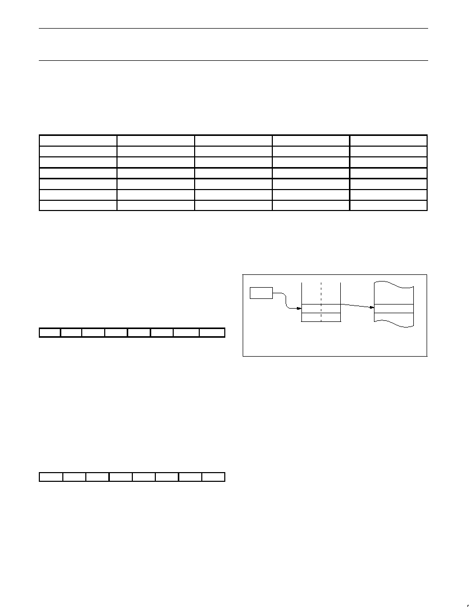
Philips Semiconductors
Product data
P80C3xX2; P80C5xX2;
P87C5xX2
80C51 8-bit microcontroller family
4K/8K/16K/32K ROM/OTP, low voltage (2.7 to 5.5 V),
low power, high speed (30/33 MHz)
2003 Jan 24
36
An interrupt will be serviced as long as an interrupt of equal or
higher priority is not already being serviced. If an interrupt of equal
or higher level priority is being serviced, the new interrupt will wait
until it is finished before being serviced. If a lower priority level
interrupt is being serviced, it will be stopped and the new interrupt
serviced. When the new interrupt is finished, the lower priority level
interrupt that was stopped will be completed.
Table 8.
Interrupt Table
SOURCE
POLLING PRIORITY
REQUEST BITS
HARDWARE CLEAR?
VECTOR ADDRESS
External interrupt 0
1
IE0
N (L)
1
Y (T)
2
03H
Timer 0
2
TF0
Y
0BH
External interrupt 1
3
IE1
N (L)
Y (T)
13H
Timer 1
4
TF1
Y
1BH
UART
5
RI, TI
N
23H
Timer 2
6
TF2, EXF2
N
2BH
NOTES:
1. L = Level activated
2. T = Transition activated
Reduced EMI
All port pins have slew rate controlled outputs. This is to limit noise
generated by quickly switching output signals. The slew rate is
factory set to approximately 10 ns rise and fall times.
Reduced EMI Mode
The AO bit (AUXR.0) in the AUXR register when set disables the
ALE output.
AUXR (8EH)
7
6
5
4
3
2
1
0
≠
≠
≠
≠
≠
≠
≠
AO
AUXR.0
AO
Turns off ALE output.
Dual DPTR
The dual DPTR structure (see Figure 26) enables a way to specify
the address of an external data memory location. There are two
16-bit DPTR registers that address the external memory, and a
single bit called DPS = AUXR1/bit0 that allows the program code to
switch between them.
∑
New Register Name: AUXR1#
∑
SFR Address: A2H
∑
Reset Value: xxx000x0B
AUXR1 (A2H)
7
6
5
4
3
2
1
0
≠
≠
≠
LPEP
WUPD
0
≠
DPS
Where:
DPS = AUXR1/bit0 = Switches between DPTR0 and DPTR1.
Select Reg
DPS
DPTR0
0
DPTR1
1
The DPS bit status should be saved by software when switching
between DPTR0 and DPTR1.
Note that bit 2 is not writable and is always read as a zero. This
allows the DPS bit to be quickly toggled simply by executing an INC
DPTR instruction without affecting the WUPD or LPEP bits.
DPS
DPTR1
DPTR0
DPH
(83H)
DPL
(82H)
EXTERNAL
DATA
MEMORY
SU00745A
BIT0
AUXR1
Figure 26.
DPTR Instructions
The instructions that refer to DPTR refer to the data pointer that is
currently selected using the AUXR1/bit 0 register. The six
instructions that use the DPTR are as follows:
INC DPTR
Increments the data pointer by 1
MOV DPTR, #data16
Loads the DPTR with a 16-bit constant
MOV A, @ A+DPTR
Move code byte relative to DPTR to ACC
MOVX A, @ DPTR
Move external RAM (16-bit address) to
ACC
MOVX @ DPTR , A
Move ACC to external RAM (16-bit
address)
JMP @ A + DPTR
Jump indirect relative to DPTR
The data pointer can be accessed on a byte-by-byte basis by
specifying the low or high byte in an instruction which accesses the
SFRs. See application note AN458 for more details.

Philips Semiconductors
Product data
P80C3xX2; P80C5xX2;
P87C5xX2
80C51 8-bit microcontroller family
4K/8K/16K/32K ROM/OTP, low voltage (2.7 to 5.5 V),
low power, high speed (30/33 MHz)
2003 Jan 24
37
ABSOLUTE MAXIMUM RATINGS
1, 2, 3
PARAMETER
RATING
UNIT
Operating temperature under bias
0 to +70 or ≠40 to +85
∞
C
Storage temperature range
≠65 to +150
∞
C
Voltage on EA/V
PP
pin to V
SS
0 to +13.0
V
Voltage on any other pin to V
SS
≠0.5 to +6.5
V
Maximum I
OL
per I/O pin
15
mA
Power dissipation (based on package heat transfer limitations, not device power consumption)
1.5
W
NOTES:
1. Stresses above those listed under Absolute Maximum Ratings may cause permanent damage to the device. This is a stress rating only and
functional operation of the device at these or any conditions other than those described in the AC and DC Electrical Characteristics section
of this specification is not implied.
2. This product includes circuitry specifically designed for the protection of its internal devices from the damaging effects of excessive static
charge. Nonetheless, it is suggested that conventional precautions be taken to avoid applying greater than the rated maximum.
3. Parameters are valid over operating temperature range unless otherwise specified. All voltages are with respect to V
SS
unless otherwise
noted.
AC ELECTRICAL CHARACTERISTICS
T
amb
= 0
∞
C to +70
∞
C or ≠40
∞
C to +85
∞
C
CLOCK FREQUENCY
RANGE
SYMBOL
FIGURE
PARAMETER
OPERATING MODE
POWER SUPPLY
VOLTAGE
MIN
MAX
UNIT
1/t
CLCL
31
Oscillator frequency
6-clock
5 V
"
10%
0
30
MHz
6-clock
2.7 V to 5.5 V
0
16
MHz
12-clock
5 V
"
10%
0
33
MHz
12-clock
2.7 V to 5.5 V
0
16
MHz
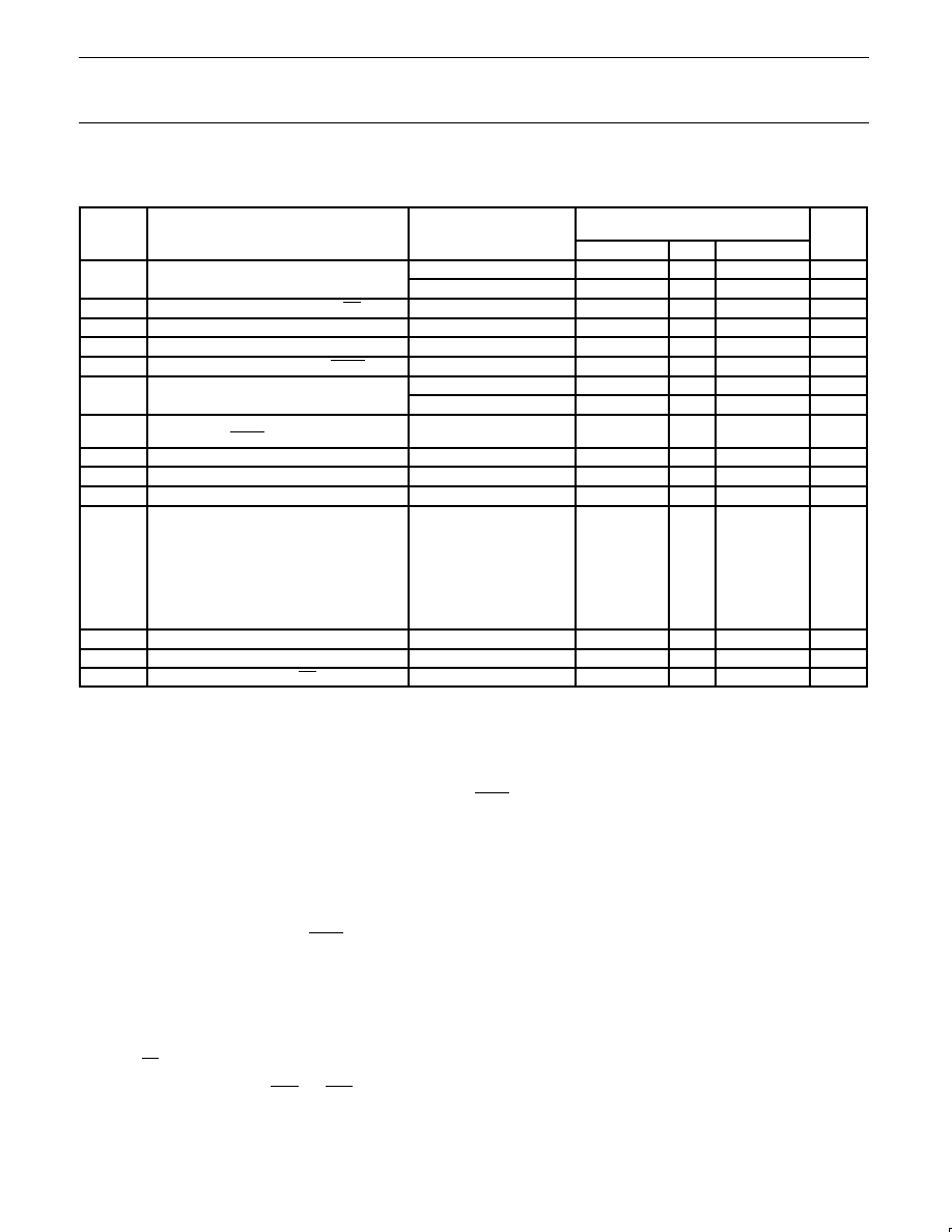
Philips Semiconductors
Product data
P80C3xX2; P80C5xX2;
P87C5xX2
80C51 8-bit microcontroller family
4K/8K/16K/32K ROM/OTP, low voltage (2.7 to 5.5 V),
low power, high speed (30/33 MHz)
2003 Jan 24
38
DC ELECTRICAL CHARACTERISTICS
T
amb
= 0
∞
C to +70
∞
C or ≠40
∞
C to +85
∞
C; V
CC
= 2.7 V to 5.5 V; V
SS
= 0 V (16 MHz max. CPU clock)
SYMBOL
PARAMETER
TEST
CONDITIONS
LIMITS
UNIT
MIN
TYP
1
MAX
V
IL
Input low voltage
11
4.0 V < V
CC
< 5.5 V
≠0.5
0.2 V
CC
≠0.1
V
2.7 V < V
CC
< 4.0 V
≠0.5
0.7 V
CC
V
V
IH
Input high voltage (ports 0, 1, 2, 3, EA)
≠
0.2 V
CC
+0.9
V
CC
+0.5
V
V
IH1
Input high voltage, XTAL1, RST
11
≠
0.7 V
CC
V
CC
+0.5
V
V
OL
Output low voltage, ports 1, 2,
8
V
CC
= 2.7 V; I
OL
= 1.6 mA
2
≠
0.4
V
V
OL1
Output low voltage, port 0, ALE, PSEN
8, 7
V
CC
= 2.7 V; I
OL
= 3.2 mA
2
≠
0.4
V
V
OH
Output high voltage, ports 1, 2, 3
3
V
CC
= 2.7 V; I
OH
= ≠20
m
A
V
CC
≠ 0.7
≠
V
V
CC
= 4.5 V; I
OH
= ≠30
m
A
V
CC
≠ 0.7
≠
V
V
OH1
Output high voltage (port 0 in external bus
mode), ALE
9
, PSEN
3
V
CC
= 2.7 V; I
OH
= ≠3.2 mA
V
CC
≠ 0.7
≠
V
I
IL
Logical 0 input current, ports 1, 2, 3
V
IN
= 0.4 V
≠1
≠50
m
A
I
TL
Logical 1-to-0 transition current, ports 1, 2, 3
6
V
IN
= 2.0 V; See note 4
≠
≠650
m
A
I
LI
Input leakage current, port 0
0.45 < V
IN
< V
CC
≠ 0.3
≠
±
10
m
A
I
CC
Power supply current (see Figure 34 and
Source Code):
Active mode @ 16 MHz
m
A
Idle mode @ 16 MHz
m
A
Power-down mode or clock stopped
(see Figure 30 for conditions)
12
T
amb
= 0
∞
C to 70
∞
C
2
30
m
A
T
amb
= ≠40
∞
C to +85
∞
C
3
50
m
A
V
RAM
RAM keep-alive voltage
≠
1.2
V
R
RST
Internal reset pull-down resistor
≠
40
225
k
C
IO
Pin capacitance
10
(except EA)
≠
≠
15
pF
NOTES:
1. Typical ratings are not guaranteed. Values listed are based on tests conducted on limited number of samples at room temperature.
2. Capacitive loading on ports 0 and 2 may cause spurious noise to be superimposed on the V
OL
s of ALE and ports 1 and 3. The noise is
due to external bus capacitance discharging into the port 0 and port 2 pins when these pins make 1-to-0 transitions during bus operations.
In the worst cases (capacitive loading > 100 pF), the noise pulse on the ALE pin may exceed 0.8 V. In such cases, it may be desirable to
qualify ALE with a Schmitt Trigger, or use an address latch with a Schmitt Trigger STROBE input. I
OL
can exceed these conditions provided
that no single output sinks more than 5 mA and no more than two outputs exceed the test conditions.
3. Capacitive loading on ports 0 and 2 may cause the V
OH
on ALE and PSEN to momentarily fall below the V
CC
≠0.7 specification when the
address bits are stabilizing.
4. Pins of ports 1, 2 and 3 source a transition current when they are being externally driven from 1 to 0. The transition current reaches its
maximum value when V
IN
is approximately 2 V.
5. See Figures 36 through 39 for I
CC
test conditions and Figure 34 for I
CC
vs. Frequency
12-clock mode characteristics:
Active mode (operating):
I
CC
= 1.0 mA + 0.9 mA
◊
FREQ.[MHz]
Active mode (reset):
I
CC
= 7.0 mA + 0.5 mA x FREQ.[MHz]
Idle mode:
I
CC
= 1.0 mA + 0.18 mA x FREQ.[MHz]
6. This value applies to T
amb
= 0
∞
C to +70
∞
C. For T
amb
= ≠40
∞
C to +85
∞
C, I
TL
= ≠750
m
A.
7. Load capacitance for port 0, ALE, and PSEN = 100 pF, load capacitance for all other outputs = 80 pF.
8. Under steady state (non-transient) conditions, I
OL
must be externally limited as follows:
Maximum I
OL
per port pin:
15 mA (*NOTE: This is 85
∞
C specification.)
Maximum I
OL
per 8-bit port:
26 mA
Maximum total I
OL
for all outputs:
71 mA
If I
OL
exceeds the test condition, V
OL
may exceed the related specification. Pins are not guaranteed to sink current greater than the listed
test conditions.
9. ALE is tested to V
OH1
, except when ALE is off then V
OH
is the voltage specification.
10. Pin capacitance is characterized but not tested. Pin capacitance is less than 25 pF. Pin capacitance of ceramic package is less than 15 pF
(except EA is 25 pF).
11. To improve noise rejection a nominal 100 ns glitch rejection circuitry has been added to the RST pin, and a nominal 15 ns glitch rejection
circuitry has been added to the INT0 and INT1 pins. Previous devices provided only an inherent 5 ns of glitch rejection.
12. Power down mode for 3 V range: Commercial Temperature Range ≠ typ: 0.5
m
A, max. 20
m
A; Industrial Temperature Range ≠ typ. 1.0
m
A,
max. 30
m
A;
Philips Semiconductors
Product data
P80C3xX2; P80C5xX2;
P87C5xX2
80C51 8-bit microcontroller family
4K/8K/16K/32K ROM/OTP, low voltage (2.7 to 5.5 V),
low power, high speed (30/33 MHz)
2003 Jan 24
39
DC ELECTRICAL CHARACTERISTICS
T
amb
= 0
∞
C to +70
∞
C or ≠40
∞
C to +85
∞
C; V
CC
= 5 V
±
10%; V
SS
= 0 V (30/33 MHz max. CPU clock)
SYMBOL
PARAMETER
TEST
CONDITIONS
LIMITS
UNIT
MIN
TYP
1
MAX
V
IL
Input low voltage
11
4.5 V < V
CC
< 5.5 V
≠0.5
0.2 V
CC
≠0.1
V
V
IH
Input high voltage (ports 0, 1, 2, 3, EA)
≠
0.2 V
CC
+0.9
V
CC
+0.5
V
V
IH1
Input high voltage, XTAL1, RST
11
≠
0.7 V
CC
V
CC
+0.5
V
V
OL
Output low voltage, ports 1, 2, 3
8
V
CC
= 4.5 V; I
OL
= 1.6 mA
2
≠
0.4
V
V
OL1
Output low voltage, port 0, ALE, PSEN
7, 8
V
CC
= 4.5 V; I
OL
= 3.2 mA
2
≠
0.4
V
V
OH
Output high voltage, ports 1, 2, 3
3
V
CC
= 4.5 V; I
OH
= ≠30
m
A
V
CC
≠ 0.7
≠
V
V
OH1
Output high voltage (port 0 in external bus
mode), ALE
9
, PSEN
3
V
CC
= 4.5 V; I
OH
= ≠3.2 mA
V
CC
≠ 0.7
≠
V
I
IL
Logical 0 input current, ports 1, 2, 3
V
IN
= 0.4 V
≠1
≠50
m
A
I
TL
Logical 1-to-0 transition current, ports 1, 2, 3
6
V
IN
= 2.0 V; See note 4
≠
≠650
m
A
I
LI
Input leakage current, port 0
0.45 < V
IN
< V
CC
≠ 0.3
≠
±
10
m
A
I
CC
Power supply current (see Figure 34):
Active mode (see Note 5)
Idle mode (see Note 5)
Power-down mode or clock stopped
(see Figure 39 for conditions)
T
amb
= 0
∞
C to 70
∞
C
2
30
m
A
T
amb
= ≠40
∞
C to +85
∞
C
3
50
m
A
V
RAM
RAM keep-alive voltage
≠
1.2
V
R
RST
Internal reset pull-down resistor
≠
40
225
k
C
IO
Pin capacitance
10
(except EA)
≠
≠
15
pF
NOTES:
1. Typical ratings are not guaranteed. The values listed are at room temperature, 5 V.
2. Capacitive loading on ports 0 and 2 may cause spurious noise to be superimposed on the V
OL
s of ALE and ports 1 and 3. The noise is due
to external bus capacitance discharging into the port 0 and port 2 pins when these pins make 1-to-0 transitions during bus operations. In the
worst cases (capacitive loading > 100 pF), the noise pulse on the ALE pin may exceed 0.8 V. In such cases, it may be desirable to qualify
ALE with a Schmitt Trigger, or use an address latch with a Schmitt Trigger STROBE input. I
OL
can exceed these conditions provided that no
single output sinks more than 5 mA and no more than two outputs exceed the test conditions.
3. Capacitive loading on ports 0 and 2 may cause the V
OH
on ALE and PSEN to momentarily fall below the V
CC
≠0.7 specification when the
address bits are stabilizing.
4. Pins of ports 1, 2 and 3 source a transition current when they are being externally driven from 1 to 0. The transition current reaches its
maximum value when V
IN
is approximately 2 V.
5. See Figures 36 through 39 for I
CC
test conditions and Figure 34 for I
CC
vs. Frequency.
12-clock mode characteristics:
Active mode (operating):
I
CC(MAX)
= 1.0 mA + 0.9 mA
◊
FREQ.[MHz]
Active mode (reset):
I
CC(MAX)
= 7.0 mA + 0.5 mA x FREQ.[MHz]
Idle mode:
I
CC(MAX)
= 1.0 mA + 0.18 mA
◊
FREQ.[MHz]
6. This value applies to T
amb
= 0
∞
C to +70
∞
C. For T
amb
= ≠40
∞
C to +85
∞
C, I
TL
= ≠750
µ
.
7. Load capacitance for port 0, ALE, and PSEN = 100 pF, load capacitance for all other outputs = 80 pF.
8. Under steady state (non-transient) conditions, I
OL
must be externally limited as follows:
Maximum I
OL
per port pin:
15 mA (*NOTE: This is 85
∞
C specification.)
Maximum I
OL
per 8-bit port:
26 mA
Maximum total I
OL
for all outputs:
71 mA
If I
OL
exceeds the test condition, V
OL
may exceed the related specification. Pins are not guaranteed to sink current greater than the listed
test conditions.
9. ALE is tested to V
OH1
, except when ALE is off then V
OH
is the voltage specification.
10. Pin capacitance is characterized but not tested. Pin capacitance is less than 25 pF. Pin capacitance of ceramic package is less than 15 pF
(except EA is 25 pF).
11. To improve noise rejection a nominal 100 ns glitch rejection circuitry has been added to the RST pin, and a nominal 15 ns glitch rejection
circuitry has been added to the INT0 and INT1 pins. Previous devices provided only an inherent 5 ns of glitch rejection.
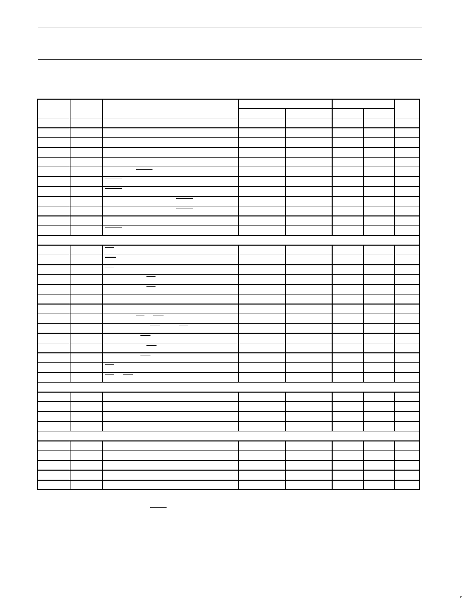
Philips Semiconductors
Product data
P80C3xX2; P80C5xX2;
P87C5xX2
80C51 8-bit microcontroller family
4K/8K/16K/32K ROM/OTP, low voltage (2.7 to 5.5 V),
low power, high speed (30/33 MHz)
2003 Jan 24
40
AC ELECTRICAL CHARACTERISTICS (12-CLOCK MODE, 5 V
±
10% OPERATION)
T
amb
= 0
∞
C to +70
∞
C or ≠40
∞
C to +85
∞
C ; V
CC
= 5 V
±
10%, V
SS
= 0 V
1,2,3,4
Symbol
Figure
Parameter
Limits
16 MHz Clock
Unit
MIN
MAX
MIN
MAX
1/t
CLCL
31
Oscillator frequency
0
33
≠
≠
MHz
t
LHLL
27
ALE pulse width
2 t
CLCL
≠8
≠
117
≠
ns
t
AVLL
27
Address valid to ALE low
t
CLCL
≠13
≠
49.5
≠
ns
t
LLAX
27
Address hold after ALE low
t
CLCL
≠20
≠
42.5
≠
ns
t
LLIV
27
ALE low to valid instruction in
≠
4 t
CLCL
≠35
≠
215
ns
t
LLPL
27
ALE low to PSEN low
t
CLCL
≠10
≠
52.5
≠
ns
t
PLPH
27
PSEN pulse width
3 t
CLCL
≠10
≠
177.5
≠
ns
t
PLIV
27
PSEN low to valid instruction in
≠
3 t
CLCL
≠35
≠
152.5
ns
t
PXIX
27
Input instruction hold after PSEN
0
≠
0
≠
ns
t
PXIZ
27
Input instruction float after PSEN
≠
t
CLCL
≠10
≠
52.5
ns
t
AVIV
27
Address to valid instruction in
≠
5 t
CLCL
≠35
≠
277.5
ns
t
PLAZ
27
PSEN low to address float
≠
10
≠
10
ns
Data Memory
t
RLRH
28
RD pulse width
6 t
CLCL
≠20
≠
355
≠
ns
t
WLWH
29
WR pulse width
6 t
CLCL
≠20
≠
355
≠
ns
t
RLDV
28
RD low to valid data in
≠
5 t
CLCL
≠35
≠
277.5
ns
t
RHDX
28
Data hold after RD
0
≠
0
≠
ns
t
RHDZ
28
Data float after RD
≠
2 t
CLCL
≠10
≠
115
ns
t
LLDV
28
ALE low to valid data in
≠
8 t
CLCL
≠35
≠
465
ns
t
AVDV
28
Address to valid data in
≠
9 t
CLCL
≠35
≠
527.5
ns
t
LLWL
28, 29
ALE low to RD or WR low
3 t
CLCL
≠15
3 t
CLCL
+15
172.5
202.5
ns
t
AVWL
28, 29
Address valid to WR low or RD low
4 t
CLCL
≠15
≠
235
≠
ns
t
QVWX
29
Data valid to WR transition
t
CLCL
≠25
≠
37.5
≠
ns
t
WHQX
29
Data hold after WR
t
CLCL
≠15
≠
47.5
≠
ns
t
QVWH
29
Data valid to WR high
7 t
CLCL
≠5
≠
432.5
≠
ns
t
RLAZ
28
RD low to address float
≠
0
≠
0
ns
t
WHLH
28, 29
RD or WR high to ALE high
t
CLCL
≠10
t
CLCL
+10
52.5
72.5
ns
External Clock
t
CHCX
31
High time
0.32 t
CLCL
t
CLCL
≠ t
CLCX
≠
≠
ns
t
CLCX
31
Low time
0.32 t
CLCL
t
CLCL
≠ t
CHCX
≠
≠
ns
t
CLCH
31
Rise time
≠
5
≠
≠
ns
t
CHCL
31
Fall time
≠
5
≠
≠
ns
Shift register
t
XLXL
30
Serial port clock cycle time
12 t
CLCL
≠
750
≠
ns
t
QVXH
30
Output data setup to clock rising edge
10 t
CLCL
≠25
≠
600
≠
ns
t
XHQX
30
Output data hold after clock rising edge
2 t
CLCL
≠15
≠
110
≠
ns
t
XHDX
30
Input data hold after clock rising edge
0
≠
0
≠
ns
t
XHDV
30
Clock rising edge to input data valid
≠
10 t
CLCL
≠133
≠
492
ns
NOTES:
1. Parameters are valid over operating temperature range unless otherwise specified.
2. Load capacitance for port 0, ALE, and PSEN = 100 pF, load capacitance for all outputs = 80 pF
3. Interfacing the microcontroller to devices with float time up to 45 ns is permitted. This limited bus contention will not cause damage to port 0
drivers.
4. Parts are guaranteed by design to operate down to 0 Hz.

Philips Semiconductors
Product data
P80C3xX2; P80C5xX2;
P87C5xX2
80C51 8-bit microcontroller family
4K/8K/16K/32K ROM/OTP, low voltage (2.7 to 5.5 V),
low power, high speed (30/33 MHz)
2003 Jan 24
41
AC ELECTRICAL CHARACTERISTICS (12-CLOCK MODE, 2.7 V TO 5.5 V OPERATION)
T
amb
= 0
∞
C to +70
∞
C or ≠40
∞
C to +85
∞
C ; V
CC
= 2.7 V to 5.5 V, V
SS
= 0 V
1,2,3,4
Symbol
Figure
Parameter
Limits
16 MHz Clock
Unit
MIN
MAX
MIN
MAX
1/t
CLCL
31
Oscillator frequency
0
16
≠
≠
MHz
t
LHLL
27
ALE pulse width
2t
CLCL
≠10
≠
115
≠
ns
t
AVLL
27
Address valid to ALE low
t
CLCL
≠15
≠
47.5
≠
ns
t
LLAX
27
Address hold after ALE low
t
CLCL
≠25
≠
37.5
≠
ns
t
LLIV
27
ALE low to valid instruction in
≠
4 t
CLCL
≠55
≠
195
ns
t
LLPL
27
ALE low to PSEN low
t
CLCL
≠15
≠
47.5
≠
ns
t
PLPH
27
PSEN pulse width
3 t
CLCL
≠15
≠
172.5
≠
ns
t
PLIV
27
PSEN low to valid instruction in
≠
3 t
CLCL
≠55
≠
132.5
ns
t
PXIX
27
Input instruction hold after PSEN
0
≠
0
≠
ns
t
PXIZ
27
Input instruction float after PSEN
≠
t
CLCL
≠10
≠
52.5
ns
t
AVIV
27
Address to valid instruction in
≠
5 t
CLCL
≠50
≠
262.5
ns
t
PLAZ
27
PSEN low to address float
≠
10
≠
10
ns
Data Memory
t
RLRH
28
RD pulse width
6 t
CLCL
≠25
≠
350
≠
ns
t
WLWH
29
WR pulse width
6 t
CLCL
≠25
≠
350
≠
ns
t
RLDV
28
RD low to valid data in
≠
5 t
CLCL
≠50
≠
262.5
ns
t
RHDX
28
Data hold after RD
0
≠
0
≠
ns
t
RHDZ
28
Data float after RD
≠
2 t
CLCL
≠20
≠
105
ns
t
LLDV
28
ALE low to valid data in
≠
8 t
CLCL
≠55
≠
445
ns
t
AVDV
28
Address to valid data in
≠
9 t
CLCL
≠50
≠
512.5
ns
t
LLWL
28, 29
ALE low to RD or WR low
3 t
CLCL
≠20
3 t
CLCL
+20
167.5
207.5
ns
t
AVWL
28, 29
Address valid to WR low or RD low
4 t
CLCL
≠20
≠
230
≠
ns
t
QVWX
29
Data valid to WR transition
t
CLCL
≠30
≠
32.5
≠
ns
t
WHQX
29
Data hold after WR
t
CLCL
≠20
≠
42.5
≠
ns
t
QVWH
29
Data valid to WR high
7 t
CLCL
≠10
≠
427.5
≠
ns
t
RLAZ
28
RD low to address float
≠
0
≠
0
ns
t
WHLH
28, 29
RD or WR high to ALE high
t
CLCL
≠15
t
CLCL
+15
47.5
77.5
ns
External Clock
t
CHCX
31
High time
0.32 t
CLCL
t
CLCL
≠ t
CLCX
≠
≠
ns
t
CLCX
31
Low time
0.32 t
CLCL
t
CLCL
≠ t
CHCX
≠
≠
ns
t
CLCH
31
Rise time
≠
5
≠
≠
ns
t
CHCL
31
Fall time
≠
5
≠
≠
ns
Shift register
t
XLXL
30
Serial port clock cycle time
12 t
CLCL
≠
750
≠
ns
t
QVXH
30
Output data setup to clock rising edge
10 t
CLCL
≠25
≠
600
≠
ns
t
XHQX
30
Output data hold after clock rising edge
2 t
CLCL
≠15
≠
110
≠
ns
t
XHDX
30
Input data hold after clock rising edge
0
≠
0
≠
ns
t
XHDV
30
Clock rising edge to input data valid
≠
10 t
CLCL
≠133
≠
492
ns
NOTES:
1. Parameters are valid over operating temperature range unless otherwise specified.
2. Load capacitance for port 0, ALE, and PSEN = 100 pF, load capacitance for all outputs = 80 pF
3. Interfacing the microcontroller to devices with float time up to 45 ns is permitted. This limited bus contention will not cause damage to port 0
drivers.
4. Parts are guaranteed by design to operate down to 0 Hz.

Philips Semiconductors
Product data
P80C3xX2; P80C5xX2;
P87C5xX2
80C51 8-bit microcontroller family
4K/8K/16K/32K ROM/OTP, low voltage (2.7 to 5.5 V),
low power, high speed (30/33 MHz)
2003 Jan 24
42
AC ELECTRICAL CHARACTERISTICS (6-CLOCK MODE, 5 V
±
10% OPERATION)
T
amb
= 0
∞
C to +70
∞
C or ≠40
∞
C to +85
∞
C ; V
CC
= 5 V
±
10%, V
SS
= 0 V
1,2,3,4,5
Symbol
Figure
Parameter
Limits
16 MHz Clock
Unit
MIN
MAX
MIN
MAX
1/t
CLCL
31
Oscillator frequency
0
30
≠
≠
MHz
t
LHLL
27
ALE pulse width
t
CLCL
≠8
≠
54.5
≠
ns
t
AVLL
27
Address valid to ALE low
0.5 t
CLCL
≠13
≠
18.25
≠
ns
t
LLAX
27
Address hold after ALE low
0.5 t
CLCL
≠20
≠
11.25
≠
ns
t
LLIV
27
ALE low to valid instruction in
≠
2 t
CLCL
≠35
≠
90
ns
t
LLPL
27
ALE low to PSEN low
0.5 t
CLCL
≠10
≠
21.25
≠
ns
t
PLPH
27
PSEN pulse width
1.5 t
CLCL
≠10
≠
83.75
≠
ns
t
PLIV
27
PSEN low to valid instruction in
≠
1.5 t
CLCL
≠35
≠
58.75
ns
t
PXIX
27
Input instruction hold after PSEN
0
≠
0
≠
ns
t
PXIZ
27
Input instruction float after PSEN
≠
0.5 t
CLCL
≠10
≠
21.25
ns
t
AVIV
27
Address to valid instruction in
≠
2.5 t
CLCL
≠35
≠
121.25
ns
t
PLAZ
27
PSEN low to address float
≠
10
≠
10
ns
Data Memory
t
RLRH
28
RD pulse width
3 t
CLCL
≠20
≠
167.5
≠
ns
t
WLWH
29
WR pulse width
3 t
CLCL
≠20
≠
167.5
≠
ns
t
RLDV
28
RD low to valid data in
≠
2.5 t
CLCL
≠35
≠
121.25
ns
t
RHDX
28
Data hold after RD
0
≠
0
≠
ns
t
RHDZ
28
Data float after RD
≠
t
CLCL
≠10
≠
52.5
ns
t
LLDV
28
ALE low to valid data in
≠
4 t
CLCL
≠35
≠
215
ns
t
AVDV
28
Address to valid data in
≠
4.5 t
CLCL
≠35
≠
246.25
ns
t
LLWL
28, 29
ALE low to RD or WR low
1.5 t
CLCL
≠15
1.5 t
CLCL
+15
78.75
108.75
ns
t
AVWL
28, 29
Address valid to WR low or RD low
2 t
CLCL
≠15
≠
110
≠
ns
t
QVWX
29
Data valid to WR transition
0.5 t
CLCL
≠25
≠
6.25
≠
ns
t
WHQX
29
Data hold after WR
0.5 t
CLCL
≠15
≠
16.25
≠
ns
t
QVWH
29
Data valid to WR high
3.5 t
CLCL
≠5
≠
213.75
≠
ns
t
RLAZ
28
RD low to address float
≠
0
≠
0
ns
t
WHLH
28, 29
RD or WR high to ALE high
0.5 t
CLCL
≠10
0.5 t
CLCL
+10
21.25
41.25
ns
External Clock
t
CHCX
31
High time
0.4 t
CLCL
t
CLCL
≠ t
CLCX
≠
≠
ns
t
CLCX
31
Low time
0.4 t
CLCL
t
CLCL
≠ t
CHCX
≠
≠
ns
t
CLCH
31
Rise time
≠
5
≠
≠
ns
t
CHCL
31
Fall time
≠
5
≠
≠
ns
Shift register
t
XLXL
30
Serial port clock cycle time
6 t
CLCL
≠
375
≠
ns
t
QVXH
30
Output data setup to clock rising edge
5 t
CLCL
≠25
≠
287.5
≠
ns
t
XHQX
30
Output data hold after clock rising edge
t
CLCL
≠15
≠
47.5
≠
ns
t
XHDX
30
Input data hold after clock rising edge
0
≠
0
≠
ns
t
XHDV
30
Clock rising edge to input data valid
≠
5 t
CLCL
≠133
≠
179.5
ns
NOTES:
1. Parameters are valid over operating temperature range unless otherwise specified.
2. Load capacitance for port 0, ALE, and PSEN=100 pF, load capacitance for all outputs = 80 pF
3. Interfacing the microcontroller to devices with float time up to 45ns is permitted. This limited bus contention will not cause damage to port 0
drivers.
4. Parts are guaranteed by design to operate down to 0 Hz.
5. Data shown in the table are the best mathematical models for the set of measured values obtained in tests. If a particular parameter
calculated at a customer specified frequency has a negative value, it should be considered equal to zero.
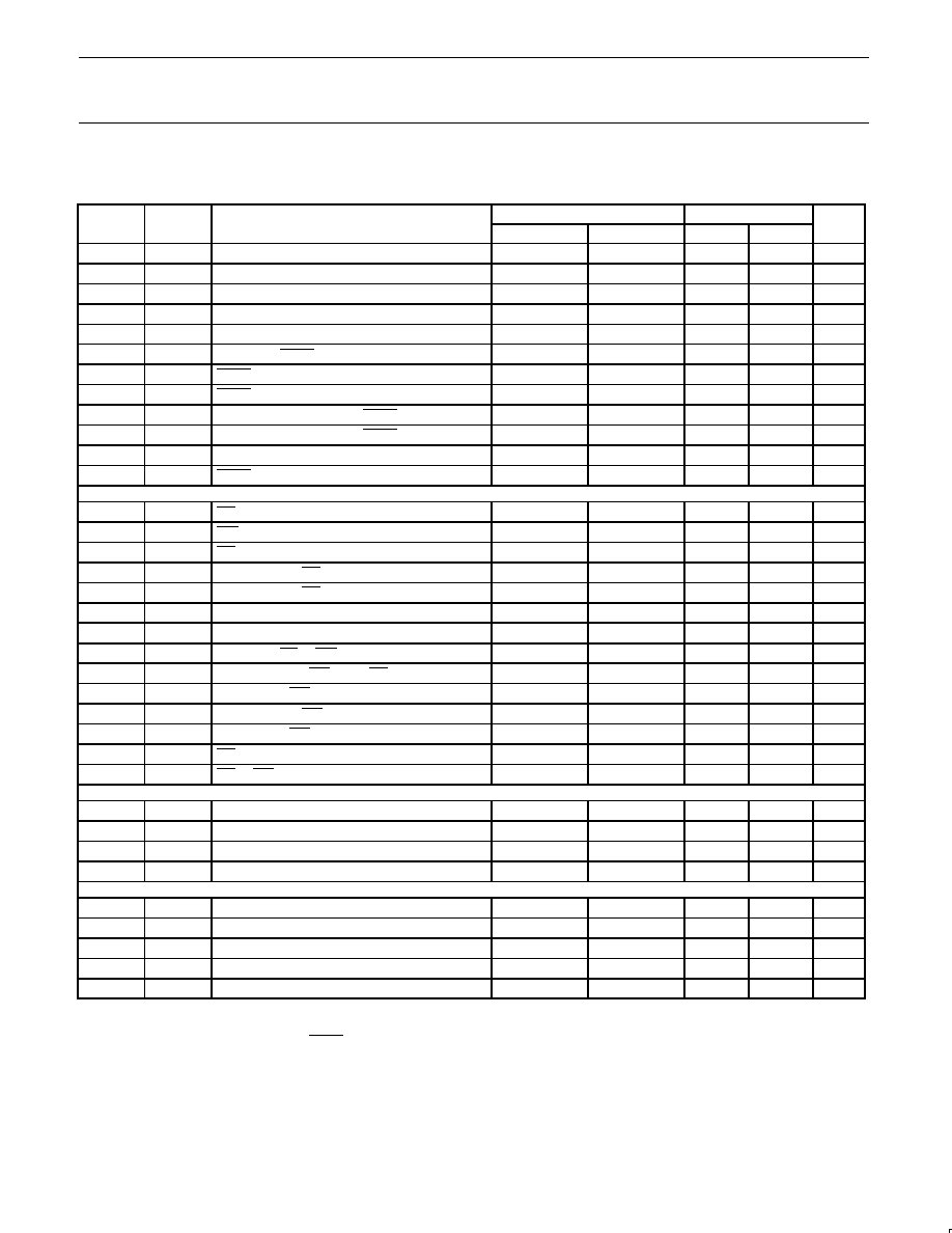
Philips Semiconductors
Product data
P80C3xX2; P80C5xX2;
P87C5xX2
80C51 8-bit microcontroller family
4K/8K/16K/32K ROM/OTP, low voltage (2.7 to 5.5 V),
low power, high speed (30/33 MHz)
2003 Jan 24
43
AC ELECTRICAL CHARACTERISTICS (6-CLOCK MODE, 2.7 V TO 5.5 V OPERATION)
T
amb
= 0
∞
C to +70
∞
C or ≠40
∞
C to +85
∞
C ; V
CC
=2.7 V to 5.5 V, V
SS
= 0 V
1,2,3,4,5
Symbol
Figure
Parameter
Limits
16 MHz Clock
Unit
MIN
MAX
MIN
MAX
1/t
CLCL
31
Oscillator frequency
0
16
≠
≠
MHz
t
LHLL
27
ALE pulse width
t
CLCL
≠10
≠
52.5
≠
ns
t
AVLL
27
Address valid to ALE low
0.5 t
CLCL
≠15
≠
16.25
≠
ns
t
LLAX
27
Address hold after ALE low
0.5 t
CLCL
≠25
≠
6.25
≠
ns
t
LLIV
27
ALE low to valid instruction in
≠
2 t
CLCL
≠55
≠
70
ns
t
LLPL
27
ALE low to PSEN low
0.5 t
CLCL
≠15
≠
16.25
≠
ns
t
PLPH
27
PSEN pulse width
1.5 t
CLCL
≠15
≠
78.75
≠
ns
t
PLIV
27
PSEN low to valid instruction in
≠
1.5 t
CLCL
≠55
≠
38.75
ns
t
PXIX
27
Input instruction hold after PSEN
0
≠
0
≠
ns
t
PXIZ
27
Input instruction float after PSEN
≠
0.5 t
CLCL
≠10
≠
21.25
ns
t
AVIV
27
Address to valid instruction in
≠
2.5 t
CLCL
≠50
≠
101.25
ns
t
PLAZ
27
PSEN low to address float
≠
10
≠
10
ns
Data Memory
t
RLRH
28
RD pulse width
3 t
CLCL
≠25
≠
162.5
≠
ns
t
WLWH
29
WR pulse width
3 t
CLCL
≠25
≠
162.5
≠
ns
t
RLDV
28
RD low to valid data in
≠
2.5 t
CLCL
≠50
≠
106.25
ns
t
RHDX
28
Data hold after RD
0
≠
0
≠
ns
t
RHDZ
28
Data float after RD
≠
t
CLCL
≠20
≠
42.5
ns
t
LLDV
28
ALE low to valid data in
≠
4 t
CLCL
≠55
≠
195
ns
t
AVDV
28
Address to valid data in
≠
4.5 t
CLCL
≠50
≠
231.25
ns
t
LLWL
28, 29
ALE low to RD or WR low
1.5 t
CLCL
≠20
1.5 t
CLCL
+20
73.75
113.75
ns
t
AVWL
28, 29
Address valid to WR low or RD low
2 t
CLCL
≠20
≠
105
≠
ns
t
QVWX
29
Data valid to WR transition
0.5 t
CLCL
≠30
≠
1.25
≠
ns
t
WHQX
29
Data hold after WR
0.5 t
CLCL
≠20
≠
11.25
≠
ns
t
QVWH
29
Data valid to WR high
3.5 t
CLCL
≠10
≠
208.75
≠
ns
t
RLAZ
28
RD low to address float
≠
0
≠
0
ns
t
WHLH
28, 29
RD or WR high to ALE high
0.5 t
CLCL
≠15
0.5 t
CLCL
+15
16.25
46.25
ns
External Clock
t
CHCX
31
High time
0.4 t
CLCL
t
CLCL
≠ t
CLCX
≠
≠
ns
t
CLCX
31
Low time
0.4 t
CLCL
t
CLCL
≠ t
CHCX
≠
≠
ns
t
CLCH
31
Rise time
≠
5
≠
≠
ns
t
CHCL
31
Fall time
≠
5
≠
≠
ns
Shift register
t
XLXL
30
Serial port clock cycle time
6 t
CLCL
≠
375
≠
ns
t
QVXH
30
Output data setup to clock rising edge
5 t
CLCL
≠25
≠
287.5
≠
ns
t
XHQX
30
Output data hold after clock rising edge
t
CLCL
≠15
≠
47.5
≠
ns
t
XHDX
30
Input data hold after clock rising edge
0
≠
0
≠
ns
t
XHDV
30
Clock rising edge to input data valid
≠
5 t
CLCL
≠133
≠
179.5
ns
NOTES:
1. Parameters are valid over operating temperature range unless otherwise specified.
2. Load capacitance for port 0, ALE, and PSEN=100 pF, load capacitance for all outputs = 80 pF
3. Interfacing the microcontroller to devices with float time up to 45ns is permitted. This limited bus contention will not cause damage to port 0
drivers.
4. Parts are guaranteed by design to operate down to 0 Hz.
5. Data shown in the table are the best mathematical models for the set of measured values obtained in tests. If a particular parameter
calculated at a customer specified frequency has a negative value, it should be considered equal to zero.

Philips Semiconductors
Product data
P80C3xX2; P80C5xX2;
P87C5xX2
80C51 8-bit microcontroller family
4K/8K/16K/32K ROM/OTP, low voltage (2.7 to 5.5 V),
low power, high speed (30/33 MHz)
2003 Jan 24
44
EXPLANATION OF THE AC SYMBOLS
Each timing symbol has five characters. The first character is always
`t' (= time). The other characters, depending on their positions,
indicate the name of a signal or the logical status of that signal. The
designations are:
A ≠ Address
C ≠ Clock
D ≠ Input data
H ≠ Logic level high
I ≠ Instruction (program memory contents)
L ≠ Logic level low, or ALE
P ≠ PSEN
Q ≠ Output data
R ≠ RD signal
t ≠ Time
V ≠ Valid
W ≠ WR signal
X ≠ No longer a valid logic level
Z ≠ Float
Examples: t
AVLL
= Time for address valid to ALE low.
t
LLPL
=Time for ALE low to PSEN low.
t
PXIZ
ALE
PSEN
PORT 0
PORT 2
A0≠A15
A8≠A15
A0≠A7
A0≠A7
t
AVLL
t
PXIX
t
LLAX
INSTR IN
t
LHLL
t
PLPH
t
LLIV
t
PLAZ
t
LLPL
t
AVIV
SU00006
t
PLIV
Figure 27. External Program Memory Read Cycle
ALE
PSEN
PORT 0
PORT 2
RD
A0≠A7
FROM RI OR DPL
DATA IN
A0≠A7 FROM PCL
INSTR IN
P2.0≠P2.7 OR A8≠A15 FROM DPF
A0≠A15 FROM PCH
t
WHLH
t
LLDV
t
LLWL
t
RLRH
t
LLAX
t
RLAZ
t
AVLL
t
RHDX
t
RHDZ
t
AVWL
t
AVDV
t
RLDV
SU00025
Figure 28. External Data Memory Read Cycle

Philips Semiconductors
Product data
P80C3xX2; P80C5xX2;
P87C5xX2
80C51 8-bit microcontroller family
4K/8K/16K/32K ROM/OTP, low voltage (2.7 to 5.5 V),
low power, high speed (30/33 MHz)
2003 Jan 24
45
t
LLAX
ALE
PSEN
PORT 0
PORT 2
WR
A0≠A7
FROM RI OR DPL
DATA OUT
A0≠A7 FROM PCL
INSTR IN
P2.0≠P2.7 OR A8≠A15 FROM DPF
A0≠A15 FROM PCH
t
WHLH
t
LLWL
t
WLWH
t
AVLL
t
AVWL
t
QVWX
t
WHQX
t
QVWH
SU00026
Figure 29. External Data Memory Write Cycle
0
1
2
3
4
5
6
7
8
INSTRUCTION
ALE
CLOCK
OUTPUT DATA
WRITE TO SBUF
INPUT DATA
CLEAR RI
SET TI
SET RI
t
XLXL
t
QVXH
t
XHQX
t
XHDX
t
XHDV
SU00027
1
2
3
0
4
5
6
7
VALID
VALID
VALID
VALID
VALID
VALID
VALID
VALID
Figure 30. Shift Register Mode Timing
VCC≠0.5
0.45V
0.7VCC
0.2VCC≠0.1
t
CHCL
t
CLCL
t
CLCH
t
CLCX
t
CHCX
SU00009
Figure 31. External Clock Drive
Philips Semiconductors
Product data
P80C3xX2; P80C5xX2;
P87C5xX2
80C51 8-bit microcontroller family
4K/8K/16K/32K ROM/OTP, low voltage (2.7 to 5.5 V),
low power, high speed (30/33 MHz)
2003 Jan 24
46
VCC≠0.5
0.45V
0.2VCC+0.9
0.2VCC≠0.1
NOTE:
AC inputs during testing are driven at V
CC
≠0.5 for a logic `1' and 0.45V for a logic `0'.
Timing measurements are made at V
IH
min for a logic `1' and V
IL
max for a logic `0'.
SU00717
Figure 32. AC Testing Input/Output
VLOAD
VLOAD+0.1V
VLOAD≠0.1V
VOH≠0.1V
VOL+0.1V
NOTE:
TIMING
REFERENCE
POINTS
For timing purposes, a port is no longer floating when a 100mV change from
load voltage occurs, and begins to float when a 100mV change from the loaded
V
OH
/V
OL
level occurs. I
OH
/I
OL
±
20mA.
SU00718
Figure 33. Float Waveform
SU01486
TYP ACTIVE MODE
MAX IDLE MODE
TYP IDLE MODE
5
4
8
12
16
FREQ AT XTAL1 (MHz)
20
24
28
32
36
15
25
I CC
(mA)
10
20
MAX ACTIVE MODE
I
CC
MAX = 0.9
FREQ. + 1.0
35
30
Figure 34. I
CC
vs. FREQ for 12-clock operation
Valid only within frequency specifications of the specified operating voltage

Philips Semiconductors
Product data
P80C3xX2; P80C5xX2;
P87C5xX2
80C51 8-bit microcontroller family
4K/8K/16K/32K ROM/OTP, low voltage (2.7 to 5.5 V),
low power, high speed (30/33 MHz)
2003 Jan 24
47
/*
## as31 version V2.10
/ *js* /
##
##
## source file: idd_ljmp1.asm
## list file: idd_ljmp1.lst created Fri Apr 20 15:51:40 2001
##
##########################################################
#0000 # AUXR equ 08Eh
#0000 # CKCON equ 08Fh
#
#
#0000 # org 0
#
# LJMP_LABEL:
0000 /75;/8E;/01; # MOV AUXR,#001h ; turn off ALE
0003 /02;/FF;/FD; # LJMP LJMP_LABEL ; jump to end of address space
0005 /00; # NOP
#
#FFFD # org 0fffdh
#
# LJMP_LABEL:
#
FFFD /02;/FD;FF; # LJMP LJMP_LABEL
# ; NOP
#
#
*/"
SU01499
Figure 35. Source code used in measuring I
DD
operational
Philips Semiconductors
Product data
P80C3xX2; P80C5xX2;
P87C5xX2
80C51 8-bit microcontroller family
4K/8K/16K/32K ROM/OTP, low voltage (2.7 to 5.5 V),
low power, high speed (30/33 MHz)
2003 Jan 24
48
V
CC
P0
EA
RST
XTAL1
XTAL2
V
SS
V
CC
V
CC
V
CC
I
CC
(NC)
CLOCK SIGNAL
SU00719
Figure 36. I
CC
Test Condition, Active Mode
All other pins are disconnected
V
CC
P0
EA
RST
XTAL1
XTAL2
V
SS
V
CC
V
CC
I
CC
(NC)
CLOCK SIGNAL
SU00720
Figure 37. I
CC
Test Condition, Idle Mode
All other pins are disconnected
VCC≠0.5
0.45V
0.7VCC
0.2VCC≠0.1
t
CHCL
t
CLCL
t
CLCH
t
CLCX
t
CHCX
SU00009
Figure 38. Clock Signal Waveform for I
CC
Tests in Active and Idle Modes
t
CLCH
= t
CHCL
= 5ns
V
CC
P0
EA
RST
XTAL1
XTAL2
VSS
V
CC
V
CC
I
CC
(NC)
SU00016
Figure 39. I
CC
Test Condition, Power Down Mode
All other pins are disconnected. V
CC
= 2 V to 5.5 V

Philips Semiconductors
Product data
P80C3xX2; P80C5xX2;
P87C5xX2
80C51 8-bit microcontroller family
4K/8K/16K/32K ROM/OTP, low voltage (2.7 to 5.5 V),
low power, high speed (30/33 MHz)
2003 Jan 24
49
EPROM CHARACTERISTICS
The OTP devices described in this data sheet can be programmed
by using a modified Improved Quick-Pulse Programming
TM
algorithm. It differs from older methods in the value used for V
PP
(programming supply voltage) and in the width and number of the
ALE/PROG pulses.
The family contains two signature bytes that can be read and used
by an EPROM programming system to identify the device. The
signature bytes identify the device as being manufactured by
Philips.
Table 9 shows the logic levels for reading the signature byte, and for
programming the program memory, the encryption table, and the
security bits. The circuit configuration and waveforms for quick-pulse
programming are shown in Figures 40 and 41. Figure 42 shows the
circuit configuration for normal program memory verification.
Quick-Pulse Programming
The setup for microcontroller quick-pulse programming is shown in
Figure 40. Note that the device is running with a 4 to 6 MHz
oscillator. The reason the oscillator needs to be running is that the
device is executing internal address and program data transfers.
The address of the EPROM location to be programmed is applied to
ports 1 and 2, as shown in Figure 40. The code byte to be
programmed into that location is applied to port 0. RST, PSEN and
pins of ports 2 and 3 specified in Table 9 are held at the `Program
Code Data' levels indicated in Table 9. The ALE/PROG is pulsed
low 5 times as shown in Figure 41.
To program the encryption table, repeat the 5 pulse programming
sequence for addresses 0 through 1FH, using the `Pgm Encryption
Table' levels. Do not forget that after the encryption table is
programmed, verification cycles will produce only encrypted data.
To program the security bits, repeat the 5 pulse programming
sequence using the `Pgm Security Bit' levels. After one security bit is
programmed, further programming of the code memory and
encryption table is disabled. However, the other security bits can still
be programmed.
Note that the EA/V
PP
pin must not be allowed to go above the
maximum specified V
PP
level for any amount of time. Even a narrow
glitch above that voltage can cause permanent damage to the
device. The V
PP
source should be well regulated and free of glitches
and overshoot.
Program Verification
If security bits 2 and 3 have not been programmed, the on-chip
program memory can be read out for program verification. The
address of the program memory locations to be read is applied to
ports 1 and 2 as shown in Figure 42. The other pins are held at the
`Verify Code Data' levels indicated in Table 9. The contents of the
address location will be emitted on port 0. External pull-ups are
required on port 0 for this operation.
If the 64 byte encryption table has been programmed, the data
presented at port 0 will be the exclusive NOR of the program byte
with one of the encryption bytes. The user will have to know the
encryption table contents in order to correctly decode the verification
data. The encryption table itself cannot be read out.
Reading the Signature bytes
The signature bytes are read by the same procedure as a normal
verification of locations 030h and 031h, except that P3.6 and P3.7
need to be pulled to a logic low. The values are:
(030h) =
15h; indicates manufacturer (Philips)
(031h) =
92h/97h/BBh/BDh; indicates P87C51X2/52X2/54X2/
58X2.
Program/Verify Algorithms
Any algorithm in agreement with the conditions listed in Table 9, and
which satisfies the timing specifications, is suitable.
Security Bits
With none of the security bits programmed the code in the program
memory can be verified. If the encryption table is programmed, the
code will be encrypted when verified. When only security bit 1 (see
Table 10) is programmed, MOVC instructions executed from
external program memory are disabled from fetching code bytes
from the internal memory, EA is latched on Reset and all further
programming of the EPROM is disabled. When security bits 1 and 2
are programmed, in addition to the above, verify mode is disabled.
When all three security bits are programmed, all of the conditions
above apply and all external program memory execution is disabled.
Encryption Array
64 bytes of encryption array are initially unprogrammed (all 1s).
TM
Trademark phrase of Intel Corporation.
Philips Semiconductors
Product data
P80C3xX2; P80C5xX2;
P87C5xX2
80C51 8-bit microcontroller family
4K/8K/16K/32K ROM/OTP, low voltage (2.7 to 5.5 V),
low power, high speed (30/33 MHz)
2003 Jan 24
50
Table 9. EPROM Programming Modes
MODE
RST
PSEN
ALE/PROG
EA/V
PP
P2.7
P2.6
P3.7
P3.6
P3.3
Read signature
1
0
1
1
0
0
0
0
X
Program code data
1
0
0*
V
PP
1
0
1
1
X
Verify code data
1
0
1
1
0
0
1
1
X
Pgm encryption table
1
0
0*
V
PP
1
0
1
0
X
Pgm security bit 1
1
0
0*
V
PP
1
1
1
1
X
Pgm security bit 2
1
0
0*
V
PP
1
1
0
0
X
Pgm security bit 3
1
0
0*
V
PP
0
1
0
1
X
Program to 6-clock mode
1
0
0*
V
PP
0
0
1
0
0
Verify 6-clock
4
1
0
1
1
e
0
0
1
1
Verify security bits
5
1
0
1
1
e
0
1
0
X
NOTES:
1. `0' = Valid low for that pin, `1' = valid high for that pin.
2. V
PP
= 12.75 V
±
0.25 V.
3. V
CC
= 5 V
±
10% during programming and verification.
4. Bit is output on P0.4 (1 = 12x, 0 = 6x).
5. Security bit one is output on P0.7.
Security bit two is output on P0.6.
Security bit three is output on P0.3.
*
ALE/PROG receives 5 programming pulses for code data (also for user array; 5 pulses for encryption or security bits) while V
PP
is held at
12.75 V. Each programming pulse is low for 100
µ
s (
±
10
µ
s) and high for a minimum of 10
µ
s.
Table 10. Program Security Bits for EPROM Devices
PROGRAM LOCK BITS
1, 2
SB1
SB2
SB3
PROTECTION DESCRIPTION
1
U
U
U
No Program Security features enabled. (Code verify will still be encrypted by the Encryption Array if
programmed.)
2
P
U
U
MOVC instructions executed from external program memory are disabled from fetching code bytes
from internal memory, EA is sampled and latched on Reset, and further programming of the EPROM
is disabled.
3
P
P
U
Same as 2, also verify is disabled.
4
P
P
P
Same as 3, external execution is disabled. Internal data RAM is not accessible.
NOTES:
1. P ≠ programmed. U ≠ unprogrammed.
2. Any other combination of the security bits is not defined.
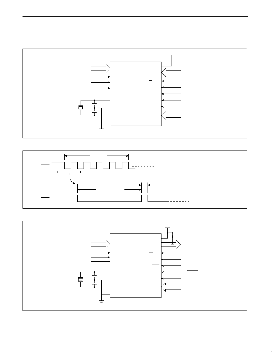
Philips Semiconductors
Product data
P80C3xX2; P80C5xX2;
P87C5xX2
80C51 8-bit microcontroller family
4K/8K/16K/32K ROM/OTP, low voltage (2.7 to 5.5 V),
low power, high speed (30/33 MHz)
2003 Jan 24
51
A0≠A7
1
1
1
4≠6MHz
+5V
PGM DATA
+12.75V
5 PULSES TO GROUND
0
1
0
A8≠A12
P1
RST
P3.6
P3.7
XTAL2
XTAL1
VSS
VCC
P0
EA/VPP
ALE/PROG
PSEN
P2.7
P2.6
P2.0≠P2.5
OTP
SU01488
Figure 40. Programming Configuration
ALE/PROG:
ALE/PROG:
1
0
1
0
5 PULSES
t
GLGH
= 100
µ
s
±
10
µ
s
t
GHGL
= 10
µ
s MIN
SU00875
1
2
3
4
5
SEE EXPLODED VIEW BELOW
1
Figure 41. PROG Waveform
A0≠A7
1
1
1
+5V
PGM DATA
1
1
0
0 ENABLE
0
A8≠A12
P1
RST
P3.6
P3.7
XTAL2
XTAL1
VSS
VCC
P0
EA/VPP
ALE/PROG
PSEN
P2.7
P2.6
P2.0≠P2.5
OTP
SU01489
4≠6MHz
Figure 42. Program Verification
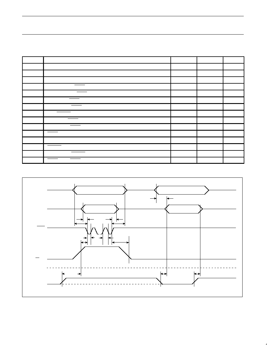
Philips Semiconductors
Product data
P80C3xX2; P80C5xX2;
P87C5xX2
80C51 8-bit microcontroller family
4K/8K/16K/32K ROM/OTP, low voltage (2.7 to 5.5 V),
low power, high speed (30/33 MHz)
2003 Jan 24
52
PROGRAMMING AND VERIFICATION CHARACTERISTICS
T
amb
= 21
∞
C to +27
∞
C, V
CC
= 5 V
±
10%, V
SS
= 0 V (See Figure 43)
SYMBOL
PARAMETER
MIN
MAX
UNIT
V
PP
Programming supply voltage
12.5
13.0
V
I
PP
Programming supply current
50
1
mA
1/t
CLCL
Oscillator frequency
4
6
MHz
t
AVGL
Address setup to PROG low
48t
CLCL
t
GHAX
Address hold after PROG
48t
CLCL
t
DVGL
Data setup to PROG low
48t
CLCL
t
GHDX
Data hold after PROG
48t
CLCL
t
EHSH
P2.7 (ENABLE) high to V
PP
48t
CLCL
t
SHGL
V
PP
setup to PROG low
10
µ
s
t
GHSL
V
PP
hold after PROG
10
µ
s
t
GLGH
PROG width
90
110
µ
s
t
AVQV
Address to data valid
48t
CLCL
t
ELQZ
ENABLE low to data valid
48t
CLCL
t
EHQZ
Data float after ENABLE
0
48t
CLCL
t
GHGL
PROG high to PROG low
10
µ
s
NOTE:
1. Not tested.
PROGRAMMING
*
VERIFICATION
*
ADDRESS
ADDRESS
DATA IN
DATA OUT
LOGIC 1
LOGIC 1
LOGIC 0
t
AVQV
t
EHQZ
t
ELQV
t
SHGL
t
GHSL
t
GLGH
t
GHGL
t
AVGL
t
GHAX
t
DVGL
t
GHDX
P1.0≠P1.7
P2.0≠P2.5
P3.4
(A0 ≠ A12)
PORT 0
P0.0 ≠ P0.7
(D0 ≠ D7)
ALE/PROG
EA/V
PP
P2.7
**
SU01414
t
EHSH
NOTES:
*
FOR PROGRAMMING CONFIGURATION SEE FIGURE 40.
FOR VERIFICATION CONDITIONS SEE FIGURE 42.
**
SEE TABLE 9.
Figure 43. Programming and Verification
Philips Semiconductors
Product data
P80C3xX2; P80C5xX2;
P87C5xX2
80C51 8-bit microcontroller family
4K/8K/16K/32K ROM/OTP, low voltage (2.7 to 5.5 V),
low power, high speed (30/33 MHz)
2003 Jan 24
53
MASK ROM DEVICES
Security Bits
With none of the security bits programmed the code in the program
memory can be verified. If the encryption table is programmed, the
code will be encrypted when verified. When only security bit 1 (see
Table 11) is programmed, MOVC instructions executed from external
program memory are disabled from fetching code bytes from the
internal memory, EA is latched on Reset and all further programming
of the EPROM is disabled. When security bits 1 and 2 are
programmed, in addition to the above, verify mode is disabled.
Encryption Array
64 bytes (87C51), or 32 bytes (87C52/4) of encryption array are
initially unprogrammed (all 1s).
Table 11. Program Security Bits
PROGRAM LOCK BITS
1, 2
SB1
SB2
PROTECTION DESCRIPTION
1
U
U
No Program Security features enabled.
(Code verify will still be encrypted by the Encryption Array if programmed.)
2
P
U
MOVC instructions executed from external program memory are disabled from fetching code bytes from
internal memory, EA is sampled and latched on Reset, and further programming of the EPROM is disabled.
NOTES:
1. P ≠ programmed. U ≠ unprogrammed.
2. Any other combination of the security bits is not defined.
80C51X2 ROM CODE SUBMISSION
When submitting a ROM code for the 80C51X2, the following must be specified:
1. 4 kbyte user ROM data
2. 64 byte ROM encryption key
3. ROM security bits.
ADDRESS
CONTENT
BIT(S)
COMMENT
0000H to 0FFFH
DATA
7:0
User ROM Data
1000H to 103FH
KEY
7:0
ROM Encryption Key
1040H
SEC
0
ROM Security Bit 1
1040H
SEC
1
ROM Security Bit 2
Security Bit 1:
When programmed, this bit has two effects on masked ROM parts:
1. External MOVC is disabled, and
2. EA is latched on Reset.
Security Bit 2:
When programmed, this bit inhibits Verify User ROM.
NOTE: Security Bit 2 cannot be enabled unless Security Bit 1 is enabled.
If the ROM Code file does not include the options, the following information must be included with the ROM code.
For each of the following, check the appropriate box, and send to Philips along with the code:
Security Bit #1:
V
Enabled
V
Disabled
Security Bit #2:
V
Enabled
V
Disabled
Encryption:
V
No
V
Yes
If Yes, must send key file.
80C52X2 ROM CODE SUBMISSION
When submitting a ROM code for the 80C52X2, the following must be specified:
1. 8 kbyte user ROM data
2. 64 byte ROM encryption key
3. ROM security bits.
Philips Semiconductors
Product data
P80C3xX2; P80C5xX2;
P87C5xX2
80C51 8-bit microcontroller family
4K/8K/16K/32K ROM/OTP, low voltage (2.7 to 5.5 V),
low power, high speed (30/33 MHz)
2003 Jan 24
54
ADDRESS
CONTENT
BIT(S)
COMMENT
0000H to 1FFFH
DATA
7:0
User ROM Data
2000H to 203FH
KEY
7:0
ROM Encryption Key
2040H
SEC
0
ROM Security Bit 1
2040H
SEC
1
ROM Security Bit 2
Security Bit 1:
When programmed, this bit has two effects on masked ROM parts:
1. External MOVC is disabled, and
2. EA is latched on Reset.
Security Bit 2:
When programmed, this bit inhibits Verify User ROM.
NOTE: Security Bit 2 cannot be enabled unless Security Bit 1 is enabled.
If the ROM Code file does not include the options, the following information must be included with the ROM code.
For each of the following, check the appropriate box, and send to Philips along with the code:
Security Bit #1:
V
Enabled
V
Disabled
Security Bit #2:
V
Enabled
V
Disabled
Encryption:
V
No
V
Yes
If Yes, must send key file.

Philips Semiconductors
Product data
P80C3xX2; P80C5xX2;
P87C5xX2
80C51 8-bit microcontroller family
4K/8K/16K/32K ROM/OTP, low voltage (2.7 to 5.5 V),
low power, high speed (30/33 MHz)
2003 Jan 24
55
80C54X2 ROM CODE SUBMISSION
When submitting a ROM code for the 80C54X2, the following must be specified:
1. 16 kbyte user ROM data
2. 64 byte ROM encryption key
3. ROM security bits.
ADDRESS
CONTENT
BIT(S)
COMMENT
0000H to 3FFFH
DATA
7:0
User ROM Data
4000H to 403FH
KEY
7:0
ROM Encryption Key
FFH = no encryption
4040H
SEC
0
ROM Security Bit 1
0 = enable security
1 = disable security
4040H
SEC
1
ROM Security Bit 2
0 = enable security
1 = disable security
Security Bit 1: When programmed, this bit has two effects on masked ROM parts:
1. External MOVC is disabled, and
2. EA is latched on Reset.
Security Bit 2: When programmed, this bit inhibits Verify User ROM.
NOTE: Security Bit 2 cannot be enabled unless Security Bit 1 is enabled.
If the ROM Code file does not include the options, the following information must be included with the ROM code.
For each of the following, check the appropriate box, and send to Philips along with the code:
Security Bit #1:
V
Enabled
V
Disabled
Security Bit #2:
V
Enabled
V
Disabled
Encryption:
V
No
V
Yes
If Yes, must send key file.
Philips Semiconductors
Product data
P80C3xX2; P80C5xX2;
P87C5xX2
80C51 8-bit microcontroller family
4K/8K/16K/32K ROM/OTP, low voltage (2.7 to 5.5 V),
low power, high speed (30/33 MHz)
2003 Jan 24
56
80C58X2 ROM CODE SUBMISSION
When submitting a ROM code for the 80C58X2, the following must be specified:
1. 32 kbyte user ROM data
2. 64 byte ROM encryption key
3. ROM security bits.
ADDRESS
CONTENT
BIT(S)
COMMENT
0000H to 7FFFH
DATA
7:0
User ROM Data
8000H to 803FH
KEY
7:0
ROM Encryption Key
FFH = no encryption
8040H
SEC
0
ROM Security Bit 1
0 = enable security
1 = disable security
8040H
SEC
1
ROM Security Bit 2
0 = enable security
1 = disable security
Security Bit 1: When programmed, this bit has two effects on masked ROM parts:
1. External MOVC is disabled, and
2. EA is latched on Reset.
Security Bit 2: When programmed, this bit inhibits Verify User ROM.
NOTE: Security Bit 2 cannot be enabled unless Security Bit 1 is enabled.
If the ROM Code file does not include the options, the following information must be included with the ROM code.
For each of the following, check the appropriate box, and send to Philips along with the code:
Security Bit #1:
V
Enabled
V
Disabled
Security Bit #2:
V
Enabled
V
Disabled
Encryption:
V
No
V
Yes
If Yes, must send key file.
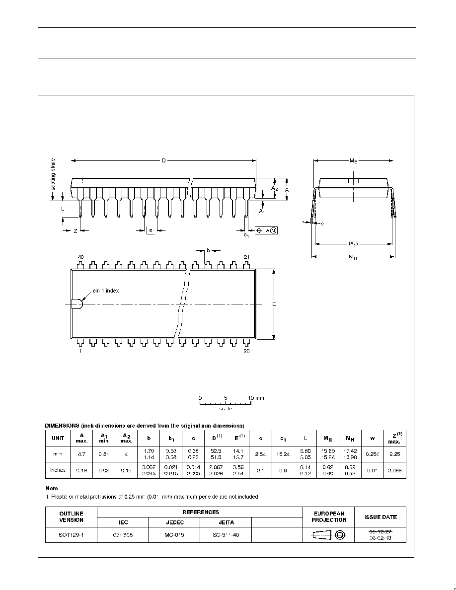
Philips Semiconductors
Product data
P80C3xX2; P80C5xX2;
P87C5xX2
80C51 8-bit microcontroller family
4K/8K/16K/32K ROM/OTP, low voltage (2.7 to 5.5 V),
low power, high speed (30/33 MHz)
2003 Jan 24
57
DIP40:
plastic dual in-line package; 40 leads (600 mil)
SOT129-1

Philips Semiconductors
Product data
P80C3xX2; P80C5xX2;
P87C5xX2
80C51 8-bit microcontroller family
4K/8K/16K/32K ROM/OTP, low voltage (2.7 to 5.5 V),
low power, high speed (30/33 MHz)
2003 Jan 24
58
PLCC44:
plastic leaded chip carrier; 44 leads
SOT187-2
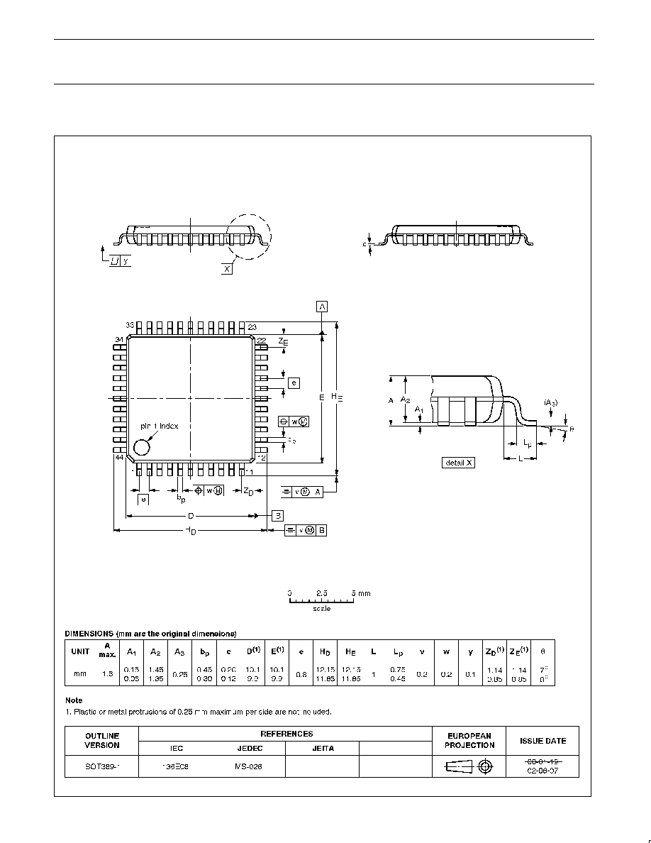
Philips Semiconductors
Product data
P80C3xX2; P80C5xX2;
P87C5xX2
80C51 8-bit microcontroller family
4K/8K/16K/32K ROM/OTP, low voltage (2.7 to 5.5 V),
low power, high speed (30/33 MHz)
2003 Jan 24
59
LQFP44:
plastic low profile quad flat package; 44 leads; body 10 x 10 x 1.4 mm
SOT389-1

Philips Semiconductors
Product data
P80C3xX2; P80C5xX2;
P87C5xX2
80C51 8-bit microcontroller family
4K/8K/16K/32K ROM/OTP, low voltage (2.7 to 5.5 V),
low power, high speed (30/33 MHz)
2003 Jan 24
60
TSSOP38:
plastic thin shrink small outline package; 38 leads;
body width 4.4 mm; lead pitch 0.5 mm
SOT510-1
Philips Semiconductors
Product data
P80C3xX2; P80C5xX2;
P87C5xX2
80C51 8-bit microcontroller family
4K/8K/16K/32K ROM/OTP, low voltage (2.7 to 5.5 V),
low power, high speed (30/33 MHz)
2003 Jan 24
61
REVISION HISTORY
Rev
Date
Description
_6
20030124
Product data (9397 750 10995); ECN 853-2337 29260 of 06 December 2002
Modifications:
∑
Added TSSOP38 package details
_5
20020912
Product data (9397 750 10361); ECN 853-2337 28906 of 12 September 2002
_4
20020612
Product data (9397 750 09969); ECN 853-2337 28427 of 12 June 2002
_3
20020422
Product data (9397 750 09779); ECN 853-2337 28059 of 22 April 2002
_2
20020219
Preliminary data (9397 750 09467)
_1
20010924
Preliminary data (9397 750 08895); initial release

Philips Semiconductors
Product data
P80C3xX2; P80C5xX2;
P87C5xX2
80C51 8-bit microcontroller family
4K/8K/16K/32K ROM/OTP, low voltage (2.7 to 5.5 V),
low power, high speed (30/33 MHz)
2003 Jan 24
62
Definitions
Short-form specification -- The data in a short-form specification is extracted from a full data sheet with the same type number and title. For detailed information see
the relevant data sheet or data handbook.
Limiting values definition -- Limiting values given are in accordance with the Absolute Maximum Rating System (IEC 60134). Stress above one or more of the limiting
values may cause permanent damage to the device. These are stress ratings only and operation of the device at these or at any other conditions above those given
in the Characteristics sections of the specification is not implied. Exposure to limiting values for extended periods may affect device reliability.
Application information -- Applications that are described herein for any of these products are for illustrative purposes only. Philips Semiconductors make no
representation or warranty that such applications will be suitable for the specified use without further testing or modification.
Disclaimers
Life support -- These products are not designed for use in life support appliances, devices, or systems where malfunction of these products can reasonably be
expected to result in personal injury. Philips Semiconductors customers using or selling these products for use in such applications do so at their own risk and agree
to fully indemnify Philips Semiconductors for any damages resulting from such application.
Right to make changes -- Philips Semiconductors reserves the right to make changes in the products--including circuits, standard cells, and/or software--described
or contained herein in order to improve design and/or performance. When the product is in full production (status `Production'), relevant changes will be communicated
via a Customer Product/Process Change Notification (CPCN). Philips Semiconductors assumes no responsibility or liability for the use of any of these products, conveys
no license or title under any patent, copyright, or mask work right to these products, and makes no representations or warranties that these products are free from patent,
copyright, or mask work right infringement, unless otherwise specified.
Contact information
For additional information please visit
http://www.semiconductors.philips.com.
Fax: +31 40 27 24825
For sales offices addresses send e-mail to:
sales.addresses@www.semiconductors.philips.com.
©
Koninklijke Philips Electronics N.V. 2003
All rights reserved. Printed in U.S.A.
Date of release: 01≠03
Document order number:
9397 750 10995
Philips
Semiconductors
Data sheet status
[1]
Objective data
Preliminary data
Product data
Product
status
[2] [3]
Development
Qualification
Production
Definitions
This data sheet contains data from the objective specification for product development.
Philips Semiconductors reserves the right to change the specification in any manner without notice.
This data sheet contains data from the preliminary specification. Supplementary data will be published
at a later date. Philips Semiconductors reserves the right to change the specification without notice, in
order to improve the design and supply the best possible product.
This data sheet contains data from the product specification. Philips Semiconductors reserves the
right to make changes at any time in order to improve the design, manufacturing and supply. Relevant
changes will be communicated via a Customer Product/Process Change Notification (CPCN).
Data sheet status
[1] Please consult the most recently issued data sheet before initiating or completing a design.
[2] The product status of the device(s) described in this data sheet may have changed since this data sheet was published. The latest information is available on the Internet at URL
http://www.semiconductors.philips.com.
[3] For data sheets describing multiple type numbers, the highest-level product status determines the data sheet status.
Level
I
II
III