 | –≠–ª–µ–∫—Ç—Ä–æ–Ω–Ω—ã–π –∫–æ–º–ø–æ–Ω–µ–Ω—Ç: 80CL31 | –°–∫–∞—á–∞—Ç—å:  PDF PDF  ZIP ZIP |
Philips
Semiconductors
80CL31/80CL51
Low-voltage single-chip
8-bit microcontrollers
Product specification
1995 January
INTEGRATED CIRCUITS
IC20 Data Handbook
Philips Semiconductors
Product specification
80CL31/80CL51
Low-voltage single-chip 8-bit microcontrollers
2
January 1995
FEATURES
∑
Full static 80C51 CPU
∑
8-bit CPU, ROM, RAM, 1/0 in a single 40-lead DIL / mini-pack
∑
4K x 8 ROM, expandable externally to 64K bytes
∑
128 bytes RAM, expandable externally to 64K bytes
∑
Four 8-bit ports, 321/0 lines
∑
Two 16-bit timer / event counters
∑
External memory expandable up to 128K, external ROM up to
64K and / or RAM up to 64K
∑
On-chip oscillator suitable for RC, LC, quartz crystal or ceramic
resonator
∑
Thirteen source, thirteen vector interrupt structure with two priority
levels
∑
Full duplex serial port (UART)
∑
Enhanced architecture with:
≠ non-page oriented instructions
≠ direct addressing
≠ four eight byte RAM register banks
≠ stack depth up to 128 bytes
≠ multiply, divide, subtract and compare instructions
∑
Power-Down and IDLE instructions
∑
Wake-up via external interrupts at Port 1
∑
Single supply voltage of 1.8V to 6.0V (5.0V
±
10% for P80C51)
∑
Frequency range of 0 to 16MHz (3.5MHz to 16MHz for P80C51)
∑
Very low current consumption
∑
Operating temperature range:
-40 to +85
o
C
DESCRIPTION
The 80CL51 is manufactured in an advanced CMOS technology.
The instruction set of the 80CL51 is based on that of the 8051. The
80CL51 is a general purpose microcontroller especially suited for
battery-powered applications. The device has low power
consumption and a wide range of supply voltage. For emulation
purposes, the 85CL000 (Piggy-back version) with 256 bytes of RAM
is recommended. The 80CL51 has two software selectable modes
of reduced activity for further power reduction: Idle and Power-down.
The 80CL51 also functions as an arithmetic processor having
facilities for both binary and BCD arithmetic plus bit-handling
capabilities. The instruction set consists of over 100 instructions: 49
one-byte, 46 two-byte, and 16 three-byte.
The P80CL31 is the ROMless version of the P80CL51. P80C51 is a
5V version of the low voltage P80CL51.
The P80CL31 is the ROMless version of the P80CL51. P80C51 is a
5V version of the low voltage P80CL51.
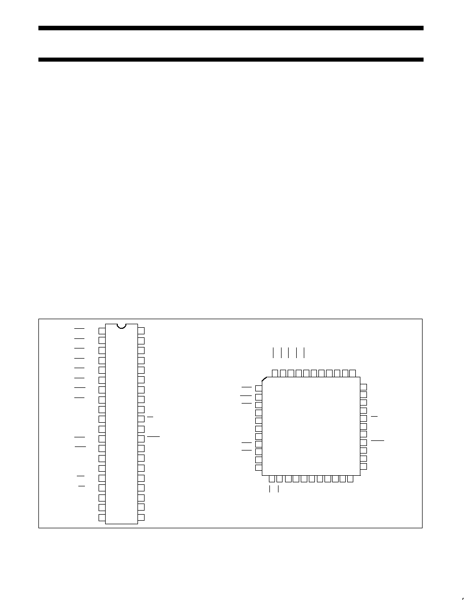
PIN CONFIGURATIONS
PLASTIC QUAD FLAT PACKAGE
P3.6/WR
P3.7/RD
XT
AL2
XT
AL1
V
P2.0/A8
P2.1/A9
P2.2/A10
P2.3/A1
1
P2.4/A12
NC
SS
P1.4/INT6
P1.3/INT5
P1.2/INT4
P1.1/INT3
P1.0/INT2
NC
P0.0/AD0
P0.1/AD1
P0.2/AD2
P0.3/AD3
V
DD
39 38 37 36 35 34
33
32
31
30
29
28
27
26
25
24
23
22
21
40
41
42
43
44
1
2
3
4
5
6
7
8
9
10
11
12 13 14 15 16 17 18 19 20
P1.5/INT7
P1.6/INT8
P1.7/INT9
RST
P3.0/RXD
NC
P3.1/TXD
P3.2/INT0
P3.3/INT1
P3.4/T0
P3.5/T1
P0.4/AD4
P0.5/AD5
P0.6/AD6
P0.7/AD7
EA
ALE
PSEN
P2.7/A15
P2.6/A14
P2.5/A13
NC
1
2
3
4
5
6
7
8
9
10
11
12
13
14
15
16
17
18
19
20
21
22
23
24
25
26
27
28
29
30
31
32
33
34
35
36
37
38
39
40
INT2/P1.0
RST
RXD/DATA/P3.0
TXD/CLOCK/P3.1
INT0/P3.2
INT1/P3.3
T0/P3.4
T1/P3.5
WR/P3.6
RD/P3.7
XTAL2
XTAL1
VSS
P2.0/A8
P2.1/A9
P2.2/A10
P2.3/A11
P2.4/A12
P2.5/A13
P2.6/A14
P2.7/A15
PSEN
ALE
EA
P0.7/AD7
P0.6/AD6
P0.5/AD5
P0.4/AD4
P0.3/AD3
P0.2/AD2
P0.1/AD1
P0.0/AD0
VDD
PLASTIC
DUAL
IN-LINE
AND
SMALL
OUTLINE
PACKAGES
INT3/P1.1
INT4/P1.2
INT5/P1.3
INT6/P1.4
INT7/P1.5
INT8/P1.6
INT9/P1.7
Philips Semiconductors
Product specification
80CL31/80CL51
Low-voltage single-chip 8-bit microcontrollers
January 1995
3
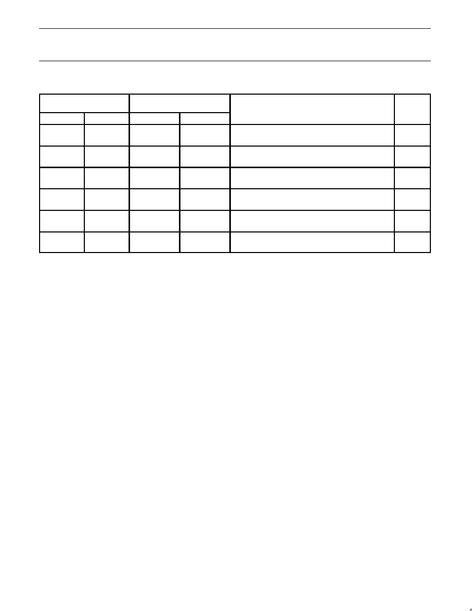
ORDERING INFORMATION
PHILIPS PART ORDER
NUMBER PART MARKING
PHILIPS NORTH AMERICA
1
PART ORDER NUMBER
TEMPERATURE RANGE
o
C
AND PACKAGE
DRAWING
NUMBER
ROMless
ROM
ROMless
ROM
AND PACKAGE
NUMBER
P80CL31HFP
P80CL51HFP
P80CL31HFP N
P80CL51HFP N
≠40 to +85;
40-lead Plastic Dual In-line Package (1.8V to 6V)
SOT129-1
P80CL31HFT
P80CL51HFT
P80CL31HFT D
P80CL51HFT D
≠40 to +85;
40-lead Plastic Small Outline Package (1.8V to 6V)
SOT158-1
P80CL31HFH
P80CL51HFH
P80CL31HFH B
P80CL51HFH B
≠40 to +85;
44-lead Plastic Quad Flat Package (1.8V to 6V)
SOT307-2
P80C51HFP
P80C51HFP N
≠40 to +85;
40-lead Plastic Dual In-line Package (5.0V
±
10%)
SOT129-1
P80C51HFT
P80C51HFT D
≠40 to +85;
40-lead Plastic Small Outline Package (5.0V
±
10%)
SOT158-1
P80C51HFH
P80C51HFH B
≠40 to +85;
44-lead Plastic Quad Flat Package (5.0V
±
10%)
SOT307-2
NOTE:
1. Parts ordered by the Philips North America part number will be marked with the Philips part marking.
Philips Semiconductors
Product specification
80CL31/80CL51
Low-voltage single-chip 8-bit microcontrollers
January 1995
4
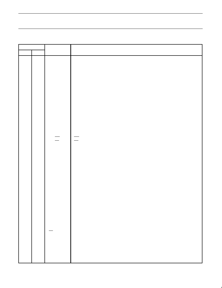
PIN DESCRIPTIONS
PIN
DESIGNATION
FUNCTION
QFP
DIP
DESIGNATION
FUNCTION
40
1
P1.O/INT2
Port 1: Port 1 is an 8-bit bidirectional I/O port with internal pullups. Port 1 pins that have 1s written
to them are pulled HIGH by the internal pullups and in that state can be used as inputs The Port 1
41
2
P1.1/lNT3
to them are pulled HIGH by the internal pullups, and in that state can be used as inputs. The Port 1
output buffer can sink/source 4 LS TTL loads As inputs Port 1 pins that are externally pulled LOW
42
3
P1.2/lNT4
output buffer can sink/source 4 LS TTL loads. As inputs, Port 1 pins that are externally pulled LOW
will source current (I
lL
in the characteristics) due to the internal pullups Port 1 also serves the
43
4
P1.3/INT5
will source current (I
lL
in the characteristics) due to the internal pullups. Port 1 also serves the
alternative functions INT2 to INT9
44
5
P1.4/lNT6
alternative functions INT2 to INT9.
1
6
P1.5/lNT7
2
7
P1.6/lNT8
3
8
P1.7/lNT9
4
9
RST
Reset: A high level on this pin for two machine cycles while the oscillator is running resets the
device.
5≠13
10-17
Port 3: Port 3 is an 8-bit bidirectional I/O port with internal pull-ups. The Port 3 output buffers can
sink/source 4 LS TTL inputs. Port 3 pins that have 1s written to them are pulled HIGH by the
internal pull ups, and in that state can be used as inputs. As inputs, Port 3 pins that are externally
pulled LOW will source current (I
lL
in the characteristics) due to the internal pull ups.
5
10
P3.0/RXD/data
RXD/data: Serial port receiver data input (asynchronous)or data input/output (synchronous)
7
11
P3.1/TXD/clock
TXD/clock: Serial port transmitter data output (asynchronous) or clock output (synchronous)
8
12
P3.2/lNT0
INT0: External interrupt 0.
9
13
P3.3/lNT1
INT1: External interrupt 1.
10
14
P3.4/T0
T0: Timer 0 external input.
11
15
P3.5/T1
T1: Timer 1 external input.
12
16
P3.6/WR
WR: External data memory write strobe.
13
17
P3.7/RD
RD: External data memory read strobe.
14
18
XTAL2
Crystal output: Output of the inverting amplifier of the oscillator. Left open when external clock is
used.
Crystal input: Input to the inverting amplifier of the oscillator; also the input for an externally gen-
erated clock source.
15
19
XTAL1
Crystal input: Input to the inverting amplifier of the oscillator; also the input for an externally
generated clock source.
16
20
Vss
Ground: Circuit ground potential.
18-25
21-28
P2.0-P2.7
Port 2: Port 2 is an 8-bit bidirectional 1/0 port with internal pullups. Port 2 pins that have 1s written
to them are pulled HIGH by the internal pullups, and in that state can be used as inputs. The Port 2
output buffer can sink/source 4 LS TTL loads.
Port 2 emits the high-order address byte during accesses to external memory that use 1 6-bit ad-
dresses (MOVX @DPTR). In this application it uses the strong internal pullups when emitting 1s.
During accesses to external memory that use 8-bit addresses (MOVX @Ri), Port 2 emits the con-
tents of the P2 Special Function Register.
26
29
PSEN
Program store enable output: Read strobe to external program memory. When executing code
out of external program memory, PSEN is activated twice each machine cycle. However, during
each access to external data memory two PSEN activations are skipped.
27
30
ALE
Address Latch Enable: Output pulse for latching the low byte of the address during access to
external memory. ALE is emitted at a constant rate of 1/6 of the oscillator frequency, and may be
used for external timing or clocking purposes.
29
31
EA
External Access: When EA is held High the CPU executes out of internal program memory (un-
less the program counter exceeds 0FFFH). Holding EA LOW forces the CPU to execute out of
external memory regardless of the value of the program counter.
30-37
32-39
P0.0-P00.7
Port 0: Port 0 is an 8-bit open drain bidirectional I/O port. As an open drain output port it can sink 8
LS TTL loads. Port 0 pins that have 1s written to them float, and in that state will function as high
impedance inputs. Port 0 is also the multiplexed low order address and data bus during access to
external memory. In this application it uses strong internal pull-ups when emitting logic 1s.
38
40
V
DD
Power supply.
Philips Semiconductors
Product specification
80CL31/80CL51
Low-voltage single-chip 8-bit microcontrollers
January 1995
5
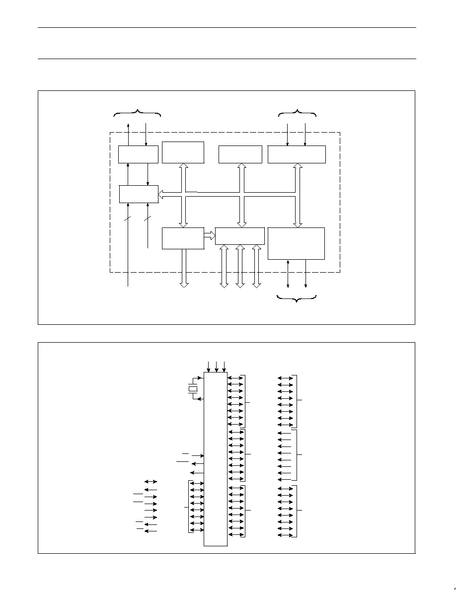
BLOCK DIAGRAM
PROGRAMMABLE
I/O
TWO 16-BIT TIMER/
EVENT COUNTERS
DATA MEMORY
(128 BY 8 RAM)
PROGRAM
MEMORY
(4K BY 8 ROM)
64K BYTE BUS
EXPANSION
CONTROL
OSCILLATOR
AND TIMING
CPU
PROGRAMMABLE
SERIAL PORT,
FULL DUPLEX UART,
SYNCHRONOUS
SHIFT
RXD
TXD
(1)
PARALLEL PORTS
ADDRESS/DATA BUS
I/O PINS
CONTROL
10
3
INTERNAL
INTERRUPTS
XTAL2 XTAL1
FREQUENNCY REFERENCE
T0
T1
COUNTER1
80CL51
EXTERNAL ENTERRUPTS1
1. Pins shared with parallels ports pins.
FUNCTIONAL DIAGRAM
PORT 0
PORT 1
PORT 2
PORT 3
ADDRESS AND
DATA BUS
ADDRESS BUS
RxD/data
TxD/clock
INT0
INT1
T0
T1
WR
RD
ALTERNATIVE
EA
PSEN
ALE
VSS
VDD
RST
INT2/INT9
XTAL1
XTAL2
FUNCTIONS