Philips Semiconductors
Product specification
80C451/83C451/87C451
80C51 8-bit microcontroller family
4K/128 OTP/ROM/ROMless, expanded I/O
2
1998 May 01
853-0830 19327
DESCRIPTION
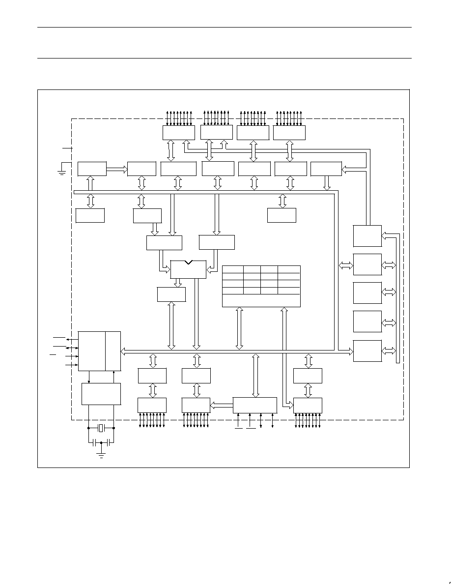
The Philips 8XC451 is an I/O expanded single-chip microcontroller
fabricated with Philips high-density CMOS technology. Philips
epitaxial substrate minimizes latch-up sensitivity.
The 8XC451 (includes the 80C451, 87C451 and 83C451) is a
functional extension of the 87C51 microcontroller with three
additional I/O ports and four I/O control lines for a total of 68 pins.
Four control lines associated with port 6 facilitate high-speed
asynchronous I/O functions.
The 8XC451 includes a 4k
�
8 ROM (83C451) EPROM (87C451), a
128
�
8 RAM, 56 I/O, two 16-bit timer/counters, a five source, two
priority level, nested interrupt structure, a serial I/O port for either a
full duplex UART, I/O expansion, or multi-processor
communications, and on-chip oscillator and clock circuits. The
80C451 ROMless version includes all of the 83C451 features except
the on-board 4k
�
8 ROM.
The 87C451 has 4k of EPROM on-chip as program memory and is
otherwise identical to the 83C451.
The 8XC451 has two software selectable modes of reduced activity
for further power reduction; idle mode and power-down mode. Idle
mode freezes the CPU while allowing the RAM, timers, serial port,
and interrupt system to continue functioning. Power-down mode
freezes the oscillator, causing all other chip functions to be
inoperative while maintaining the RAM contents.
FEATURES
�
80C51 based architecture
�
Seven 8-bit I/O ports
�
Port 6 features:
� Eight data pins
� Four control pins
� Direct MPU bus interface
� Parallel printer interface
�
On the microcontroller:
� 4k
�
8 ROM (83C451)
4k
�
8 EPROM (87C451)
ROMless version (80C451)
� 128
�
8 RAM
� Two 16-bit counter/timers
� Two external interrupts
�
External memory addressing capability
� 64k ROM and 64k RAM
�
Low power consumption:
� Normal operation: less than 24mA at 5V, 12MHz
� Idle mode
� Power-down mode
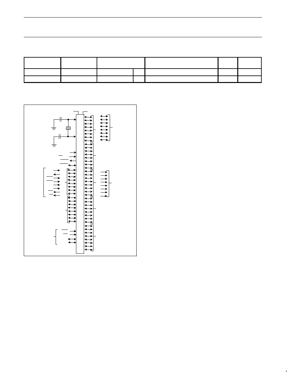
PIN CONFIGURATION
LCC
9
1
61
10
26
60
44
27
43
Pin
Function
1
EA/VPP
2
P2.0/A8
3
P2.1/A9
4
P2.2/A10
5
P2.3/A11
6
P2.4/A12
7
P2.5/A13
8
P2.6/A14
9
P2.7/A15
10
P0.7/AD7
11
P0.6/AD6
12
P0.5/AD5
13
P0.4/AD4
14
P0.3/AD3
15
P0.2/AD2
16
P0.1/AD1
17
P0.0/AD0
18
V
CC
19
P4.7
20
P4.6
21
P4.5
22
P4.4
23
P4.3
Pin
Function
24
P4.2
25
P4.1
26
P4.0
27
P1.0
28
P1.1
29
P1.2
30
P1.3
31
P1.4
32
P1.5
33
P1.6
34
P1.7
35
RST
36
P3.0/RxD
37
P3.1/TxD
38
P3.2/INT0
39
P3.3/INT1
40
P3.4/T0
41
P3.5/T1
42
P3.6/WR
43
P3.7/RD
44
P5.0
45
P5.1
46
P5.2
Pin
Function
47
P5.3
48
P5.4
49
P5.5
50
P5.6
51
P5.7
52
XTAL2
53
XTAL1
54
V
SS
55
ODS
56
IDS
57
BFLAG
58
AFLAG
59
P6.0
60
P6.1
61
P6.2
62
P6.3
63
P6.4
64
P6.5
65
P6.6
66
P6.7
67
PSEN
68
ALE/PROG
SU00084A
Philips Semiconductors
Product specification
80C451/83C451/87C451
80C51 8-bit microcontroller family
4K/128 OTP/ROM/ROMless, expanded I/O
1998 May 01
5
PIN DESCRIPTION
MNEMONIC
PIN
NO.
TYPE
NAME AND FUNCTION
V
SS
54
I
Ground: 0V reference.
V
CC
18
I
Power Supply: This is the power supply voltage for normal, idle, and power-down operation.
P0.0�0.7
17-10
I/O
Port 0: Port 0 is an open-drain, bidirectional I/O port. Port 0 is also the multiplexed data and low-order
address bus during accesses to external memory. External pull-ups are required during program
verification. Port 0 can sink/source eight LS TTL inputs.
P1.0�P1.7
27-34
I/O
Port 1: Port 1 is an 8-bit bidirectional I/O port with internal pull-ups. Port 1 receives the low-order
address bytes during program memory verification. Port 1 can sink/source three LS TTL inputs, and
drive CMOS inputs without external pull-ups.
P2.0�P2.7
2-9
I/O
Port 2: Port 2 is an 8-bit bidirectional I/O port with internal pull-ups. Port 2 emits the high-order address
bytes during access to external memory and receives the high-order address bits and control signals
during program verification. Port 2 can sink/source three LS TTL inputs, and drive CMOS inputs without
external pull-ups.
P3.0�P3.7
36-43
I/O
Port 3: Port 3 is an 8-bit bidirectional I/O port with internal pull-ups. Port 3 can sink/source three LS
TTL inputs, and drive CMOS inputs without external pull-ups. Port 3 also serves the special functions
listed below:
36
I
RxD (P3.0): Serial input port
37
O
TxD (P3.1): Serial output port
38
I
INT0 (P3.2): External interrupt
39
I
INT1 (P3.3): External interrupt
40
I
T0 (P3.4): Timer 0 external input
41
I
T1 (P3.5): Timer 1 external input
42
O
WR (P3.6): External data memory write strobe
43
O
RD (P3.7): External data memory read strobe
P4.0�P4.7
26-19
I/O
Port 4: Port 4 is a 8-bit (LCC) bidirectional I/O port with internal pull-ups. Port 4 can sink/source three
LS TTL inputs and drive CMOS inputs without external pull-ups.
P5.0�P5.7
44-51
I/O
Port 5: Port 5 is a 8-bit (LCC) bidirectional I/O port with internal pull-ups. Port 5 can sink/source three
LS TTL inputs and drive CMOS inputs without external pull-ups.
P6.0�P6.7
59-66
I/O
Port 6: Port 6 is a specialized 8-bit bidirectional I/O port with internal pull-ups. This special port can
sink/source three LS TTL inputs and drive CMOS inputs without external pull-ups. Port 6 can be used in
a strobed or non-strobed mode of operation. Port 6 works in conjunction with four control pins that
serve the functions listed below:
ODS
55
I
ODS: Output data strobe
IDS
56
I
IDS: Input data strobe
BFLAG
57
I/O
BFLAG: Bidirectional I/O pin with internal pull-ups
AFLAG
58
I/O
AFLAG: Bidirectional I/O pin with internal pull-ups
RST
35
I
Reset: A high on this pin for two machine cycles while the oscillator is running, resets the device. An
internal pull-down resistor permits a power-on reset using only an external capacitor connected to V
CC
.
ALE/PROG
68
I/O
Address Latch Enable/Program Pulse: Output pulse for latching the low byte of the address during
an access to external memory. ALE is activated at a constant rate of 1/6 the oscillator frequency except
during an external data memory access, at which time one ALE is skipped. ALE can sink/source three
LS TTL inputs and drive CMOS inputs without external pull-ups. This pin is also the program pulse
during EPROM programming.
PSEN
67
O
Program Store Enable: The read strobe to external program memory. PSEN is activated twice each
machine cycle during fetches from external program memory. However, when executing out of external
program memory, two activations of PSEN are skipped during each access to external program
memory. PSEN is not activated during fetches from internal program memory. PSEN can sink/source
eight LS TTL inputs and drive CMOS inputs without an external pull-up. This pin should be tied low
during programming.
EA/V
PP
1
I
Instruction Execution Control/Programming Supply Voltage: When EA is held high, the CPU
executes out of internal program memory, unless the program counter exceeds 0FFFH. When EA is
held low, the CPU executes out of external program memory. EA must never be allowed to float. This
pin also receives the 12.75V programming supply voltage (V
PP
) during EPROM programming.
XTAL1
53
I
Crystal 1: Input to the inverting oscillator amplifier that forms the oscillator. This input receives the
external oscillator when an external oscillator is used.
XTAL2
52
O
Crystal 2: An output of the inverting amplifier that forms the oscillator. This pin should be floated when
an external oscillator is used.