Philips Semiconductors
Product specification
8XC54/58
8XC51FA/FB/FC/80C51FA
8XC51RA+/RB+/RC+/RD+/80C51RA+
80C51 8-bit microcontroller family
8K≠64K/256≠1K OTP/ROM/ROMless, low voltage (2.7V≠5.5V),
low power, high speed (33 MHz)
2
2000 Aug 07
853-2068 24292
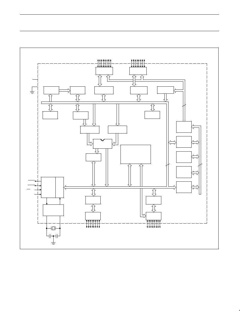
DESCRIPTION
Three different Single-Chip 8-Bit Microcontroller families are
presented in this datasheet:
∑
8XC54/8XC58
∑
80C51FA/8XC51FA/8XC51FB/8XC51FC
∑
80C51RA+/8XC51RA+/8XC51RB+/8XC51RC+/8XC51RD+
For applications requiring 4K ROM/EPROM, see the 8XC51/80C31
8-bit CMOS (low voltage, low power, and high speed)
microcontroller families datasheet.
All the families are Single-Chip 8-Bit Microcontrollers manufactured
in advanced CMOS process and are derivatives of the 80C51
microcontroller family. All the devices have the same instruction set
as the 80C51.
These devices provide architectural enhancements that make them
applicable in a variety of applications for general control systems.
ROM/EPROM
Memory Size
(X by 8)
RAM Size
(X by 8)
Programmable
Timer Counter
(PCA)
Hardware
Watch Dog
Timer
80C31/8XC51
0K/4K
128
No
No
8XC54/58
0K/8K/16K/32K
256
No
No
80C51FA/8XC51FA/FB/FC
0K/8K/16K/32K
256
Yes
No
80C51RA+/8XC51RA+/RB+/RC+
0K/8K/16K/32K
512
Yes
Yes
8XC51RD+
64K
1024
Yes
Yes
The ROMless devices, 80C51FA, and 80C51RA+ can address up to
64K of external memory. All the devices have four 8-bit I/O ports,
three 16-bit timer/event counters, a multi-source, four-priority-level,
nested interrupt structure, an enhanced UART and on-chip oscillator
and timing circuits. For systems that require extra memory capability
up to 64k bytes, each can be expanded using standard
TTL-compatible memories and logic.
Its added features make it an even more powerful microcontroller for
applications that require pulse width modulation, high-speed I/O and
up/down counting capabilities such as motor control. It also has a
more versatile serial channel that facilitates multiprocessor
communications.
FEATURES
∑
80C51 Central Processing Unit
∑
Speed up to 33 MHz
∑
Full static operation
∑
Operating voltage range:
2.7 V to 5.5 V @ 16 MHz
∑
Security bits:
≠ ROM ≠ 2 bits
≠ OTP≠EPROM ≠ 3 bits
∑
Encryption array ≠ 64 bytes
∑
RAM expandable to 64K bytes
∑
4 level priority interrupt
∑
6 or7 interrupt sources, depending on device
∑
Four 8-bit I/O ports
∑
Full-duplex enhanced UART
≠ Framing error detection
≠ Automatic address recognition
∑
Power control modes
≠ Clock can be stopped and resumed
≠ Idle mode
≠ Power down mode
∑
Programmable clock out
∑
Second DPTR register
∑
Asynchronous port reset
∑
Low EMI (inhibit ALE)
Philips Semiconductors
Product specification
8XC54/58
8XC51FA/FB/FC/80C51FA
8XC51RA+/RB+/RC+/RD+/80C51RA+
80C51 8-bit microcontroller family
8K≠64K/256≠1K OTP/ROM/ROMless, low voltage (2.7V≠5.5V),
low power, high speed (33 MHz)
2000 Aug 07
5
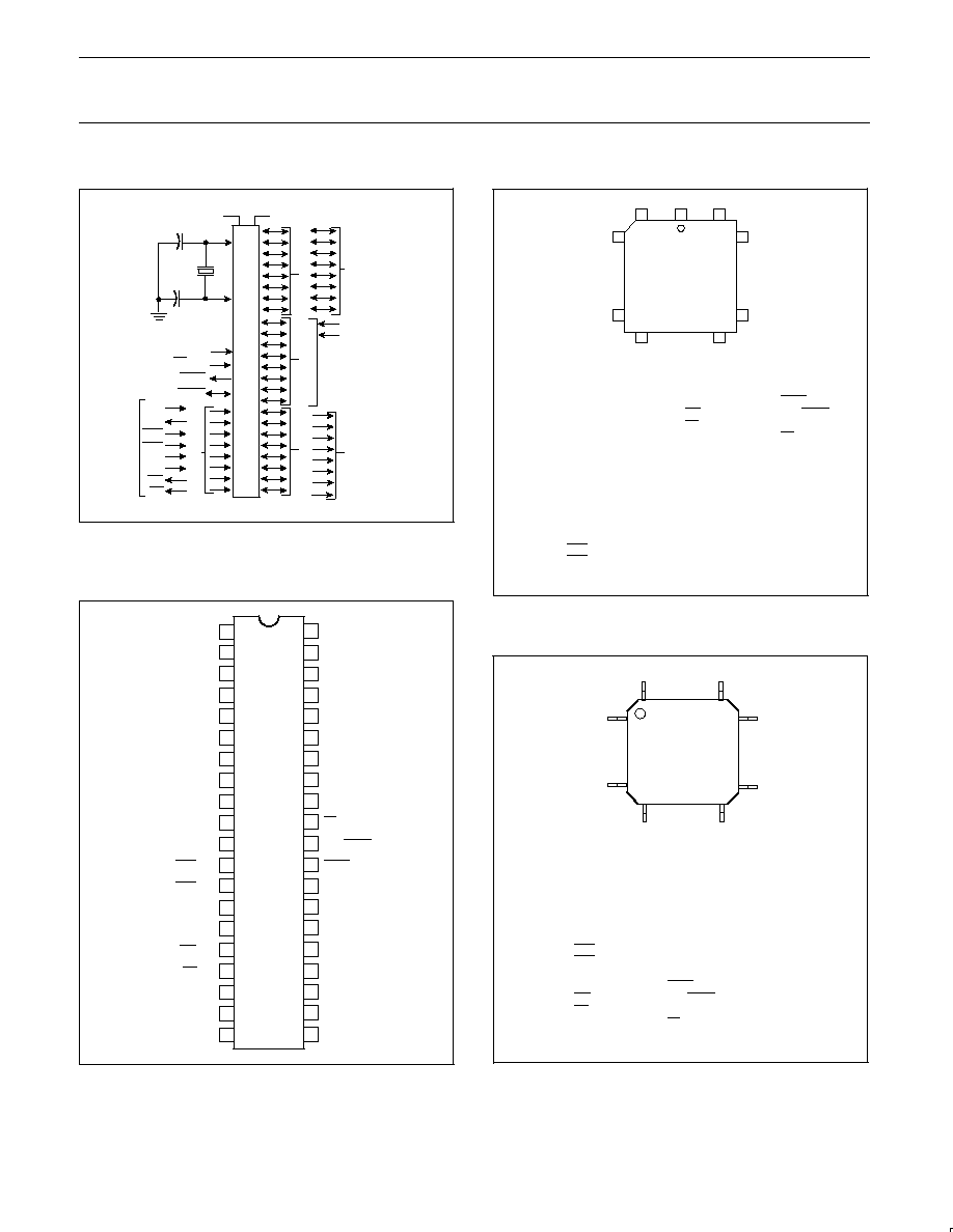
PIN DESCRIPTIONS
PIN NUMBER
MNEMONIC
DIP
LCC
QFP
TYPE
NAME AND FUNCTION
V
SS
20
22
16
I
Ground: 0 V reference.
V
CC
40
44
38
I
Power Supply: This is the power supply voltage for normal, idle, and power-down operation.
P0.0≠0.7
39≠32
43≠36
37≠30
I/O
Port 0: Port 0 is an open-drain, bidirectional I/O port. Port 0 pins that have 1s written to
them float and can be used as high-impedance inputs. Port 0 is also the multiplexed
low-order address and data bus during accesses to external program and data memory. In
this application, it uses strong internal pull-ups when emitting 1s. Port 0 also outputs the
code bytes during program verification and received code bytes during EPROM
programming. External pull-ups are required during program verification.
P1.0≠P1.7
1≠8
2≠9
40≠44,
1≠3
I/O
Port 1: Port 1 is an 8-bit bidirectional I/O port with internal pull-ups. Port 1 pins that have 1s
written to them are pulled high by the internal pull-ups and can be used as inputs. As inputs,
port 1 pins that are externally pulled low will source current because of the internal pull-ups.
(See DC Electrical Characteristics: I
IL
). Port 1 also receives the low-order address byte
during program memory verification.
Alternate functions for 8XC51FX and 8XC51RX+ Port 1 include:
1
2
40
I/O
T2 (P1.0): Timer/Counter 2 external count input/Clockout (see Programmable Clock-Out)
2
3
41
I
T2EX (P1.1): Timer/Counter 2 Reload/Capture/Direction Control
3
4
42
I
ECI (P1.2): External Clock Input to the PCA
4
5
43
I/O
CEX0 (P1.3): Capture/Compare External I/O for PCA module 0
5
6
44
I/O
CEX1 (P1.4): Capture/Compare External I/O for PCA module 1
6
7
1
I/O
CEX2 (P1.5): Capture/Compare External I/O for PCA module 2
7
8
2
I/O
CEX3 (P1.6): Capture/Compare External I/O for PCA module 3
8
9
3
I/O
CEX4 (P1.7): Capture/Compare External I/O for PCA module 4
P2.0≠P2.7
21≠28
24≠31
18≠25
I/O
Port 2: Port 2 is an 8-bit bidirectional I/O port with internal pull-ups. Port 2 pins that have 1s
written to them are pulled high by the internal pull-ups and can be used as inputs. As inputs,
port 2 pins that are externally being pulled low will source current because of the internal
pull-ups. (See DC Electrical Characteristics: I
IL
). Port 2 emits the high-order address byte
during fetches from external program memory and during accesses to external data memory
that use 16-bit addresses (MOVX @DPTR). In this application, it uses strong internal
pull-ups when emitting 1s. During accesses to external data memory that use 8-bit addresses
(MOV @Ri), port 2 emits the contents of the P2 special function register. Some Port 2 pins
receive the high order address bits during EPROM programming and verification.
P3.0≠P3.7
10≠17
11,
13≠19
5,
7≠13
I/O
Port 3: Port 3 is an 8-bit bidirectional I/O port with internal pull-ups. Port 3 pins that have 1s
written to them are pulled high by the internal pull-ups and can be used as inputs. As inputs,
port 3 pins that are externally being pulled low will source current because of the pull-ups.
(See DC Electrical Characteristics: I
IL
). Port 3 also serves the special features of the 80C51
family, as listed below:
10
11
5
I
RxD (P3.0): Serial input port
11
13
7
O
TxD (P3.1): Serial output port
12
14
8
I
INT0 (P3.2): External interrupt
13
15
9
I
INT1 (P3.3): External interrupt
14
16
10
I
T0 (P3.4): Timer 0 external input
15
17
11
I
T1 (P3.5): Timer 1 external input
16
18
12
O
WR (P3.6): External data memory write strobe
17
19
13
O
RD (P3.7): External data memory read strobe
RST
9
10
4
I
Reset: A high on this pin for two machine cycles while the oscillator is running, resets the
device. An internal diffused resistor to V
SS
permits a power-on reset using only an external
capacitor to V
CC
.
ALE/PROG
30
33
27
O
Address Latch Enable/Program Pulse: Output pulse for latching the low byte of the
address during an access to external memory. In normal operation, ALE is emitted at a
constant rate of 1/6 the oscillator frequency, and can be used for external timing or clocking.
Note that one ALE pulse is skipped during each access to external data memory. This pin is
also the program pulse input (PROG) during EPROM programming. ALE can be disabled by
setting SFR auxiliary.0. With this bit set, ALE will be active only during a MOVX instruction.