 | –≠–ª–µ–∫—Ç—Ä–æ–Ω–Ω—ã–π –∫–æ–º–ø–æ–Ω–µ–Ω—Ç: 83C748 | –°–∫–∞—á–∞—Ç—å:  PDF PDF  ZIP ZIP |

Philips
Semiconductors
83C748/87C748
80C51 8-bit microcontroller family
2K/64 OTP/ROM, low pin count
Preliminary specification
Supersedes data of 1998 Apr 23
IC20 Data Handbook
1999 Apr 15
INTEGRATED CIRCUITS
Philips Semiconductors
Preliminary specification
83C748/87C748
80C51 8-bit microcontroller family
2K/64 OTP/ROM, low pin count
2
1999 Apr 15
DESCRIPTION
The Philips 83C748/87C748 offers the advantages of the 80C51
architecture in a small package and at low cost.
The 8XC748 Microcontroller is fabricated with Philips high-density
CMOS technology. Philips epitaxial substrate minimizes CMOS
latch-up sensitivity.
The 8XC748 contains a 2k
◊
8 ROM (83C748) EPROM (87C748), a
64
◊
8 RAM, 19 I/O lines, a 16-bit auto-reload counter/timer, a
four-source, fixed-priority level interrupt structure, and an on-chip
oscillator.
FEATURES
∑
80C51 based architecture
∑
Small package sizes
≠ 24-pin DIP (300 mil "skinny DIP")
≠ 24-pin Shrink Small Outline Package (SSOP)
≠ 28-pin PLCC
∑
87C748 available in erasable quartz lid or one-time programmable
plastic packages
∑
Wide oscillator frequency range: ≠3.5 to 16MHz
∑
Low power consumption:
≠ Normal operation: less than 11mA @ 5V, 12MHz
≠ Idle mode
≠ Power-down mode
∑
2k
◊
8 ROM (83C748)
2k
◊
8 EPROM (87C748)
∑
64
◊
8 RAM
∑
16-bit auto reloadable counter/timer
∑
10-bit fixed-rate timer
∑
Boolean processor
∑
CMOS and TTL compatible
∑
Well suited for logic replacement, consumer and industrial
applications
∑
LED drive outputs
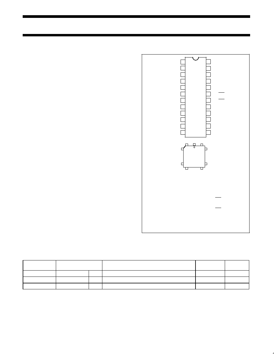
PIN CONFIGURATIONS
1
2
3
4
5
6
7
8
9
10
11
12
13
14
15
16
17
18
19
20
21
22
23
24
P3.4/A4
P3.3/A3
P3.2/A2/A10
P3.1/A1/A9
P3.0/A0/A8
P0.2/VPP
RST
X2
X1
V
SS
P0.0/ASEL
P1.0/D0
P1.1/D1
P1.2/D2
P1.3/D3
P1.4/D4
P1.5/INT0/D5
P1.6/INT1/D6
P1.7/T0/D7
P3.7/A7
P3.6/A6
P3.5/A5
V
CC
PLASTIC
DUAL
IN-LINE
AND
SHRINK
SMALL
OUTLINE
PACKAGE
PLASTIC
LEADED
CHIP
CARRIER
4
1
26
5
11
25
19
12
18
P0.1/OE≠PGM
Pin
Function
1
P3.4/A4
2
P3.3/A3
3
P3.2/A2/A10
4
P3.1/A1/A9
5
NC*
6
P3.0/A0/A8
7
P0.2/V
PP
8
P0.1/OE-PGM
9
P0.0/ASEL
10
NC*
11
RST
12
X2
13
X1
14
V
SS
Pin
Function
15
P1.0/D0
16
P1.1/D1
17
P1.2/D2
18
P1.3/D3
19
P1.4/D4
20
P1.5/INT0/D5
21
NC*
22
NC*
23
P1.6/INT1/D6
24
P1.7/T0/D7
25
P3.7/A7
26
P3.6/A6
27
P3.5/A5
28
V
CC
SU00295A
* NO INTERNAL CONNECTION
ORDERING INFORMATION
ROM
EPROM
1
TEMPERATURE RANGE
∞
C
AND PACKAGE
FREQUENCY
MHz
DRAWING
NUMBER
P83C748EBP N
P87C748EBP N
OTP
0 to +70, Plastic Dual In-line Package
3.5 to 16
SOT222-1
P83C748EBA A
P87C748EBA A
OTP
0 to +70, Plastic Leaded Chip Carrier
3.5 to 16
SOT261-3
P83C748EBD DB
P87C748EBD DB
OTP
0 to +70, Shrink Small Outline Package
3.5 to 16
SOT340-1
NOTE:
1. OTP = One Time Programmable EPROM.
Philips Semiconductors
Preliminary specification
83C748/87C748
80C51 8-bit microcontroller family
2K/64 OTP/ROM, low pin count
1999 Apr 15
3
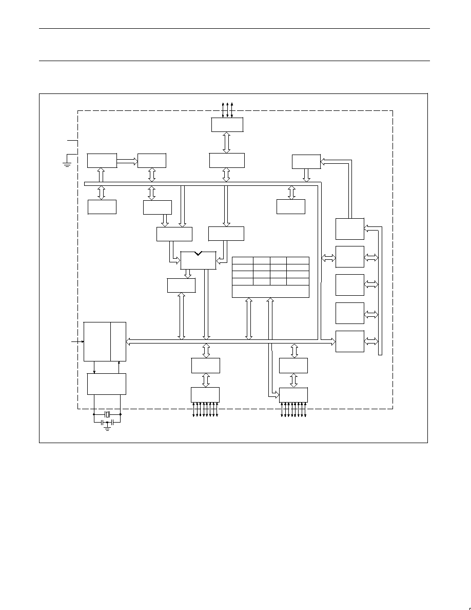
BLOCK DIAGRAM
RST
X1
X2
VCC
VSS
RAM
ROM/
EPROM
ACC
TMP2
TMP1
ALU
INSTRUCTION
REGISTER
PD
OSCILLATOR
PSW
BUFFER
DPTR
PCON
TCON
IE
TH0
TL0
RTH
RTL
INTERRUPT AND
TIMER BLOCKS
P1.0≠P1.7
P3.0≠P3.7
P0.0≠P0.2
PORT 0
DRIVERS
RAM ADDR
REGISTER
PORT 0
LATCH
STACK
POINTER
PROGRAM
ADDRESS
REGISTER
PC
INCRE-
MENTER
PROGRAM
COUNTER
PORT 3
DRIVERS
PORT 1
DRIVERS
PORT 3
LATCH
PORT 1
LATCH
TIMING
AND
CONTROL
B
REGISTER
SU00296
Philips Semiconductors
Preliminary specification
83C748/87C748
80C51 8-bit microcontroller family
2K/64 OTP/ROM, low pin count
1999 Apr 15
4
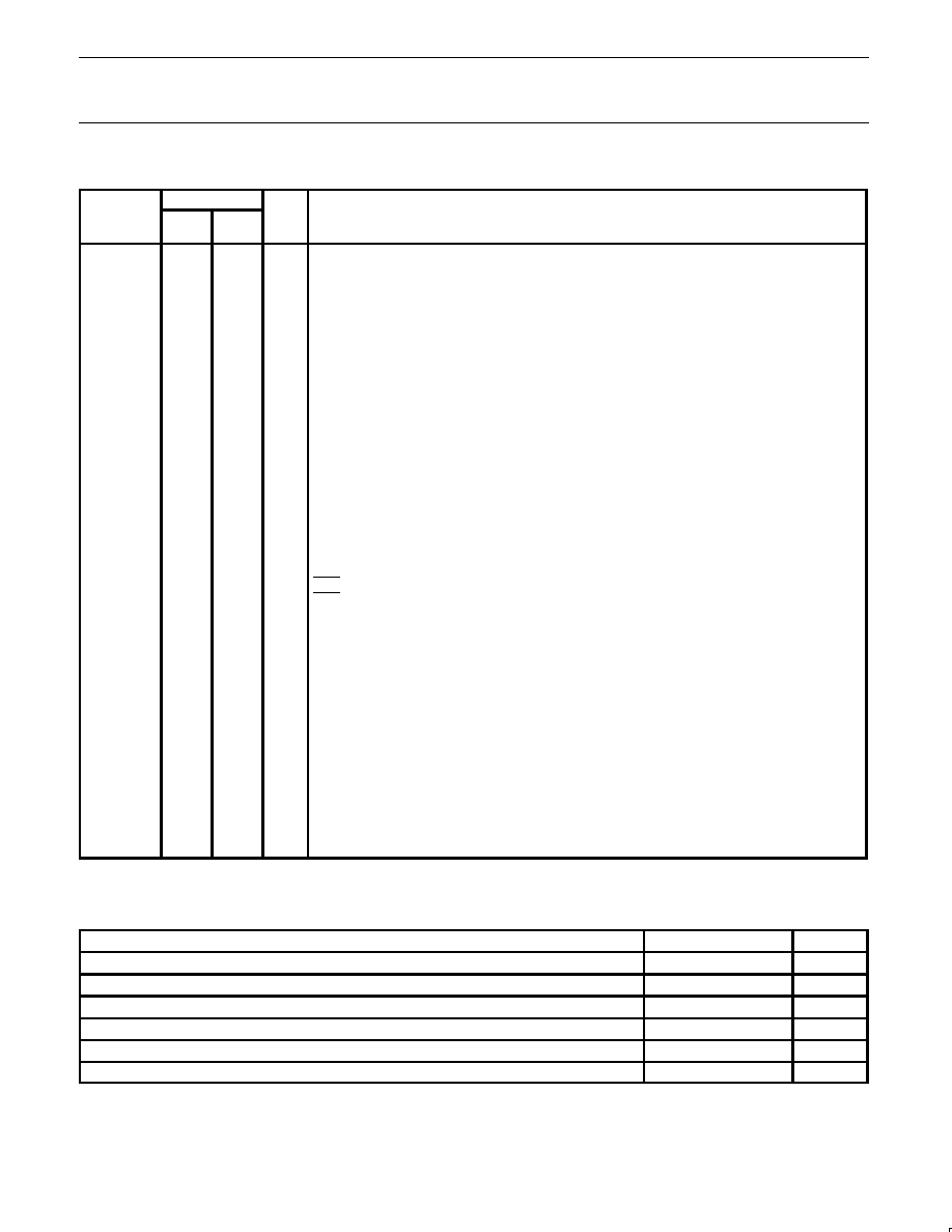
PIN DESCRIPTIONS
PIN NO.
MNEMONIC
DIP/
SSOP
LCC
TYPE
NAME AND FUNCTION
V
SS
12
14
I
Circuit Ground Potential
V
CC
24
28
I
Supply voltage during normal, idle, and power-down operation.
P0.0≠P0.2
8≠6
9≠7
I/O
Port 0: Port 0 is a 3-bit open-drain, bidirectional port. Port 0 pins that have 1s written to them float,
and in that state can be used as high-impedance inputs. These pins are driven low if the port register
bit is written with a 0. The state of the pin can always be read from the port register by the program.
P0.0 and P0.1 are open drain bidirectional I/O pins. While these differ from "standard TTL"
characteristics, they are close enough for the pins to still be used as general-purpose I/O. Port 0
also provides alternate functions for programming the EPROM memory as follows:
6
7
N/A
V
PP
(P0.2) ≠ Programming voltage input. (See Note 1).
7
8
I
OE/PGM (P0.1) ≠ Input which specifies verify mode (output enable) or the program mode.
OE/PGM = 1 output enabled (verify mode).
OE/PGM = 0 program mode.
8
9
I
ASEL (P0.0) ≠ Input which indicates which bits of the EPROM address are applied to port 3.
ASEL = 0 low address byte available on port 3.
ASEL = 1 high address byte available on port 3 (only the three least significant bits are used).
P1.0≠P1.7
13≠20
15≠20,
23, 24
I/O
Port 1: Port 1 is an 8-bit bidirectional I/O port with internal pull-ups. Port 1 pins that have 1s written
to them are pulled high by the internal pull-ups and can be used as inputs. As inputs, port 1 pins
that are externally pulled low will source current because of the internal pull-ups. (See DC Electrical
Characteristics: I
IL
). Port 1 serves to output the addressed EPROM contents in the verify mode and
accepts as inputs the value to program into the selected address during the program mode. Port 1
also serves the special function features of the 80C51 family as listed below:
18
20
I
INT0 (P1.5): External interrupt.
19
23
I
INT1 (P1.6): External interrupt.
20
24
I
T0 (P1.7): Timer 0 external input.
P3.0≠P3.7
5≠1,
23≠21
6, 4≠1,
27≠25
I/O
Port 3: Port 3 is an 8-bit bidirectional I/O port with internal pull-ups. Port 3 pins that have 1s written
to them are pulled high by the internal pull-ups and can be used as inputs. As inputs, port 3 pins
that are externally being pulled low will source current because of the pull-ups. (See DC Electrical
Characteristics: I
IL
). Port 3 also functions as the address input for the EPROM memory location to be
programmed (or verified). The 11-bit address is multiplexed into this port as specified by P0.0/ASEL.
RST
9
11
I
Reset: A high on this pin for two machine cycles while the oscillator is running, resets the device.
An internal diffused resistor to V
SS
permits a power-on RESET using only an external capacitor to
V
CC
. After the device is reset, a 10-bit serial sequence, sent LSB first, applied to RESET, places
the device in the programming state allowing programming address, data and V
PP
to be applied for
programming or verification purposes. The RESET serial sequence must be synchronized with the
X1 input.
X1
11
13
I
Crystal 1: Input to the inverting oscillator amplifier and input to the internal clock generator circuits.
X1 also serves as the clock to strobe in a serial bit stream into RESET to place the device in the
programming state.
X2
10
12
O
Crystal 2: Output from the inverting oscillator amplifier.
NOTE:
1. When P0.2 is at or close to 0 volts, it may affect the internal ROM operation. It is recommended that P0.2 be tied to V
CC
via a small pull-up
(e.g. 2k
W
).
ABSOLUTE MAXIMUM RATINGS
1, 2
PARAMETER
RATING
UNIT
Storage temperature range
≠65 to +150
∞
C
Voltage from V
CC
to V
SS
≠0.5 to +6.5
V
Voltage from any pin to V
SS
(except V
PP
)
≠0.5 to V
CC
+ 0.5
V
Power dissipation
1.0
W
Voltage on V
PP
pin to V
SS
0 to +13.0
V
Maximum I
OL
per I/O pin
10
mA
NOTES:
1. Stresses above those listed under Absolute Maximum Ratings may cause permanent damage to the device. This is a stress rating only and
functional operation of the device at these or any conditions other than those described in the AC and DC Electrical Characteristics section
of this specification is not implied.
2. This product includes circuitry specifically designed for the protection of its internal devices from the damaging effects of excessive static
charge. Nonetheless, it is suggested that conventional precautions be taken to avoid applying greater than the rated maxima.
Philips Semiconductors
Preliminary specification
83C748/87C748
80C51 8-bit microcontroller family
2K/64 OTP/ROM, low pin count
1999 Apr 15
5
DC ELECTRICAL CHARACTERISTICS
T
amb
= 0
∞
C to +70
∞
C, V
CC
= 5V
±
10%, V
SS
= 0V
1
SYMBOL
PARAMETER
TEST CONDITIONS
LIMITS
UNIT
SYMBOL
PARAMETER
TEST CONDITIONS
MIN
MAX
UNIT
V
IL
Input low voltage
≠0.5
0.2V
DD
≠0.1
V
V
IH
Input high voltage, except X1, RST
0.2V
CC
+0.9
V
CC
+0.5
V
V
IH1
Input high voltage, X1, RST
0.7V
CC
V
CC
+0.5
V
P0.2
V
IL1
Input low voltage
≠0.5
0.3V
CC
V
V
IH2
Input high voltage
0.7V
CC
V
CC
+0.5
V
V
OL
Output low voltage, ports 1 and 3
I
OL
= 1.6mA
2
0.45
V
V
OL1
Output low voltage, port 0.2
I
OL
= 3.2mA
2
0.45
V
V
OH
Output high voltage, ports 1 and 3
I
OH
= ≠60
µ
A
2.4
V
I
OH
= ≠25
µ
A
0.75V
CC
V
I
OH
= ≠10
µ
A
0.9V
CC
V
Port 0.0 and 0.1 ≠ Drivers
V
OL2
Output low voltage
I
OL
= 3mA
0.4
V
Driver, receiver combined:
(over V
CC
range)
C
Capacitance
10
pF
I
IL
Logical 0 input current, ports 1 and 3
V
IN
= 0.45V
≠50
µ
A
I
TL
Logical 1 to 0 transition current, ports 1 and 3
3
V
IN
= 2V (0 to 70
∞
C)
≠650
µ
A
I
LI
Input leakage current, port 0
0.45 < V
IN
< V
CC
±
10
µ
A
R
RST
Internal pull-down resistor
25
175
k
C
IO
Pin capacitance
Test freq = 1MHz,
T
amb
= 25
∞
C
10
pF
I
PD
Power-down current
4
V
CC
= 2 to V
CC
max
50
µ
A
V
PP
V
PP
program voltage (for 87C748 only)
V
SS
= 0V
V
CC
= 5V
±
10%
T
amb
= 21
∞
C to 27
∞
C
12.5
13.0
V
I
PP
Program current (for 87C748 only)
V
PP
= 13.0V
50
mA
I
CC
Supply current (see Figure 2)
NOTES:
1. Parameters are valid over operating temperature range unless otherwise specified. All voltages are with respect to V
SS
unless otherwise
noted.
2. Under steady state (non-transient) conditions, I
OL
must be externally limited as follows:
Maximum I
OL
per port pin:
10mA
Maximum I
OL
per 8-bit port:
26mA
Maximum total I
OL
for all outputs:
67mA
If I
OL
exceeds the test condition, V
OL
may exceed the related specification. Pins are not guaranteed to sink current greater than the listed
test conditions.
3. Pins of ports 1 and 3 source a transition current when they are being externally driven from 1 to 0. The transition current reaches its
maximum value when V
IN
is approximately 2V.
4. Power-down I
CC
is measured with all output pins disconnected; port 0 = V
CC
; X2, X1 n.c.; RST = V
SS
.
5. Active I
CC
is measured with all output pins disconnected; X1 driven with t
CLCH
, t
CHCL
= 5ns, V
IL
= V
SS
+ 0.5V, V
IH
= V
CC
≠ 0.5V; X2 n.c.;
RST = port 0 = V
CC
. I
CC
will be slightly higher if a crystal oscillator is used.
6. Idle I
CC
is measured with all output pins disconnected; X1 driven with t
CLCH
, t
CHCL
= 5ns, V
IL
= V
SS
+ 0.5V, V
IH
= V
CC
≠ 0.5V; X2 n.c.;
port 0 = V
CC
; RST = V
SS
.
Philips Semiconductors
Preliminary specification
83C748/87C748
80C51 8-bit microcontroller family
2K/64 OTP/ROM, low pin count
1999 Apr 15
6
AC ELECTRICAL CHARACTERISTICS
T
amb
= 0
∞
C to +70
∞
C, V
CC
= 5V
±
10%, V
SS
= 0V
1, 2
16MHz CLOCK
VARIABLE CLOCK
SYMBOL
PARAMETER
MIN
MAX
MIN
MAX
UNIT
1/t
CLCL
Oscillator frequency:
3.5
12
MHz
3.5
16
MHz
External Clock (Figure 1)
t
CHCX
High time
20
20
ns
t
CLCX
Low time
20
20
ns
t
CLCH
Rise time
20
20
ns
t
CHCL
Fall time
20
20
ns
NOTES:
1. Parameters are valid over operating temperature range unless otherwise specified. All voltages are with respect to V
SS
unless otherwise
noted.
2. Load capacitance for ports = 80pF.
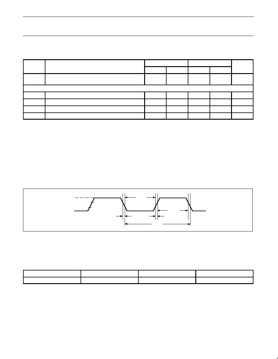
EXPLANATION OF THE AC SYMBOLS
Each timing symbol has five characters. The first character is always
`t' (= time). The other characters, depending on their positions,
indicate the name of a signal or the logical status of that signal. The
designations are:
C ≠ Clock
D ≠ Input data
H ≠ Logic level high
L ≠ Logic level low
Q ≠ Output data
T ≠ Time
V ≠ Valid
X ≠ No longer a valid logic level
Z ≠ Float
t
CHCL
t
CLCL
t
CLCH
t
CHCX
V
CC
≠0.5
0.45V
0.2 V
CC
+ 0.9
0.2 V
CC
≠ 0.1
t
CLCX
SU00297
Figure 1. External Clock Drive
ROM CODE SUBMISSION
When submitting ROM code for the 83C748, the following must be specified:
1. 2k byte user ROM data
ADDRESS
CONTENT
BIT(S)
COMMENT
0000H to 07FFH
DATA
7:0
User ROM Data
Philips Semiconductors
Preliminary specification
83C748/87C748
80C51 8-bit microcontroller family
2K/64 OTP/ROM, low pin count
1999 Apr 15
7
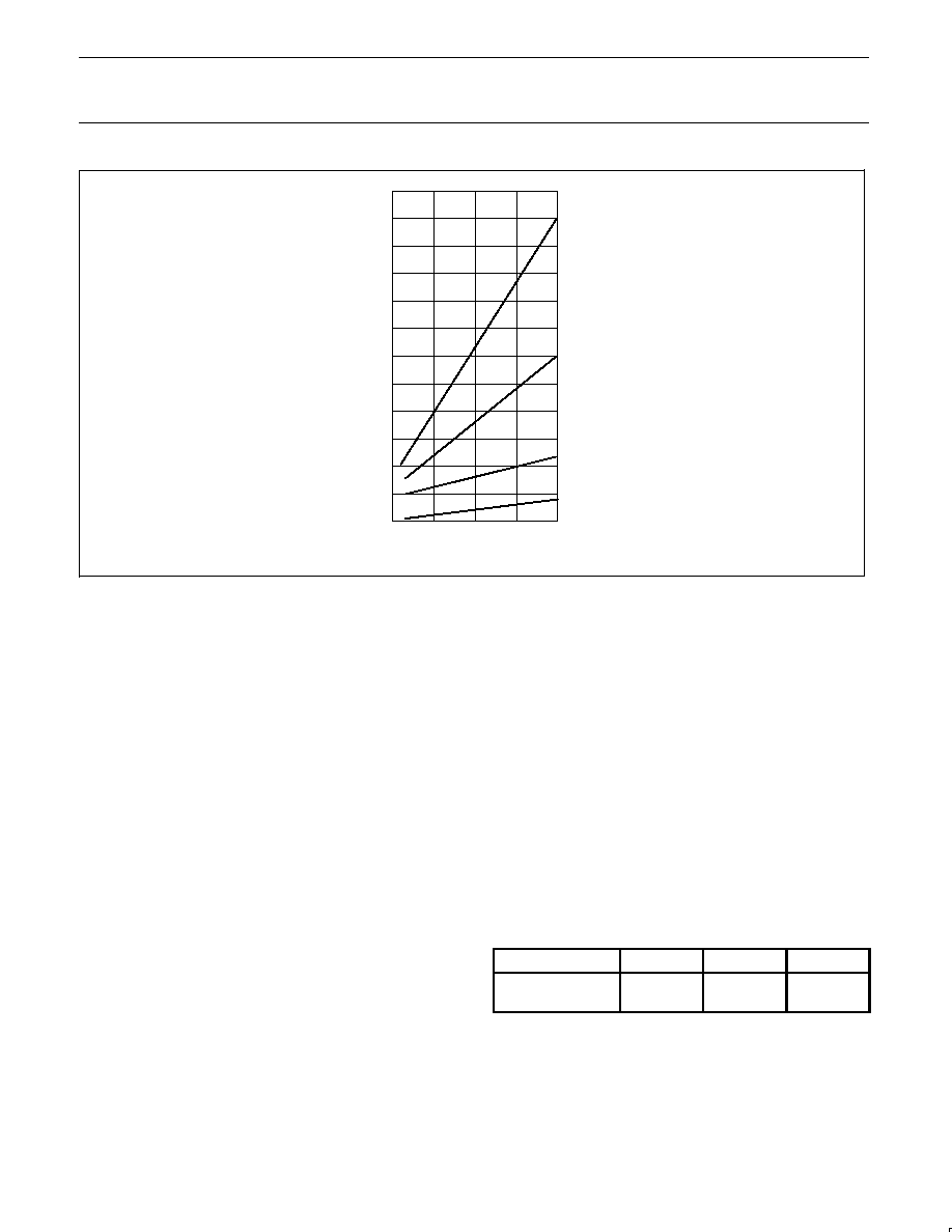
4MHz
8MHz
12MHz
16MHz
FREQ
MAX ACTIVE ICC
5
TYP ACTIVE ICC
5
MAX IDLE ICC
6
TYP IDLE ICC
6
ICC (mA)
2
4
6
8
10
12
14
16
18
20
22
SU00298
Figure 2. I
CC
vs. FREQ
Maximum I
CC
values taken at V
CC
max and worst case temperature.
Typical I
CC
values taken at V
CC
= 5.0V and 25
∞
C.
Notes 5 and 6 refer to DC Electrical Characteristics.
OSCILLATOR CHARACTERISTICS
X1 and X2 are the input and output, respectively, of an inverting
amplifier which can be configured for use as an on-chip oscillator.
To drive the device from an external clock source, X1 should be
driven while X2 is left unconnected. There are no requirements on
the duty cycle of the external clock signal, because the input to the
internal clock circuitry is through a divide-by-two flip-flop. However,
minimum and maximum high and low times specified in the data
sheet must be observed.
RESET
A reset is accomplished by holding the RST pin high for at least two
machine cycles (24 oscillator periods), while the oscillator is running.
To insure a good power-up reset, the RST pin must be high long
enough to allow the oscillator time to start up (normally a few
milliseconds) plus two machine cycles. At power-up, the voltage on
V
CC
and RST must come up at the same time for a proper start-up.
IDLE MODE
In idle mode, the CPU puts itself to sleep while all of the on-chip
peripherals stay active. The instruction to invoke the idle mode is the
last instruction executed in the normal operating mode before the
idle mode is activated. The CPU contents, the on-chip RAM, and all
of the special function registers remain intact during this mode. The
idle mode can be terminated either by any enabled interrupt (at
which time the process is picked up at the interrupt service routine
and continued), or by a hardware reset which starts the processor in
the same manner as a power-on reset.
POWER-DOWN MODE
In the power-down mode, the oscillator is stopped and the
instruction to invoke power-down is the last instruction executed.
Only the contents of the on-chip RAM are preserved. A hardware
reset is the only way to terminate the power-down mode. the control
bits for the reduced power modes are in the special function register
PCON.
Table 1.
External Pin Status During Idle and
Power-Down Modes
MODE
Port 0
Port 1
Port 2
Idle
Data
Data
Data
Power-down
Data
Data
Data

Philips Semiconductors
Preliminary specification
83C748/87C748
80C51 8-bit microcontroller family
2K/64 OTP/ROM, low pin count
1999 Apr 15
8
DIFFERENCES BETWEEN THE 8XC748 AND THE
80C51
Memory Organization
The central processing unit (CPU) manipulates operands in two
address spaces as shown in Figure 3. The part's internal memory
space consists of 2k bytes of program memory, and 64 bytes of data
RAM overlapped with the 128-byte special function register area.
The differences from the 80C51 are in RAM size (64 bytes vs. 128
bytes), in external RAM access (not available on the 83C748), in
internal ROM size (2k bytes vs. 4k bytes), and in external program
memory expansion (not available on the 83C748). The 128-byte
special function register (SFR) space is accessed as on the 80C51
with some of the registers having been changed to reflect changes
in the 83C748 peripheral functions. The stack may be located
anywhere in internal RAM by loading the 8-bit stack pointer (SP). It
should be noted that stack depth is limited to 64 bytes, the amount
of available RAM. A reset loads the stack pointer with 07 (which is
pre-incremented on a PUSH instruction).
Program Memory
On the 8XC748, program memory is 2048 bytes long and is not
externally expandable, so the 80C51 instructions MOVX, LJMP, and
LCALL are not implemented. The only fixed locations in program
memory are the addresses at which execution is taken up in
response to reset and interrupts, which are as follows:
Program Memory
Event
Address
Reset
000
External INT0
003
Counter/timer 0
00B
External INT1
013
Timer I
01B
Counter/Timer Subsystem
The 8XC748 has one counter/timer called timer/counter 0. Its
operation is similar to mode 2 operation on the 80C51, but is
extended to 16 bits with 16 bits of autoload. The controls for this
counter are centralized in a single register called TCON.
Timer I is available for use as a fixed 10-bit time-base, or as a
watchdog.
Counter Timer ≠ Special Function Register
The counter/timer has only one mode of operation, so the TMOD
SFR is not used. There is also only one counter/timer, so there is no
need for the TL1 and TH1 SFRs found on the 80C51. These have
been replaced on the 8XC748 by RTL and RTH, the counter/timer
reload registers. Table 2 shows the special function registers, their
locations, and reset values.
Interrupt Subsystem ≠ Fixed Priority
The IP register and the 2-level interrupt system of the 80C51 are
eliminated. Simultaneous interrupt conditions are resolved by a
single-level, fixed priority as follows:
Highest priority:
Pin INT0
Counter/timer flag 0
Pin INT1
Lowest priority:
Timer I
Special Function Register ≠ Interrupt Subsystem
Because the interrupt structure is single level on the 83C748, there
is no need for the IP SFR, so it is not used.
Special Function Register ≠
Serial Communications
The 8XC748 contains many of the special function registers (SFR)
that are found on the 80C51. Due to the different peripheral features
on the 8XC748, there are several additional SFRs. Since the UART
found on 80C51 has been removed, the UART SFRs SCON and
SBUF have also been removed.
I/O Port Latches (P0, P1, P3)
The port latches function the same as those on the 80C51. Since
there is no port 2 on the 83C748, the P2 latch is not used. Port 0 on
the 83C748 has only 3 bits, so only 3 bits of the P0 SFR have a
useful function.
Data Pointer (DPTR)
The data pointer (DPTR) consists of a high byte (DPH) and a low
byte (DPL). In the 80C51 this register allows the access of external
data memory using the MOVX instruction. Since the 83C748 does
not support MOVX or external memory accesses, this register is
generally used as a 16-bit offset pointer of the accumulator in a
MOVC instruction. DPTR may also be manipulated as two
independent 8-bit registers.
Special
Function
Registers
Internal Data
RAM
(FFH) 255
(80H) 128
(3FH) 63
(00H) 0
SU00299
Figure 3. Memory Map
Philips Semiconductors
Preliminary specification
83C748/87C748
80C51 8-bit microcontroller family
2K/64 OTP/ROM, low pin count
1999 Apr 15
9
Table 2.
8XC748 Special Function Registers
SYMBOL
DESCRIPTION
DIRECT
ADDRESS
BIT ADDRESS, SYMBOL, OR ALTERNATIVE PORT FUNCTION
MSB
LSB
RESET
VALUE
ACC*
Accumulator
E0H
E7
E6
E5
E4
E3
E2
E1
E0
00H
B*
B register
F0H
F7
F6
F5
F4
F3
F2
F1
F0
00H
DPTR:
DPH
DPL
Data pointer
(2 bytes)
High byte
Low byte
83H
82H
00H
00H
AF
AE
AD
AC
AB
AA
A9
A8
IE*#
Interrupt enable
ABH
EA
≠
≠
≠
ETI
EX1
ET0
EX0
00H
82
81
80
P0*#
Port 0
80H
≠
≠
≠
≠
≠
≠
≠
≠
xxxxx111B
97
96
95
94
93
92
91
90
P1*
Port 1
90H
T0
INT1
INT0
≠
≠
≠
≠
≠
FFH
P3*
Port 3
B0H
B7
B6
B5
B4
B3
B2
B1
B0
FFH
PCON#
Power control
87H
≠
≠
≠
≠
≠
≠
PD
IDL
xxxxxx00B
D7
D6
D5
D4
D3
D2
D1
D0
PSW*
Program status word
D0H
CY
AC
F0
RS1
RS0
OV
≠
P
00H
SP
Stack pointer
81H
07H
8F
8E
8D
8C
8B
8A
89
88
TCON*#
Timer/counter control
88H
GATE
C/T
TF
TR
IE0
IT0
IE1
IT1
00H
TL#
Timer low byte
8AH
00H
TH#
Timer high byte
8CH
00H
DF
DE
DD
DC
DB
DA
D9
D8
TICON*#
Timer I control
D8H/RD
≠
≠
0
TIRUN
≠
≠
≠
≠
0000xx00B
WR
≠
≠
CLRTI
TIRUN
≠
≠
≠
≠
RTL#
Timer low reload
8BH
00H
RTH#
Timer high reload
8DH
00H
*
SFRs are bit addressable.
#
SFRs are modified from or added to the 80C51 SFRs.
I/O Port Structure
The 8XC748 has two 8-bit ports (ports 1 and 3) and one 3-bit port
(port 0). All three ports on the 8XC748 are bidirectional. Each
consists of a latch (special function register P0, P1, P3), an output
driver, and an input buffer. Three port 1 pins and two port 0 pins are
multifunctional. In addition to being port pins, these pins serve the
function of special features as follows:
Port Pin
Alternate Function
P1.5
INT0 (external interrupt 0 input)
P1.6
INT1 (external interrupt 1 input)
P1.7
T0 (timer 0 external input)
Ports 1 and 3 are identical in structure to the same ports on the
80C51. The structure of port 0 on the 8XC748 is similar to that of the
80C51 but does not include address/data input and output circuitry.
As on the 80C51, ports 1 and 3 are quasi-bidirectional while port 0 is
bidirectional with no internal pullups.
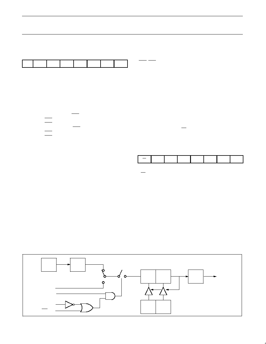
Timer/Counter
The 8XC748 has two timers: a 16-bit timer/counter and a 10-bit
fixed-rate timer. The 16-bit timer/counter's operation is similar to
mode 2 operation on the 80C51, but is extended to 16 bits. The
timer/counter is clocked by either 1/12 the oscillator frequency or by
transitions on the T0 pin. The C/T pin in special function register
TCON selects between these two modes. When the TCON TR bit is
set, the timer/counter is enabled. Register pair TH and TL are
incremented by the clock source. When the register pair overflows,
the register pair is reloaded with the values in registers RTH and
RTL. The value in the reload registers is left unchanged. See the
83C748 counter/timer block diagram in Figure 4. The TF bit in
special function register TCON is set on counter overflow and, if the
interrupt is enabled, will generate an interrupt.
Philips Semiconductors
Preliminary specification
83C748/87C748
80C51 8-bit microcontroller family
2K/64 OTP/ROM, low pin count
1999 Apr 15
10
TCON Register
MSB
LSB
GATE
C/T
TF
TR
IE0
IT0
IE1
IT1
GATE
1 ≠ Timer/counter is enabled only when INT0 pin is high,
and TR is 1.
0 ≠ Timer/counter is enabled when TR is 1.
C/T
1 ≠ Counter/timer operation from T0 pin.
0 ≠ Timer operation from internal clock.
TF
1 ≠ Set on overflow of TH.
0 ≠ Cleared when processor vectors to interrupt routine
and by reset.
TR
1 ≠ Timer/counter enabled.
0 ≠ Timer/counter disabled.
IE0
1 ≠ Edge detected in INT0.
IT0
1 ≠ INT0 is edge triggered.
0 ≠ INT0 is level sensitive.
IE1
1 ≠ Edge detected on INT1.
IT1
1 ≠ INT1 is edge triggered.
0 ≠ INT1 is level sensitive.
These flags are functionally identical to the corresponding 80C51
flags, except that there is only one timer on the 83C748 and the
flags are therefore combined into one register.
Note that the positions of the IE0/IT0 and IE1/IT1 bits are transposed
from the positions used in the standard 80C51 TCON register.
Timer I Implementation
Timer I is clocked once per machine cycle, which is the oscillator
frequency divided by 12. The timer operation is enabled by setting
the TIRUN bit (bit 4) in the I2CFG register. Writing a 0 into the
TIRUN bit will stop and clear the timer. The timer is 10 bits wide, and
when it reaches the terminal count of 1024, it carries out and sets
the Timer I interrupt flag. An interrupt will occur if the Timer I
interrupt is enabled by bit ETI (bit 4) of the Interrupt Enable (IE)
register, and global interrupts are enabled by bit EA (bit 7) of the
same IE register.
The vector address for the Timer I interrupt is 1Bhex, and the
interrupt service routine must start at this address. As with all 8051
family microcontrollers, only the Program Counter is pushed onto
the stack upon interrupt (other registers that are used both by the
interrupt service routine and elsewhere must be explicitly saved).
The Timer I interrupt flag is cleared by setting the CKRTI bit (bit 5 of
the I1CFG register. For more information, see application note
AN427.
Interrupts
The interrupt structure is a four-source, one-level interrupt system.
Interrupt sources common to the 80C51 are the external interrupts
(INT0, INT1) and the timer/counter interrupt (ET0). Timer I interrupt
(ETI) is the other interrupt source. The interrupt sources are listed
below in their order of polling sequence priority.
Upon interrupt or reset the program counter is loaded with specific
values for the appropriate interrupt service routine in program
memory. These values are:
Program Memory
Event
Address
Priority
Reset
000
Highest
INT0
003
Counter/Timer 0
00B
INT1
013
Timer I
01B
Lowest
The interrupt enable register (IE) is used to individually enable or
disable the four sources. Bit EA in the interrupt enable register can
be used to globally enable or disable all interrupt sources. The
interrupt enable register is described below. All other interrupt details
are based on the 80C51 interrupt architecture.
Interrupt Enable Register
EA
X
X
--
ETI
EX1
ET0
EX0
Symbol Position
Function
EA
IE.7
Disables all interrupts. If EA = 0, no interrupt
will be acknowledged. If EA = 1, each
interrupt source is individually enabled or
disabled by setting or clearing its enable bit
≠
IE.6
Reserved
≠
IE.5
Reserved
≠
IE.4
Reserved
ETI
IE.3
Enables or disables the Timer I overflow
interrupt. If ET1 = 0, the Timer I interrupt is
disabled.
EX1
IE.2
Enables or disables external interrupt 1.
If EX1 = 0, external interrupt 1 is disabled.
ET0
IE.1
Enables or disables the Timer 0 overflow
interrupt. If ET0 = 0, theTimer 0 interrupt is
disabled.
EX0
IE.0
Enables or disables external interrupt 0.
If EX0 = 0, external interrupt 0 is disabled.
OSC
˜
12
TL
TH
TF
RTL
RTH
T0 Pin
TR
Gate
INT0 Pin
Int.
C/T = 0
C/T = 1
Reload
SU00300
Figure 4. 83C748 Counter/Timer Block Diagram

Philips Semiconductors
Preliminary specification
83C748/87C748
80C51 8-bit microcontroller family
2K/64 OTP/ROM, low pin count
1999 Apr 15
11
87C748 PROGRAMMING CONSIDERATIONS
EPROM Characteristics
The 87C748 is programmed by using a modified Quick-Pulse
Programming algorithm similar to that used for devices such as the
87C451 and 87C51. It differs from these devices in that a serial data
stream is used to place the 87C748 in the programming mode.
Figure 5 shows a block diagram of the programming configuration
for the 87C748. Port pin P0.2 is used as the programming voltage
supply input (V
PP
signal). Port pin P0.1 is used as the program
(PGM/) signal. This pin is used for the 25 programming pulses.
Port 3 is used as the address input for the byte to be programmed
and accepts both the high and low components of the eleven bit
address. Multiplexing of these address components is performed
using the ASEL input. The user should drive the ASEL input high
and then drive port 3 with the high order bits of the address. ASEL
should remain high for at least 13 clock cycles. ASEL may then be
driven low which latches the high order bits of the address internally.
the high address should remain on port 3 for at least two clock
cycles after ASEL is driven low. Port 3 may then be driven with the
low byte of the address. The low address will be internally stable 13
clock cycles later. The address will remain stable provided that the
low byte placed on port 3 is held stable and ASEL is kept low. Note:
ASEL needs to be pulsed high only to change the high byte of the
address.
Port 1 is used as a bidirectional data bus during programming and
verify operations. During programming mode, it accepts the byte to
be programmed. During verify mode, it provides the contents of the
EPROM location specified by the address which has been supplied
to Port 3.
The XTAL1 pin is the oscillator input and receives the master system
clock. This clock should be between 1.2 and 6MHz.
The RESET pin is used to accept the serial data stream that places
the 87C748 into various programming modes. This pattern consists
of a 10-bit code with the LSB sent first. Each bit is synchronized to
the clock input, X1.
Programming Operation
Figures 6 and 7 show the timing diagrams for the program/verify
cycle. RESET should initially be held high for at least two machine
cycles. P0.1 (PGM/) and P0.2 (V
PP
) will be at V
OH
as a result of the
RESET operation. At this point, these pins function as normal
quasi-bidirectional I/O ports and the programming equipment may
pull these lines low. However, prior to sending the 10-bit code on the
RESET pin, the programming equipment should drive these pins
high (V
IH
). The RESET pin may now be used as the serial data input
for the data stream which places the 87C748 in the programming
mode. Data bits are sampled during the clock high time and thus
should only change during the time that the clock is low. Following
transmission of the last data bit, the RESET pin should be held low.
Next the address information for the location to be programmed is
placed on port 3 and ASEL is used to perform the address
multiplexing, as previously described. At this time, port 1 functions
as an output.
A high voltage V
PP
level is then applied to the V
PP
input (P0.2).
(This sets Port 1 as an input port). The data to be programmed into
the EPROM array is then placed on Port 1. This is followed by a
series of programming pulses applied to the PGM/ pin (P0.1). These
pulses are created by driving P0.1 low and then high. This pulse is
repeated until a total of 25 programming pulses have occurred. At
the conclusion of the last pulse, the PGM/ signal should remain high.
The V
PP
signal may now be driven to the V
OH
level, placing the
87C748 in the verify mode. (Port 1 is now used as an output port).
After four machine cycles (48 clock periods), the contents of the
addressed location in the EPROM array will appear on Port 1.
The next programming cycle may now be initiated by placing the
address information at the inputs of the multiplexed buffers, driving
the V
PP
pin to the V
PP
voltage level, providing the byte to be
programmed to Port1 and issuing the 26 programming pulses on the
PGM/ pin, bringing V
PP
back down to the V
C
level and verifying the
byte.
Programming Modes
The 87C748 has four programming features incorporated within its
EPROM array. These include the USER EPROM for storage of the
application's code, a 16-byte encryption key array and two security
bits. Programming and verification of these four elements are
selected by a combination of the serial data stream applied to the
RESET pin and the voltage levels applied to port pins P0.1 and
P0.2. The various combinations are shown in Table 3.
Table 3. Implementing Program/Verify Modes
OPERATION
SERIAL
CODE
P0.1
(PGM/)
P0.2
(V
PP
)
Program user EPROM
296H
≠*
V
PP
Verify user EPROM
296H
V
IH
V
IH
Program key EPROM
292H
≠*
V
PP
Verify key EPROM
292H
V
IH
V
IH
Program security bit 1
29AH
≠*
V
PP
Program security bit 2
298H
≠*
V
PP
Verify security bits
29AH
V
IH
V
IH
NOTE:
*
Pulsed from V
IH
to V
IL
and returned to V
IH
.
Encryption Key Table
The 87C748 includes a 16-byte EPROM array that is programmable
by the end user. The contents of this array can then be used to
encrypt the program memory contents during a program memory
verify operation. When a program memory verify operation is
performed, the contents of the program memory location is
XNOR'ed with one of the bytes in the 16-byte encryption table. The
resulting data pattern is then provided to port 1 as the verify data.
The encryption mechanism can be disable, in essence, by leaving
the bytes in the encryption table in their erased state (FFH) since
the XNOR product of a bit with a logical one will result in the original
bit. The encryption bytes are mapped with the code memory in
16-byte groups. the first byte in code memory will be encrypted with
the first byte in the encryption table; the second byte in code
memory will be encrypted with the second byte in the encryption
table and so forth up to and including the 16the byte. The encryption
repeats in 16-byte groups; the 17th byte in the code memory will be
encrypted with the first byte in the encryption table, and so forth.
Philips Semiconductors
Preliminary specification
83C748/87C748
80C51 8-bit microcontroller family
2K/64 OTP/ROM, low pin count
1999 Apr 15
12
Security Bits
Two security bits, security bit 1 and security bit 2, are provided to
limit access to the USER EPROM and encryption key arrays.
Security bit 1 is the program inhibit bit, and once programmed
performs the following functions:
1. Additional programming of the USER EPROM is inhibited.
2. Additional programming of the encryption key is inhibited.
3. Verification of the encryption key is inhibited.
4. Verification of the USER EPROM and the security bit levels may
still be performed.
(If the encryption key array is being used, this security bit should be
programmed by the user to prevent unauthorized parties from
reprogramming the encryption key to all logical zero bits. Such
programming would provide data during a verify cycle that is the
logical complement of the USER EPROM contents).
Security bit 2, the verify inhibit bit, prevents verification of both the
USER EPROM array and the encryption key arrays. The security bit
levels may still be verified.
Programming and Verifying Security Bits
Security bits are programmed employing the same techniques used
to program the USER EPROM and KEY arrays using serial data
streams and logic levels on port pins indicated in Table 3. When
programming either security bit, it is not necessary to provide
address or data information to the 87C748 on ports 1 and 3.
Verification occurs in a similar manner using the RESET serial
stream shown in Table 3. Port 3 is not required to be driven and the
results of the verify operation will appear on ports 1.6 and 1.7.
Ports 1.7 contains the security bit 1 data and is a logical one if
programmed and a logical zero if not programmed. Likewise, P1.6
contains the security bit 2 data and is a logical one if programmed
and a logical zero if not programmed.
EPROM PROGRAMMING AND VERIFICATION
T
amb
= 21
∞
C to +27
∞
C, V
CC
= 5V
±
10%, V
SS
= 0V
SYMBOL
PARAMETER
MIN
MAX
UNIT
1/t
CLCL
Oscillator/clock frequency
1.2
6
MHz
t
AVGL
1
Address setup to P0.1 (PROG≠) low
10
µ
s + 24t
CLCL
t
GHAX
Address hold after P0.1 (PROG≠) high
48t
CLCL
t
DVGL
Data setup to P0.1 (PROG≠) low
38t
CLCL
t
GHDX
Data hold after P0.1 (PROG≠) high
36t
CLCL
t
SHGL
V
PP
setup to P0.1 (PROG≠) low
10
µ
s
t
GHSL
V
PP
hold after P0.1 (PROG≠)
10
µ
s
t
GLGH
P0.1 (PROG≠) width
90
110
µ
s
t
AVQV
2
V
PP
low (V
CC
) to data valid
48t
CLCL
t
GHGL
P0.1 (PROG≠) high to P0.1 (PROG≠) low
10
µ
s
t
MASEL
ASEL high time
13t
CLCL
t
HAHLD
Address hold time
2t
CLCL
t
HASET
Address setup to ASEL
13t
CLCL
t
ADSTA
Low address to valid data
48t
CLCL
NOTES:
1. Address should be valid at least 24t
CLCL
before the rising edge of P0.2 (V
PP
).
2. For a pure verify mode, i.e., no program mode in between, t
AVQV
is 14t
CLCL
maximum.
Philips Semiconductors
Preliminary specification
83C748/87C748
80C51 8-bit microcontroller family
2K/64 OTP/ROM, low pin count
1999 Apr 15
13
A0≠A10
ADDRESS STROBE
PROGRAMMING
PULSES
VPP/VIH VOLTAGE
SOURCE
CLK SOURCE
RESET
CONTROL
LOGIC
87C748
P3.0≠P3.7
P0.0/ASEL
P0.1
P0.2
XTAL1
RESET
VCC
VSS
P1.0≠P1.7
+5V
DATA BUS
SU00301
Figure 5. Programming Configuration
MIN 2 MACHINE
CYCLES
TEN BIT SERIAL CODE
BIT 0
BIT 1
BIT 2
BIT 3
BIT 4
BIT 5
BIT 6
BIT 7
BIT 8
BIT 9
UNDEFINED
UNDEFINED
XTAL1
RESET
P0.2
P0.1
SU00302
Figure 6. Entry into Program/Verify Modes
5V
12.75V
5V
25 PULSES
tSHGL
tGHSL
tGLGH
tGHGL
98
µ
s MIN
10
µ
s MIN
tMASEL
tHASET
tADSTA
tDVGL
tGHDX
tAVQV
VERIFY MODE
PROGRAM MODE
VERIFY MODE
P0.2 (VPP)
P0.1 (PGM)
P0.0 (ASEL)
PORT 3
PORT 1
INVALID DATA
VALID DATA
DATA TO BE PROGRAMMED
INVALID DATA
VALID DATA
HIGH ADDRESS
LOW ADDRESS
tHAHLD
tAVGL
SU00303
Figure 7. Program/Verify Cycle
Philips Semiconductors
Preliminary specification
83C748/87C748
80C51 8-bit microcontroller family,
2K/64 OTP/ROM, low pin count
1999 Apr 15
14
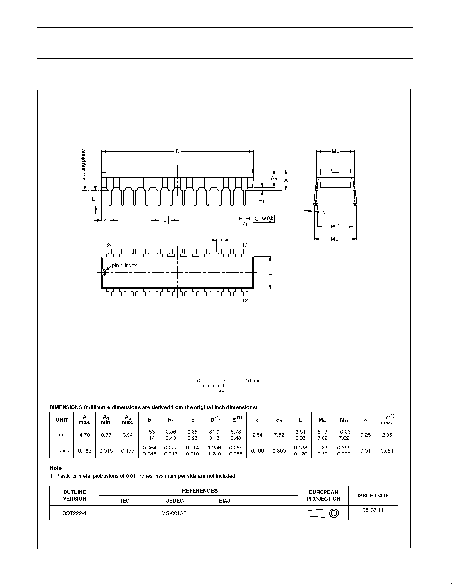
DIP24:
plastic dual in-line package; 24 leads (300 mil)
SOT222-1
Philips Semiconductors
Preliminary specification
83C748/87C748
80C51 8-bit microcontroller family,
2K/64 OTP/ROM, low pin count
1999 Apr 15
15
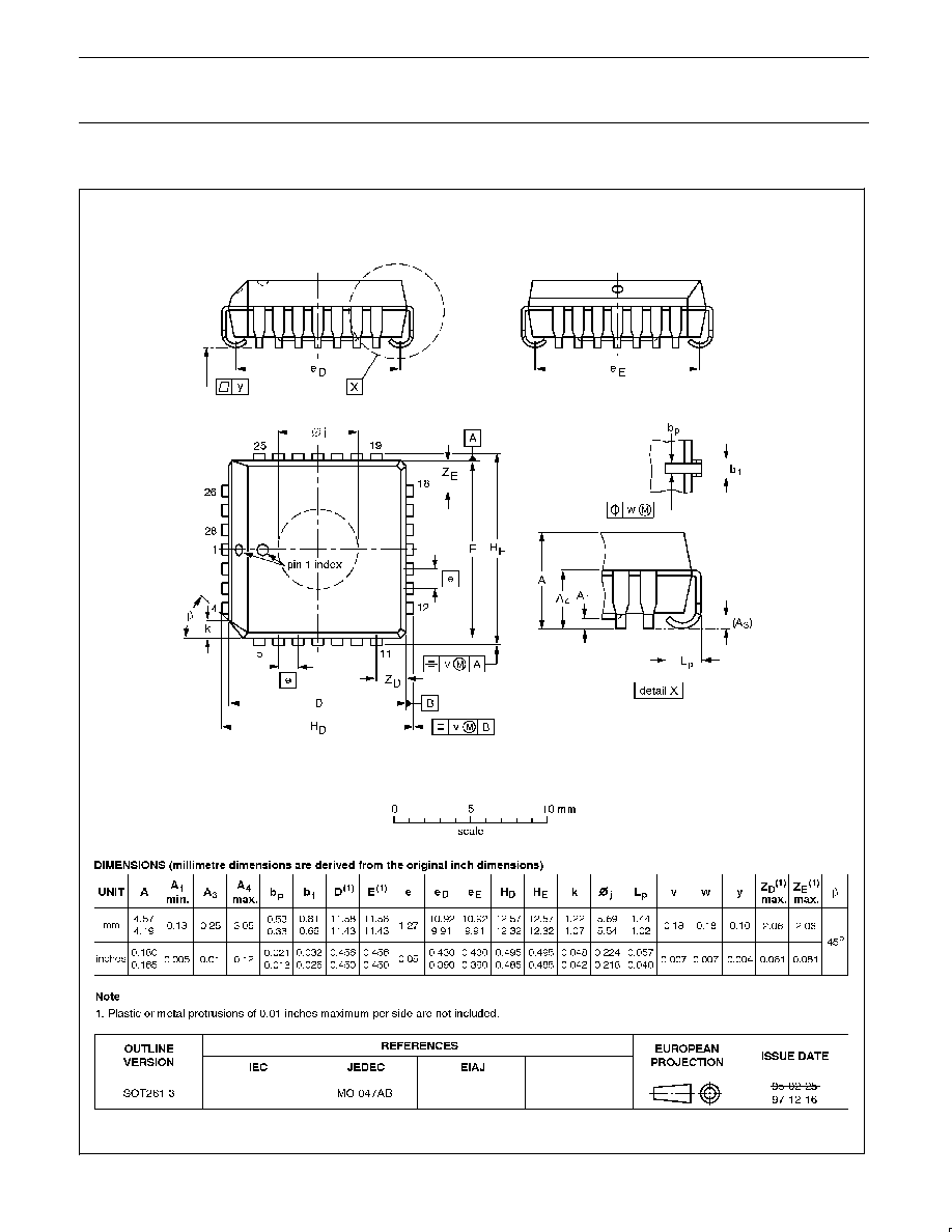
PLCC28:
plastic leaded chip carrer; 28 leads; pedestal
SOT261-3
Philips Semiconductors
Preliminary specification
83C748/87C748
80C51 8-bit microcontroller family,
2K/64 OTP/ROM, low pin count
1999 Apr 15
16
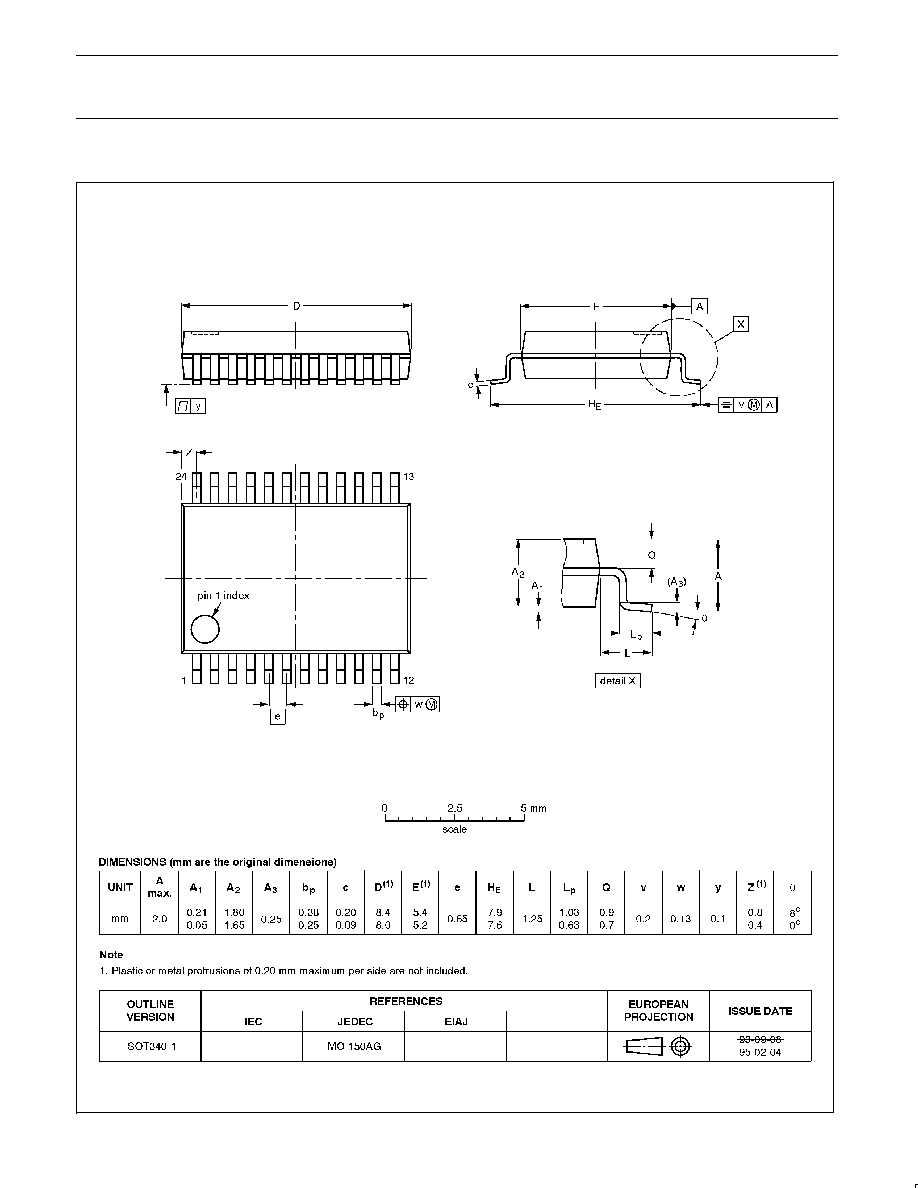
SSOP24:
plastic shrink small outline package; 24 leads; body width 5.3 mm
SOT340-1

Philips Semiconductors
Preliminary specification
83C748/87C748
80C51 8-bit microcontroller family,
2K/64 OTP/ROM, low pin count
1999 Apr 15
17
NOTES

Philips Semiconductors
Preliminary specification
83C748/87C748
80C51 8-bit microcontroller family,
2K/64 OTP/ROM, low pin count
1999 Apr 15
18
Definitions
Short-form specification -- The data in a short-form specification is extracted from a full data sheet with the same type number and title. For
detailed information see the relevant data sheet or data handbook.
Limiting values definition -- Limiting values given are in accordance with the Absolute Maximum Rating System (IEC 134). Stress above one
or more of the limiting values may cause permanent damage to the device. These are stress ratings only and operation of the device at these or
at any other conditions above those given in the Characteristics sections of the specification is not implied. Exposure to limiting values for extended
periods may affect device reliability.
Application information -- Applications that are described herein for any of these products are for illustrative purposes only. Philips
Semiconductors make no representation or warranty that such applications will be suitable for the specified use without further testing or
modification.
Disclaimers
Life support -- These products are not designed for use in life support appliances, devices or systems where malfunction of these products can
reasonably be expected to result in personal injury. Philips Semiconductors customers using or selling these products for use in such applications
do so at their own risk and agree to fully indemnify Philips Semiconductors for any damages resulting from such application.
Right to make changes -- Philips Semiconductors reserves the right to make changes, without notice, in the products, including circuits, standard
cells, and/or software, described or contained herein in order to improve design and/or performance. Philips Semiconductors assumes no
responsibility or liability for the use of any of these products, conveys no license or title under any patent, copyright, or mask work right to these
products, and makes no representations or warranties that these products are free from patent, copyright, or mask work right infringement, unless
otherwise specified.
Philips Semiconductors
811 East Arques Avenue
P.O. Box 3409
Sunnyvale, California 94088≠3409
Telephone 800-234-7381
©
Copyright Philips Electronics North America Corporation 1999
All rights reserved. Printed in U.S.A.
Date of release: 04-99
Document order number:
9397 750 05736
Philips
Semiconductors
Data sheet
status
Objective
specification
Preliminary
specification
Product
specification
Product
status
Development
Qualification
Production
Definition
[1]
This data sheet contains the design target or goal specifications for product development.
Specification may change in any manner without notice.
This data sheet contains preliminary data, and supplementary data will be published at a later date.
Philips Semiconductors reserves the right to make chages at any time without notice in order to
improve design and supply the best possible product.
This data sheet contains final specifications. Philips Semiconductors reserves the right to make
changes at any time without notice in order to improve design and supply the best possible product.
Data sheet status
[1]
Please consult the most recently issued datasheet before initiating or completing a design.