 | –≠–ª–µ–∫—Ç—Ä–æ–Ω–Ω—ã–π –∫–æ–º–ø–æ–Ω–µ–Ω—Ç: 83C752 | –°–∫–∞—á–∞—Ç—å:  PDF PDF  ZIP ZIP |

Philips
Semiconductors
83C752/87C752
80C51 8-bit microcontroller family
2K/64 OTP/ROM, 5 channel 8 bit A/D, I
2
C, PWM,
low pin count
Product specification
Supersedes data of 1998 Jan 19
IC20 Data Handbook
1998 May 01
INTEGRATED CIRCUITS
Philips Semiconductors
Product specification
83C752/87C752
80C51 8-bit microcontroller family
2K/64 OTP/ROM, 5 channel 8 bit A/D, I
2
C, PWM, low pin count
2
1998 May 01
853-1443 19328
DESCRIPTION
The Philips 83C752/87C752 offers many of the advantages of the
80C51 architecture in a small package and at low cost.
The 8XC752 Microcontroller is fabricated with Philips high-density
CMOS technology. Philips epitaxial substrate minimizes CMOS
latch-up sensitivity.
The 8XC752 contains a 2k
◊
8 ROM (83C752) EPROM (87C752), a
64
◊
8 RAM, 21 I/O lines, a 16-bit auto-reload counter/timer, a
fixed-priority level interrupt structure, a bidirectional inter-integrated
circuit (I
2
C) serial bus interface, an on-chip oscillator, a five channel
multiplexed 8-bit A/D converter, and an 8-bit PWM output.
The onboard inter-integrated circuit (I
2
C) bus interface allows the
8XC752 to operate as a master or slave device on the I
2
C small
area network. This capability facilitates I/O and RAM expansion,
access to EEPROM, processor-to-processor communication, and
efficient interface to a wide variety of dedicated I
2
C peripherals.
The EPROM version of this device, the 87C752, is available in both
quartz-lid erasable and plastic one-time programmable (OTP)
packages. Once the array has been programmed, it is functionally
equivalent to the masked ROM 83C752. Thus, unless explicitly
stated otherwise, all references made to the 83C752 apply equally
to the 87C752.
The 83C752 supports two power reduction modes of operation
referred to as the idle mode and the power-down mode.
FEATURES
∑
Available in erasable quartz lid or One-Time Programmable plastic
packages
∑
80C51 based architecture
∑
Inter-integrated Circuit (I
2
C) serial bus interface
∑
Small package sizes
≠ 28-pin DIP
≠ 28-pin PLCC
≠ 28-pin SSOP
∑
Wide oscillator frequency range
∑
Low power consumption:
≠ Normal operation: less than 11mA @ 5V, 12MHz
≠ Idle mode
≠ Power-down mode
∑
2k
◊
8 ROM (83C752)
EPROM (87C752)
∑
64
◊
8 RAM
∑
16-bit auto reloadable counter/timer
∑
5-channel 8-bit A/D converter
∑
8-bit PWM output/timer
∑
Fixed-rate timer
∑
Boolean processor
∑
CMOS and TTL compatible
∑
Well suited for logic replacement, consumer and industrial
applications
PART NUMBER SELECTION
ROM
EPROM
TEMPERATURE RANGE
∞
C
AND PACKAGE
FREQUENCY
DRAWING
NUMBER
S83C752≠1DB
S87C752≠1DB
OTP
0 to +70, 28-pin Plastic Shrink Small Outline Package
3.5 to 12MHz
SOT341-1
S83C752≠1N28
S87C752≠1N28
OTP
0 to +70, 28-pin Plastic Dual In-line Package
3.5 to 12MHz
SOT117-2
S83C752≠2N28
S87C752≠2N28
OTP
≠40 to +85, 28-pin Plastic Dual In-line Package
3.5 to 12MHz
SOT117-2
S83C752≠4DB
S87C752≠4DB
OTP
0 to +70, 28-pin Plastic Shrink Small Outline Package
3.5 to 16MHz
SOT341-1
S83C752≠4N28
S87C752≠4N28
OTP
0 to +70, 28-pin Plastic Dual In-line Package
3.5 to 16MHz
SOT117-2
S83C752≠5N28
S87C752≠5N28
OTP
≠40 to +85, 28-pin Plastic Dual In-line Package
3.5 to 16MHz
SOT117-2
S83C752≠1A28
S87C752≠1A28
OTP
0 to +70, 28-pin Plastic Leaded Chip Carrier
3.5 to 12MHz
SOT261-3
S83C752≠2A28
S87C752≠2A28
OTP
≠40 to +85, 28-pin Plastic Leaded Chip Carrier
3.5 to 12MHz
SOT261-3
S83C752≠4A28
S87C752≠4A28
OTP
0 to +70, 28-pin Plastic Leaded Chip Carrier
3.5 to 16MHz
SOT261-3
S83C752≠5A28
S87C752≠5A28
OTP
≠40 to +85, 28-pin Plastic Leaded Chip Carrier
3.5 to 16MHz
SOT261-3
S83C752≠6A28
S87C752≠6A28
OTP
≠55 to +125, 28-pin Plastic Leaded Chip Carrier
3.5 to 12MHz
SOT261-3
S83C752≠6N28
S87C752≠6N28
OTP
≠55 to +125, 28-pin Plastic Dual In-line Package
3.5 to 12MHz
SOT117-2
NOTE:
1. OTP = One Time Programmable EPROM.
Philips Semiconductors
Product specification
83C752/87C752
80C51 8-bit microcontroller family
2K/64 OTP/ROM, 5 channel 8 bit A/D, I
2
C, PWM, low pin count
1998 May 01
3
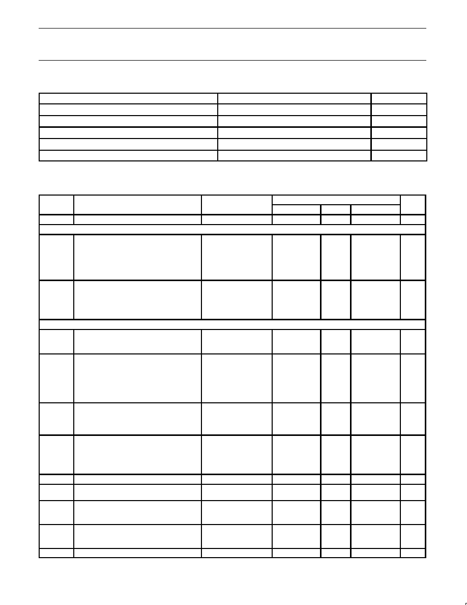
BLOCK DIAGRAM
RST
X1
X2
V
CC
V
SS
RAM
ROM/
EPROM
ACC
TMP2
TMP1
ALU
INSTRUCTION
REGISTER
PD
OSCILLATOR
PSW
BUFFER
DPTR
PCON
I2CFG I2STA
TCON
I2DAT
I2CON
IE
TH0
TL0
RTH
RTL
INTERRUPT, SERIAL
PORT AND TIMER BLOCKS
I
2
C
CONTROL
PWM
P1.0≠P1.7
P3.0≠P3.7
P0.0≠P0.4
ADC
AV
SS
AV
CC
PORT 0
DRIVERS
RAM ADDR
REGISTER
PORT 0
LATCH
PORT 2
LATCH
STACK
POINTER
PROGRAM
ADDRESS
REGISTER
PC
INCRE-
MENTER
PROGRAM
COUNTER
PORT 3
DRIVERS
PORT 1
DRIVERS
PORT 3
LATCH
PORT 1
LATCH
TIMING
AND
CONTROL
B
REGISTER
SU00319

Philips Semiconductors
Product specification
83C752/87C752
80C51 8-bit microcontroller family
2K/64 OTP/ROM, 5 channel 8 bit A/D, I
2
C, PWM, low pin count
1998 May 01
4
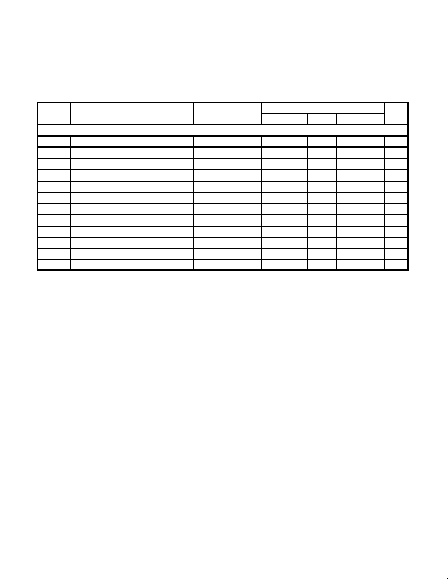
PIN CONFIGURATIONS
1
2
3
4
5
6
7
8
9
10
11
12
14
13
15
16
17
18
19
20
21
22
23
24
P3.4/A4
P3.3/A3
P3.2/A2/A10
P3.1/A1/A9
P3.0/A0/A8
P0.2/V
PP
RST
X2
X1
V
SS
P0.0/SCL/ASEL
P1.4/ADC4/D4
AV
SS
AV
CC
P1.5/INT0/D5
P1.6/INT1/D6
P1.7/T0/D7
P0.3
P0.4/PWM OUT
P3.7/A7
P3.6/A6
P3.5/A5
V
CC
PLASTIC
DUAL
IN-LINE
PACKAGE
AND
SHRINK
SMALL
OUTLINE
PACKAGE
PLASTIC
LEADED
CHIP
CARRIER
4
1
26
5
11
25
19
12
18
P0.1/SDA/OE≠PGM
25
26
27
28
P1.0/ADC0/D0
P1.1/ADC1/D1
P1.3/ADC3/D3
P1.2/ADC2/D2
Pin
Function
1
P3.4/A4
2
P3.3/A3
3
P3.2/A2/A10
4
P3.1/A1/A9
5
P3.0/A0/A8
6
P0.2/V
PP
7
P0.1/SDA/OE-PGM
8
P0.0/SCL/ASEL
9
RST
10
X2
11
X1
12
V
SS
13
P1.0/ADC0/D0
14
P1.1/ADC1/D1
Pin
Function
15
P1.2/ADC2/D2
16
P1.3/ADC3/D3
17
P1.4/ADC4/D4
18
AV
SS
19
AV
CC
20
P1.5/INT0/D5
21
P1.6/INT1/D6
22
P1.7/T0/D7
23
P0.3
24
P0.4/PWM OUT
25
P3.7/A7
26
P3.6/A6
27
P3.5/A5
28
V
CC
SU00318

Philips Semiconductors
Product specification
83C752/87C752
80C51 8-bit microcontroller family
2K/64 OTP/ROM, 5 channel 8 bit A/D, I
2
C, PWM, low pin count
1998 May 01
5
PIN DESCRIPTION
MNEMONIC
PIN NO.
TYPE
NAME AND FUNCTION
V
SS
12
I
Circuit Ground Potential.
V
CC
28
I
Supply voltage during normal, idle, and power-down operation.
P0.0≠P0.4
8≠6
23, 24
I/O
Port 0: Port 0 is a 5-bit bidirectional port. Port 0.0≠P0.2 are open drain. Port 0.0≠P0.2 pins that have
1s written to them float, and in that state can be used as high-impedance inputs. P0.3≠P0.4 are
bidirectional I/O port pins with internal pull-ups. Port 0 also serves as the serial I
2
C interface. When this
feature is activated by software, SCL and SDA are driven low in accordance with the I
2
C protocol.
These pins are driven low if the port register bit is written with a 0 or if the I
2
C subsystem presents a 0.
The state of the pin can always be read from the port register by the program. Port 0.3 and 0.4 have
internal pull-ups that function identically to port 3. Pins that have 1s written to them are pulled high by
the internal pull-ups and can be used as inputs.
To comply with the I
2
C specification, P0.0 and P0.1 are open drain bidirectional I/O pins with the
electrical characteristics listed in the tables that follow. While these differ from "standard TTL"
characteristics, they are close enough for the pins to still be used as general-purpose I/O in non-I
2
C
applications.
6
I
V
PP
(P0.2) ≠ Programming voltage input. (See Note 2.)
7
I
OE/PGM (P0.1) ≠ Input which specifies verify mode (output enable) or the program mode.
OE/PGM = 1 output enabled (verify mode).
OE/PGM = 0 program mode.
8
I
ASEL (P0.0) ≠ Input which indicates which bits of the EPROM address are applied to port 3.
ASEL = 0 low address byte available on port 3.
ASEL = 1 high address byte available on port 3 (only the three least significant bits are used).
P1.0≠P1.7
13≠17,
20≠22
I/O
Port 1: Port 1 is an 8-bit bidirectional I/O port with internal pull-ups. Port 1 pins that have 1s written to
them are pulled high by the internal pull-ups and can be used as inputs. P0.3≠P0.4 pins are
bidirectional I/O port pins with internal pull-ups. As inputs, port 1 pins that are externally pulled low will
source current because of the internal pull-ups. (See DC Electrical Characteristics: I
IL
). Port 1 also
serves the special function features of the SC80C51 family as listed below:
20
I
INT0 (P1.5): External interrupt.
21
I
INT1 (P1.6): External interrupt.
22
I
T0 (P1.7): Timer 0 external input.
13≠17
I
ADC0 (P1.0)≠ADC4 (P1.4): Port 1 also functions as the inputs to the five channel multiplexed A/D
converter. These pins can be used as outputs only if the A/D function has been disabled. These pins
can be used as inputs while the A/D converter is enabled.
Port 1 serves to output the addressed EPROM contents in the verify mode and accepts as inputs the
value to program into the selected address during the program mode.
P3.0≠P3.7
5≠1,
27≠25
I/O
Port 3: Port 3 is an 8-bit bidirectional I/O port with internal pull-ups. Port 3 pins that have 1s written to
them are pulled high by the internal pull-ups and can be used as inputs. As inputs, port 3 pins that are
externally being pulled low will source current because of the pull-ups. (See DC Electrical
Characteristics: I
IL
). Port 3 also functions as the address input for the EPROM memory location to be
programmed (or verified). The 11-bit address is multiplexed into this port as specified by P0.0/ASEL.
RST
9
I
Reset: A high on this pin for two machine cycles while the oscillator is running resets the device. An
internal diffused resistor to V
SS
permits a power-on RESET using only an external capacitor to V
CC
.
After the device is reset, a 10-bit serial sequence, sent LSB first, applied to RESET, places the device
in the programming state allowing programming address, data and V
PP
to be applied for programming
or verification purposes. The RESET serial sequence must be synchronized with the X1 input.
X1
11
I
Crystal 1: Input to the inverting oscillator amplifier and input to the internal clock generator circuits. X1
also serves as the clock to strobe in a serial bit stream into RESET to place the device in the
programming state.
X2
10
O
Crystal 2: Output from the inverting oscillator amplifier.
AV
CC
1
19
I
Analog supply voltage and reference input.
AV
SS
1
18
I
Analog supply and reference ground.
NOTE:
1. AV
SS
(reference ground) must be connected to 0V (ground). AV
CC
(reference input) cannot differ from V
CC
by more than
±
0.2V, and must be
in the range 4.5V to 5.5V.
2. When P0.2 is at or close to 0V, it may affect the internal ROM operation. We recommend that P0.2 be tied to V
CC
via a small pull-up
(e.g., 2k
).

Philips Semiconductors
Product specification
83C752/87C752
80C51 8-bit microcontroller family
2K/64 OTP/ROM, 5 channel 8 bit A/D, I
2
C, PWM, low pin count
1998 May 01
6
OSCILLATOR CHARACTERISTICS
X1 and X2 are the input and output, respectively, of an inverting
amplifier which can be configured for use as an on-chip oscillator.
To drive the device from an external clock source, X1 should be
driven while X2 is left unconnected. There are no requirements on
the duty cycle of the external clock signal, because the input to the
internal clock circuitry is through a divide-by-two flip-flop. However,
minimum and maximum high and low times specified in the data
sheet must be observed.
IDLE MODE
The 8XC752 includes the 80C51 power-down and idle mode
features. In idle mode, the CPU puts itself to sleep while all of the
on-chip peripherals except the A/D and PWM stay active. The
functions that continue to run while in the idle mode are Timer 0, the
I
2
C interface including Timer I, and the interrupts. The instruction to
invoke the idle mode is the last instruction executed in the normal
operating mode before the idle mode is activated. The CPU
contents, the on-chip RAM, and all of the special function registers
remain intact during this mode. The idle mode can be terminated
either by any enabled interrupt (at which time the process is picked
up at the interrupt service routine and continued), or by a hardware
reset which starts the processor in the same manner as a power-on
reset. Upon powering-up the circuit, or exiting from idle mode,
sufficient time must be allowed for stabilization of the internal analog
reference voltages before an A/D conversion is started.
Special Function Registers
The special function registers (directly addressable only) contain all
of the 8XC751 registers except the program counter and the four
register banks. Most of the 21 special function registers are used to
control the on-chip peripheral hardware. Other registers include
arithmetic registers (ACC, B, PSW), stack pointer (SP) and data
pointer registers (DPH, DPL). Nine of the SFRs are bit addressable.
Data Pointer
The data pointer (DPTR) consists of a high byte (DPH) and a low
byte (DPL). In the 80C51 this register allows the access of external
data memory using the MOVX instruction. Since the 83C752 does
not support MOVX or external memory accesses, this register is
generally used as a 16-bit offset pointer of the accumulator in a
MOVC instruction. DPTR may also be manipulated as two
independent 8-bit registers.
POWER-DOWN MODE
In the power-down mode, the oscillator is stopped and the instruction
to invoke power-down is the last instruction executed. Only the
contents of the on-chip RAM are preserved. A hardware reset is the
only way to terminate the power-down mode. The control bits for the
reduced power modes are in the special function register PCON.
Table 1. External Pin Status During Idle and
Power-Down Modes
MODE
Port 0*
Port 1
Port 2
Idle
Data
Data
Data
Power-down
Data
Data
Data
*
Except for PWM output (P0.4).
DIFFERENCES BETWEEN THE 8XC752 AND
THE 80C51
Program Memory
On the 8XC752, program memory is 2048 bytes long and is not
externally expandable, so the 80C51 instructions MOVX, LJMP, and
LCALL are not implemented. If these instructions are executed, the
appropriate number of instruction cycles will take place along with
external fetches; however, no operation will take place. The LJMP
may not respond to all program address bits. The only fixed
locations in program memory are the addresses at which execution
is taken up in response to reset and interrupts, which are as follows:
Program Memory
Event
Address
Reset
000
External INT0
003
Counter/timer 0
00B
External INT1
013
Timer I
01B
I
2
C serial
023
ADC
02B
PWM
033
Memory Organization
The 8XC752 manipulates operands in three memory address
spaces. The first is the program memory space which contains
program instructions as well as constants such as look-up tables.
The program memory space contains 2k bytes in the 8XC752.
The second memory space is the data memory array which has a
logical address space of 128 bytes. However, only the first 64 (0 to
3FH) are implemented in the 8XC752.
The third memory space is the special function register array having
a 128-byte address space (80H to FFH). Only selected locations in
this memory space are used (see Table 2). Note that the
architecture of these memory spaces (internal program memory,
internal data memory, and special function registers) is identical to
the 80C51, and the 8XC752 varies only in the amount of memory
physically implemented.
The 8XC752 does not directly address any external data or program
memory spaces. For this reason, the MOVX instructions in the
80C51 instruction set are not implemented in the 83C752, nor are
the alternate I/O pin functions RD and WR.
Philips Semiconductors
Product specification
83C752/87C752
80C51 8-bit microcontroller family
2K/64 OTP/ROM, 5 channel 8 bit A/D, I
2
C, PWM, low pin count
1998 May 01
7
P1.X
LATCH
D
Q
CL
Q
READ
LATCH
INT. BUS
WRITE TO
LATCH
READ
PIN
ALTERNATE INPUT
FUNCTION
VDD
P1.X
PIN
INTERNAL
PULL-UP
ALTERNATE
OUTPUT
FUNCTION
P0.X
LATCH
D
Q
CL
Q
READ
LATCH
INT. BUS
WRITE TO
LATCH
READ
PIN
ALTERNATE INPUT
FUNCTION
P0.X
PIN
ALTERNATE
OUTPUT
FUNCTION
SU00306
Figure 1. Port Bit Latches and I/O Buffers
I/O Ports
The I/O pins provided by the 83C752 consist of port 0, port 1, and
port 3.
Port 0
Port 0 is a 5-bit bidirectional I/O port and includes alternate functions
on some pins of this port. Pins P0.3 and P0.4 are provided with
internal pullups while the remaining pins (P0.0, P0.1, and P0.2) have
open drain output structures. The alternate functions for port 0 are:
P0.0
SCL ≠ the I
2
C bus clock
P0.1
SDA ≠ the I
2
C bus data
P0.4
PWM ≠ the PWM output
If the alternate functions, I
2
C and PWM, are not being used, then
these pins may be used as I/O ports.
Port 1
Port 1 is an 8-bit bidirectional I/O port whose structure is identical to
the 80C51, but also includes alternate input functions on all pins.
The alternate pin functions for port 1 are:
P1.0-P1.4 - ADC0-ADC4 - A/D converter analog inputs
P1.5 INT0 - external interrupt 0 input
P1.6 INT1 - external interrupt 1 input
P1.7 - T0 - timer 0 external input
If the alternate functions INT0, INT1, or T0 are not being used, these
pins may be used as standard I/O ports. It is necessary to connect
AV
CC
and AV
SS
to V
CC
and V
SS
, respectively, in order to use these
pins as standard I/O pins. When the A/D converter is enabled, the
analog channel connected to the A/D may not be used as a digital
input; however, the remaining analog inputs may be used as digital
inputs. They may not be used as digital outputs. While the A/D is
enabled, the analog inputs are floating.
Port 3
Port 3 is an 8-bit bidirectional I/O port whose structure is identical to
the 80C51. Note that the alternate functions associated with port 3
of the 80C51 have been moved to port 1 of the 83C752 (as
applicable). See Figure 1 for port bit configurations.
Counter/Timer Subsystem
The 8XC752 has one counter/timer called timer/counter 0. Its
operation is similar to mode 2 operation on the 80C51, but is
extended to 16 bits with 16 bits of autoload. The controls for this
counter are centralized in a single register called TCON.
A watchdog timer, called Timer I, is for use with the I
2
C subsystem.
In I
2
C applications, this timer is dedicated to time-generation and
bus monitoring of the I
2
C. In non-I
2
C applications, it is available for
use as a fixed time-base.
Interrupt Subsystem--Fixed Priority
The IP register and the 2-level interrupt system of the 80C51 are
eliminated. The interrupt structure is a seven-source, one-level
interrupt system similar to the 8XC751. Simultaneous interrupt
conditions are resolved by a single-level, fixed priority as follows:
Highest priority:
Pin INT0
Counter/timer flag 0
Pin INT1
PWM
Timer I
Serial I
2
C
Lowest priority:
ADC
The vector addresses are as follows:
Source
Vector Address
INT0
0003H
TF0
000BH
INT1
0013H
TIMER I
001BH
SIO
0023H
ADC
002BH
PWM
0033H
Interrupt Control Registers
The 80C51 interrupt enable register is modified to take into account
the different interrupt sources of the 8XC752.

Philips Semiconductors
Product specification
83C752/87C752
80C51 8-bit microcontroller family
2K/64 OTP/ROM, 5 channel 8 bit A/D, I
2
C, PWM, low pin count
1998 May 01
8
Interrupt Enable Register
MSB
LSB
EA
EAD
ETI
ES
EPWM
EX1
ET0
EX0
Position Symbol
Function
IE.7
EA
Global interrupt disable when EA = 0
IE.6
EAD
A/D conversion complete
IE.5
ETI
Timer I
IE.4
ES
I
2
C serial port
IE.3
EPWM
PWM counter overflow
IE.2
EX1
External interrupt 1
IE.1
ET0
Timer 0 overflow
IE.0
EX0
External interrupt 0
Serial Communications
The 8XC752 contains an I
2
C serial communications port instead of
the 80C51 UART. The I
2
C serial port is a single bit hardware
interface with all of the hardware necessary to support multimaster
and slave operations. Also included are receiver digital filters and
timer (timer I) for communication watch-dog purposes. The I
2
C
serial port is controlled through four special function registers; I
2
C
control, I
2
C data, I
2
C status, and I
2
C configuration.
The I
2
C bus uses two wires (SDA and SCL) to transfer information
between devices connected to the bus. The main technical features
of the bus are:
∑
Bidirectional data transfer between masters and slaves
∑
Serial addressing of slaves
∑
Acknowledgment after each transferred byte
∑
Multimaster bus
∑
Arbitration between simultaneously transmitting master without
corruption of serial data on bus
∑
With 82B715, communication distance is extended to beyond 100
feet (30M)
A large family of I
2
C compatible ICs is available. See the I
2
C section
for more details on the bus and available ICs.
The 83C752 I
2
C subsystem includes hardware to simplify the
software required to drive the I
2
C bus. This circuitry is the same as
that on the 83C751. (See the 83C751 section for a detailed
discussion of this subsystem).
Pulse Width Modulation Output (P0.4)
The PWM outputs pulses of programmable length and interval. The
repetition frequency is defined by an 8-bit prescaler which generates
the clock for the counter. The prescaler register is PWMP. The
prescaler and counter are not associated with any other timer. The
8-bit counter counts modulo 255, that is from 0 to 254 inclusive. The
value of the 8-bit counter is compared to the contents of a compare
register, PWM. When the counter value matches the contents of this
register, the output of the PWM is set high. When the counter reaches
zero, the output of the PWM is set low. The pulse width ratio (duty
cycle) is defined by the contents of the compare register and is in the
range of 0 to 1 programmed in increments of 1/255. The PWM output
can be set to be continuously high by loading the compare register
with 0 and the output can be set to be continuously low by loading the
compare register with 255. The PWM output is enabled by a bit in a
special function register, PWENA. When enabled, the pin output is
driven with a fully active pull-up. That is, when the output is high, a
strong pull-up is continuously applied. when disabled, the pin
functions as a normal bidirectional I/O pin, however, the counter
remains active.
The PWM function is disabled during RESET and remains disabled
after reset is removed until re-enabled by software. The PWM output
is high during power down and idle. The counter is disabled during
idle. The repetition frequency of the PWM is given by:
f
PWM
= f
OSC
/ 2 (1 + PWMP) 255
The low/high ratio of the PWM signal is PWM / (255 ≠ PWM) for
PWM not equal to 255. For PWM = 255, the output is always low.
The repetition frequency range is 92Hz to 23.5kHz for an oscillator
frequency of 12MHz.
An interrupt will be asserted upon PWM counter overflow if the
interrupt is not masked off.
The PWM output is an alternative function of P0.4. In order to use
this port as a bidirectional I/O port, the PWM output must be
disabled by clearing the enable/disable bit in PWENA. In this case,
the PWM subsystem can be used as an interval timer by enabling
the PWM interrupt.

Philips Semiconductors
Product specification
83C752/87C752
80C51 8-bit microcontroller family
2K/64 OTP/ROM, 5 channel 8 bit A/D, I
2
C, PWM, low pin count
1998 May 01
9
Table 2.
8XC752 Special Function Registers
SYMBOL
DESCRIPTION
DIRECT
ADDRESS
BIT ADDRESS, SYMBOL, OR ALTERNATIVE PORT FUNCTION
MSB
LSB
RESET
VALUE
ACC*
Accumulator
E0H
E7
E6
E5
E4
E3
E2
E1
E0
00H
ADAT#
A/D result
84H
00H
ADCON#
A/D control
A0H
≠
≠
ENADC
ADCI
ADCS
AADR2
AADR1
AADR0
C0H
B*
B register
F0H
F7
F6
F5
F4
F3
F2
F1
F0
00H
DPTR:
DPL
DPH
Data pointer
(2 bytes)
Data pointer low
Data pointer high
82H
83H
00H
00H
DF
DE
DD
DC
DB
DA
D9
D8
I
2
CFG*#
I
2
C configuration
D8H/RD
SLAVEN
MASTRQ
0
TIRUN
≠
≠
CT1
CT0
0000xx00B
WR
SLAVEN
MASTRQ
CLRTI
TIRUN
≠
≠
CT1
CT0
9F
9E
9D
9C
9B
9A
99
98
I
2
CON*#
I
2
C control
98H/RD
RDAT
ATN
DRDY
ARL
STR
STP
MASTER
≠
81H
WR
CXA
IDLE
CDR
CARL
CSTR
CSTP
XSTR
XSTP
I
2
DAT#
I
2
C data
99H/RD
RDAT
0
0
0
0
0
0
0
80H
WR
XDAT
X
X
X
X
X
X
X
FF
FE
FD
FC
FB
FA
F9
F8
I
2
STA*#
I
2
C status
F8H
≠
IDLE
XDATA
XACTV
MAKSTR
MAKSTP
XSTR
XSTP
x0100000B
AF
AE
AD
AC
AB
AA
A9
A8
IE*#
Interrupt enable
ADH
EA
EAD
ETI
ES
EPWM
EX1
ET0
EX0
00H
≠
≠
≠
84
83
82
81
80
xxx11111B
P0*#
Port 0
80H
≠
≠
≠
PWM0
≠
≠
SDA
SCL
97
96
95
94
93
92
91
90
FFH
P1*#
Port 1
90H
T0
INT1
INT0
ADC4
ADC3
ADC2
ADC1
ADC0
P3*
Port 3
B0H
B7
B6
B5
B4
B3
B2
B1
B0
FFH
PCON#
Power control
87H
≠
≠
≠
≠
≠
≠
PD
IDL
xxxx0000B
D7
D6
D5
D4
D3
D2
D1
D0
PSW*
Program status word
D0H
CY
AC
F0
RS1
RS0
OV
≠
P
00H
PWCM#
PWM compare
8EH
xxxxxxxxB
PWENA#
PWM enable
FEH
≠
≠
≠
≠
≠
≠
≠
PWE
FEH
PWMP#
PWM prescaler
8FH
00H
RTL#
Timer low reload
8BH
00H
RTH#
Timer high reload
8DH
00H
SP
Stack pointer
81H
07H
TL#
Timer low
8AH
00H
TH#
Timer high
8CH
00H
8F
8E
8D
8C
8B
8A
89
88
TCON*#
Timer control
88H
GATE
C/T
TF
TR
IE0
IT0
IE1
IT1
00H
*
SFRs are bit addressable.
#
SFRs are modified from or added to the 80C51 SFRs.
Philips Semiconductors
Product specification
83C752/87C752
80C51 8-bit microcontroller family
2K/64 OTP/ROM, 5 channel 8 bit A/D, I
2
C, PWM, low pin count
1998 May 01
10
Special Function Register Addresses
Special function registers for the 8XC752 are identical to those of
the 80C51, except for the changes listed below:
80C51 special function registers not present in the 8XC752 are
TMOD (89), P2 (A0) and IP (B8). The 80C51 registers TH1, TL1,
SCON, and SBUF are replaced with the 8XC752 registers RTH,
RTL, I2CON, and I2DAT, respectively. Additional special function
registers are I2CFG (D8) and I2STA (FB), ADCON (A0), ADAT (84),
PWM (8E), PWMP (8F), and PWENA (FE). See Table 3.
A/D Converter
The analog input circuitry consists of a 5-input analog multiplexer and
an A to D converter with 8-bit resolution. The conversion takes 40
machine cycles, i.e., 40
µ
s at 12MHz oscillator frequency. The A/D
converter is controlled using the ADCON control register. Input
channels are selected by the analog multiplexer through ADCON
register bits 0≠2.
The 83C752 contains a five-channel multiplexed 8-bit A/D converter.
The conversion requires 40 machine cycles (40
µ
s at 12MHz
oscillator frequency).
The A/D converter is controlled by the A/D control register, ADCON.
Input channels are selected by the analog multiplexer by bits
ADCON.0 through ADCON.2. The ADCON register is not bit
addressable.
ADCON Register
MSB
LSB
X
X
ENADC
ADCI
ADCS
AADR2
AADR1
AADR0
ADCI
ADCS
Operation
0
0
ADC not busy, a conversion can be started.
0
1
ADC busy, start of a new conversion is blocked.
1
0
Conversion completed, start of a new conversion is
blocked.
1
1
Not possible.
INPUT CHANNEL SELECTION
ADDR2
ADDR1
ADDR0
INPUT PIN
0
0
0
P1.0
0
0
1
P1.1
0
1
0
P1.2
0
1
1
P1.3
1
0
0
P1.4
Position
Symbol
Function
ADCON.5
ENADC
Enable A/D function when ENADC = 1. Reset
forces ENADC = 0.
ADCON.4
ADCI
ADC interrupt flag. This flag is set when an
ADC conversion is complete. If IE.6 = 1, an
interrupt is requested when ADCI = 1. The
ADCI flag is cleared when conversion data is
read. This flag is read only.
ADCON.3
ADCS
ADC start. Setting this bit starts an A/D
conversion. Once set, ADCS remains high
throughout the conversion cycle. On
completion of the conversion, it is reset just
before the ADCI interrupt flag is cleared.
ADCS cannot be reset by software. ADCS
should not be used to monitor the A/D
converter status. ADCI should be used for this
purpose.
ADCON.2
AADR2
Analog input select.
ADCON.1
AADR1
Analog input select.
ADCON.0
AADR0
Analog input select. This binary coded
address selects one of the five analog input
port pins of P1 to be input to the converter. It
can only be changed when ADCI and ADCS
are both low. AADR2 is the most significant
bit.
The completion of the 8-bit ADC conversion is flagged by ADCI in
the ADCON register, and the result is stored in the special function
register ADAT.
An ADC conversion in progress is unaffected by an ADC start. The
result of a completed conversion remains unaffected provided ADCI
remains at a logic 1. While ADCS is a logic 1 or ADCI is a logic 1, a
new ADC START will be blocked and consequently lost. An ADC
conversion in progress is aborted when the idle or power-down
mode is entered. The result of a completed conversion (ADCI = logic
1) remains unaffected when entering the idle mode. See Figure 2 for
an A/D input equivalent circuit.
The analog input pins ADC0-ADC4 may be used as digital inputs
and outputs when the A/D converter is disabled by a 0 in the
ENADC bit in ADCON. When the A/D is enabled, the analog input
channel that is selected by the ADDR2-ADDR0 bits in ADCON
cannot be used as a digital input. Reading the selected A/D channel
as a digital input will always return a 1. The unselected A/D inputs
may always be used as digital inputs. Unselected analog inputs will
be floating and may not be used as digital outputs.
The A/D reference inputs on the 8XC752 are tied together with the
analog supply pins AV
CC
and AV
SS
. This means that the reference
voltage on the A/D cannot be varied separately from the analog
supply pins. AV
SS
must be connected to 0V and AV
CC
must be
connected to a supply voltage between 4.5V and 5.5V. A/D
measurements may be made in the range of 4.5V to 5.5V.
Increasing the voltage on the A/D ground reference above 0V or
reducing the voltage on the positive A/D reference below 4.5V is not
permitted.

Philips Semiconductors
Product specification
83C752/87C752
80C51 8-bit microcontroller family
2K/64 OTP/ROM, 5 channel 8 bit A/D, I
2
C, PWM, low pin count
1998 May 01
11
R
S
V
ANALOG
INPUT
C
S
C
C
To Comparator
+
I
N
I
N+1
Sm
N+1
Sm
N
Rm
N+1
Rm
N
Multiplexer
Rm = 0.5 - 3 k
CS + CC = 15pF maximum
RS = Recommended < 9.6 k
for 1 LSB @ 12MHz
NOTE:
Because the analog to digital converter has a sampled-data comparator, the input looks capacitive to a source. When a conversion
is initiated, switch Sm closes for 8tcy (8
µ
s @ 12MHz crystal frequency) during which time capacitance Cs + Cc is charged. It should
be noted that the sampling causes the analog input to present a varying load to an analog source.
SU00199
Figure 2. A/D Input: Equivalent Circuit
A/D CONVERTER PARAMETER DEFINITIONS
The following definitions are included to clarify some specifications
given and do not represent a complete set of A/D parameter
definitions.
Absolute Accuracy Error
Absolute accuracy error of a given output is the difference between
the theoretical analog input voltage to produce a given output and
the actual analog input voltage required to produce the same code.
Since the same output code is produced by a band of input voltages,
the "required input voltage" is defined as the midpoint of the band of
input voltage that will produce that code. Absolute accuracy error
not specified with a code is the maximum over all codes.
Nonlinearity
If a straight line is drawn between the end points of the actual
converter characteristics such that zero offset and full scale errors
are removed, then non-linearity is the maximum deviation of the
code transitions of the actual characteristics from that of the straight
line so constructed. This is also referred to as relative accuracy and
also integral non-linearity.
Differential Non-Linearity
Differential non-linearity is the maximum difference between the
actual and ideal code widths of the converter. The code widths are
the differences expressed in LSB between the code transition
points, as the input voltage is varied through the range for the
complete set of codes.
Gain Error
Gain error is the deviation between the ideal and actual analog input
voltage required to cause the final code transition to a full-scale
output code after the offset error has been removed. This may
sometimes be referred to as full scale error.
Offset Error
Offset error is the difference between the actual input voltage that
causes the first code transition and the ideal value to cause the first
code transition. This ideal value is 1/2 LSB above V
ref≠
.
Channel to Channel Matching
Channel to channel matching is the maximum difference between
the corresponding code transitions of the actual characteristics
taken from different channels under the same temperature, voltage
and frequency conditions.
Crosstalk
Crosstalk is the measured level of a signal at the output of the
converter resulting from a signal applied to one deselected channel.
Total Error
Maximum deviation of any step point from a line connecting the ideal
first transition point to the ideal last transition point.
Relative Accuracy
Relative accuracy error is the deviation of the ADC's actual code
transition points from the ideal code transition points on a straight
line which connects the ideal first code transition point and the final
code transition point, after nullifying offset error and gain error. It is
generally expressed in LSBs or in percent of FSR.

Philips Semiconductors
Product specification
83C752/87C752
80C51 8-bit microcontroller family
2K/64 OTP/ROM, 5 channel 8 bit A/D, I
2
C, PWM, low pin count
1998 May 01
12
COUNTER/TIMER
The 8XC752 counter/timer is designated Timer 0 and is separate
from Timer I of the I
2
C serial port and from the PWM. Its operation is
similar to mode 2 of the 80C51 counter/timer, extended to 16 bits.
When Timer 0 is used in the external counter mode, the T0 input
(P1.7) is sampled every S4P1. The counter/timer function is
controlled using the timer control register (TCON).
TCON Register
MSB
LSB
GATE
C/T
TF
TR
IE0
IT0
IE1
IT1
Position Symbol
Function
TCON.7
GATE
1 ≠ Timer 0 is enabled only when INT0 pin is
high and TR is 1.
0 ≠ Timer 0 is enabled only when TR is 1.
TCON.6
C/T
1 ≠ Counter operation from T0 pin.
0 ≠ Timer operation from internal clock.
TCON.5
TF
1 ≠ Set on overflow of T0.
0 ≠ Cleared when processor vectors to interrupt
routine and by reset.
TCON.4
TR
1 ≠ Enable timer 0
0 ≠ Disable timer 0
TCON.3
IE0
1 ≠ Edge detected on INT0
TCON.2
IT0
1 ≠ INT0 is edge triggered.
0 ≠ INT0 is level sensitive.
TCON.1
IE1
1 ≠ Edge detected on INT1
TCON.0
IT1
1 ≠ INT1 is edge triggered.
0 ≠ INT1 is level sensitive.
These flags are functionally identical to the corresponding 80C51
flags except that there is only one of the 80C51 style timers, and the
flags are combined into one register.
Note that the positions of the IE0/IT0 and IE1/IT1 bits are
transposed from the positions used in the standard 80C51 TCON
register.
A communications watchdog timer, Timer I, is described in the I
2
C
section. In I
2
C applications, this timer is dedicated to time generation
and bus monitoring for the I
2
C. In non-I
2
C applications, it is available
for use as a fixed time base.
The 16-bit timer/counter's operation is similar to mode 2 operation
on the 80C51, but is extended to 16 bits. The timer/counter is
clocked by either 1/12 the oscillator frequency or by transitions on
the T0 pin. The C/T pin in special function register TCON selects
between these two modes. When the TCON TR bit is set, the
timer/counter is enabled. Register pair TH and TL are incremented
by the clock source. When the register pair overflows, the register
pair is reloaded with the values in registers RTH and RTL. The value
in the reload registers is left unchanged. The TF bit in special
function register TCON is set on counter overflow and, if the
interrupt is enabled, will generate an interrupt (see Figure 3).
OSC
˜
12
TL
TH
TF
RTL
RTH
T0 Pin
TR
Gate
INT0 Pin
Int.
C/T = 0
C/T = 1
Reload
SU00300
Figure 3. 83C752 Counter/Timer Block Diagram
Table 3. I
2
C Special Function Register Addresses
REGISTER ADDRESS
BIT ADDRESS
NAME
SYMBOL
ADDRESS
MSB LSB
I
2
C control
I2CON
98
9F
9E
9D
9C
9B
9A
99
98
I
2
C data
I2DAT
99
≠
≠
≠
≠
≠
≠
≠
≠
I
2
C configuration
I2CFG
D8
DF
DE
DD
DC
DB
DA
D9
D8
I
2
C status
I2STA
F8
FF
FE
FD
FC
FB
FA
F9
F8
Philips Semiconductors
Product specification
83C752/87C752
80C51 8-bit microcontroller family
2K/64 OTP/ROM, 5 channel 8 bit A/D, I
2
C, PWM, low pin count
1998 May 01
13
ABSOLUTE MAXIMUM RATINGS
1, 3, 4
PARAMETER
RATING
UNIT
Storage temperature range
≠65 to +150
∞
C
Voltage from V
CC
to V
SS
≠0.5 to +6.5
V
Voltage from any pin to V
SS
(except V
PP
)
≠0.5 to V
CC
+ 0.5
V
Power dissipation
1.0
W
Voltage from V
PP
pin to V
SS
≠0.5 to + 13.0
V
DC ELECTRICAL CHARACTERISTICS
T
amb
= 0
∞
C to +70
∞
C or ≠40
∞
C to +85
∞
C, AV
CC
= 5V
±
5, AV
SS
= 0V
4
V
CC
= 5V
±
10%, V
SS
= 0V
TEST
LIMITS
4
SYMBOL
PARAMETER
CONDITIONS
MIN
Typical
1
MAX
UNIT
I
CC
Supply current (see Figure 6)
Inputs
V
IL
Input low voltage, except SDA, SCL
(0 to 70
∞
C)
(≠40 to +85
∞
C)
≠0.5
≠0.5
0.2V
CC
≠0.1
0.2V
CC
≠0.15
V
V
V
IH
Input high voltage, except X1, RST
(0 to 70
∞
C)
(≠40 to +85
∞
C)
0.2V
CC
+0.9
(0.2V
CC
+1)
V
CC
+0.5
V
CC
+0.5
V
V
V
IH1
Input high voltage, X1, RST
(0 to 70
∞
C)
(≠40 to +85
∞
C)
0.7V
CC
0.7V
CC
to 0.1
V
CC
+0.5
V
CC
+0.5
V
V
SDA, SCL, P0.2
V
IL1
Input low voltage
(0 to 70
∞
C)
(≠40 to +85
∞
C)
≠0.5
≠0.5
0.3V
CC
0.3V
CC
≠0.1
V
V
V
IH2
Input high voltage
(0 to 70
∞
C)
(≠40 to ≠85
∞
C)
0.7V
CC
0.7V
CC
+0.1
V
CC
+0.5
V
CC
+0.5
V
Outputs
V
OL
Output low voltage, ports 1, 3, 0.3, and 0.4
(PWM disabled)
I
OL
= 1.6mA
2
0.45
V
V
OL1
Output low voltage, port 0.2
I
OL
= 3.2mA
2
0.45
V
V
OH
Output high voltage, ports 1, 3, 0.3, and 0.4
(PWM disabled)
I
OH
= ≠60
µ
A,
2.4
V
I
OH
= ≠25
µ
A
0.75V
CC
V
I
OH
= ≠10
µ
A
0.9V
CC
V
I
OH
= ≠400
µ
A
2.4
V
V
OH2
Output high voltage, P0.4 (PWM enabled)
I
OH
= ≠40
µ
A
0.9V
CC
V
Port 0.0 and 0.1 (I
2
C) ≠ Drivers
I
OL
= 3mA
(
V
)
V
OL2
Output low voltage
(over V
CC
range)
0.4
V
C
Driver, receiver combined:
Capacitance
10
pF
I
IL
Logical 0 input current,
ports 1, 3, 0.3, and 0.4 (PWM disabled)
11
V
IN
= 0.45V (0 to 70
∞
C)
V
IN
= 0.45V (0 to +85
∞
C)
≠50
≠75
µ
A
µ
A
I
TL
Logical 1 to 0 transition current,
ports 1, 3, 0.3 and 0.4
11
V
IN
= 2V (0 to 70
∞
C)
V
IN
= 2V (≠40 to +85
∞
C)
≠650
≠750
µ
A
µ
A
I
LI
Input leakage current, port 0.0, 0.1 and 0.2
0.45 < V
IN
< V
CC
±
10
µ
A
R
RST
Reset pull-down resistor
25
175
k
C
IO
Pin capacitance
Test freq = 1MHz,
T
amb
= 25
∞
C
10
pF
I
PD
Power-down current
5
V
CC
= 2 to 5.5V
V
CC
= 2 to 6.0V
(83C752)
50
µ
A
V
PP
V
PP
program voltage (87C752 only)
V
SS
= 0V
V
CC
= 5V
±
10%
T
amb
= 21
∞
C to 27
∞
C
12.5
13.0
V
I
PP
Program current (87C752 only)
V
PP
= 13.0V
50
mA
Philips Semiconductors
Product specification
83C752/87C752
80C51 8-bit microcontroller family
2K/64 OTP/ROM, 5 channel 8 bit A/D, I
2
C, PWM, low pin count
1998 May 01
14
DC ELECTRICAL CHARACTERISTICS (Continued)
T
amb
= 0
∞
C to +70
∞
C or ≠40
∞
C to +85
∞
C, AV
CC
= 5V
±
5, AV
SS
= 0V
4
V
CC
= 5V
±
10%, V
SS
= 0V
TEST
LIMITS
4
SYMBOL
PARAMETER
CONDITIONS
MIN
Typical
1
MAX
UNIT
Analog Inputs (A/D guaranteed only with quartz window covered.)
AV
CC
Analog supply voltage
10
AV
CC
= V
CC
±
0.2V
4.5
5.5
V
AI
CC
Analog operating supply current
AV
CC
= 5.12V
3
9
mA
AV
IN
Analog input voltage
12
AV
SS
≠0.2
AV
CC
+0.2
V
C
IA
Analog input capacitance
15
pF
t
ADS
Sampling time
8t
CY
s
t
ADC
Conversion time
40t
CY
s
R
Resolution
8
bits
E
RA
Relative accuracy
±
1
LSB
OS
e
Zero scale offset
±
1
LSB
G
e
Full scale gain error
0.4
%
M
CTC
Channel to channel matching
±
1
LSB
C
t
Crosstalk
0≠100kHz
≠60
dB
NOTES:
1. Stresses above those listed under Absolute Maximum Ratings may cause permanent damage to the device. This is a stress rating only and
functional operation of the device at these or any conditions other than those described in the AC and DC Electrical Characteristics section
of this specification is not implied.
2. Under steady state (non-transient) conditions, I
OL
must be externally limited as follows:
Maximum I
OL
per port pin:
10mA
(NOTE: This is 85
∞
C spec.)
Maximum I
OL
per 8-bit port:
26mA
Maximum total I
OL
for all outputs:
67mA
If I
OL
exceeds the test condition, V
OL
may exceed the related specification. Pins are not guaranteed to sink current greater than the listed
test conditions.
3. This product includes circuitry specifically designed for the protection of its internal devices from the damaging effects of excessive static
charge. Nonetheless, it is suggested that conventional precautions be taken to avoid applying greater than the rated maxima.
4. Parameters are valid over operating temperature range unless otherwise specified. All voltages are with respect to V
SS
unless otherwise
noted.
5. Power-down I
CC
is measured with all output pins disconnected; port 0 = V
CC
; X2, X1 n.c.; RST = V
SS
.
6. I
CC
is measured with all output pins disconnected; X1 driven with t
CLCH
, t
CHCL
= 5ns, V
IL
= V
SS
+ 0.5V, V
IH
= V
CC
≠ 0.5V; X2 n.c.;
RST = port 0 = V
CC
. I
CC
will be slightly higher if a crystal oscillator is used.
7. Idle I
CC
is measured with all output pins disconnected; X1 driven with t
CLCH
, t
CHCL
= 5ns, V
IL
= V
SS
+ 0.5V, V
IH
= V
CC
≠ 0.5V; X2 n.c.;
port 0 = V
CC;
RST = V
SS
.
8. Load capacitance for ports = 80pF.
9. The resistor ladder network is not disconnected in the power down or idle modes. Thus, to conserve power, the user may remove AV
CC
.
10. If the A/D function is not required, or if the A/D function is only needed periodically, AV
CC
may be removed without affecting the operation of
the digital circuitry. Contents of ADCON and ADAT are not guaranteed to be valid. If AV
CC
is removed, the A/D inputs must be lowered to
less than 0.5V. Digital inputs on P1.0≠P1.4 will not function normally.
11. These parameters do not apply to P1.0≠P1.4 if the A/D function is enabled.
12. The input voltage slew rate should be <10V/ms. The maximum slew rate depends on the clock frequency of the microcontroller. Designers
should use low pass filters before the A/D inputs as a precaution to noise edges causing false readings.
Philips Semiconductors
Product specification
83C752/87C752
80C51 8-bit microcontroller family
2K/64 OTP/ROM, 5 channel 8 bit A/D, I
2
C, PWM, low pin count
1998 May 01
15
AC ELECTRICAL CHARACTERISTICS
T
amb
= 0
∞
C to +70
∞
C or ≠40
∞
C to +85
∞
C, V
CC
= 5V
±
10%, V
SS
= 0V
4, 8
12MHz CLOCK
VARIABLE CLOCK
SYMBOL
PARAMETER
MIN
MAX
MIN
MAX
UNIT
1/t
CLCL
Oscillator frequency:
3.5
12
MHz
3.5
16
MHz
External Clock (Figure 4)
t
CHCX
High time
20
20
ns
t
CLCX
Low time
20
20
ns
t
CLCH
Rise time
20
20
ns
t
CHCL
Fall time
20
20
ns
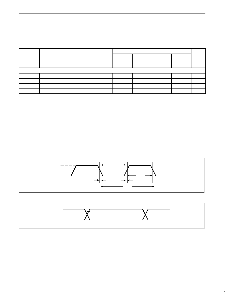
EXPLANATION OF THE AC SYMBOLS
Each timing symbol has five characters. The first character is always
`t' (= time). The other characters, depending on their positions,
indicate the name of a signal or the logical status of that signal.
The designations are:
C ≠ Clock
D ≠ Input data
H ≠ Logic level high
L ≠ Logic level low
Q ≠ Output data
T ≠ Time
V ≠ Valid
X ≠ No longer a valid logic level
Z ≠ Float
t
CHCL
t
CLCL
t
CLCH
t
CHCX
V
CC
≠0.5
0.45V
0.2 V
CC
+ 0.9
0.2 V
CC
≠ 0.1
t
CLCX
SU00297
Figure 4. External Clock Drive
0.2 V
CC
+ 0.9
0.2 V
CC
≠ 0.1
V
CC
≠0.5
0.45V
SU00307
Figure 5. AC Testing Input/Output
Philips Semiconductors
Product specification
83C752/87C752
80C51 8-bit microcontroller family
2K/64 OTP/ROM, 5 channel 8 bit A/D, I
2
C, PWM, low pin count
1998 May 01
16
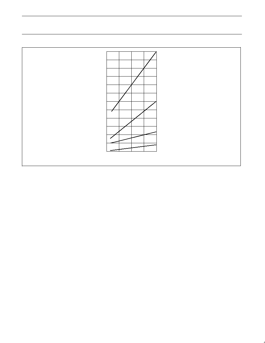
4MHz
8MHz
12MHz
16MHz
FREQ
MAX ACTIVE ICC
6
TYP ACTIVE ICC
6
MAX IDLE ICC
7
TYP IDLE ICC
7
ICC mA
2
4
6
8
10
12
14
16
18
20
22
SU00308
Figure 6. I
CC
vs. FREQ
Maximum I
CC
values taken at V
CC
= 5.5V and worst case temperature.
Typical I
CC
values taken at V
CC
= 5.0V and 25
∞
C.
Notes 6 and 7 refer to AC Electrical Characteristics.
PROGRAMMING CONSIDERATIONS
EPROM Characteristics
The 87C752 is programmed by using a modified Quick-Pulse
Programming algorithm similar to that used for devices such as the
87C451 and 87C51. It differs from these devices in that a serial data
stream is used to place the 87C752 in the programming mode.
Figure 7 shows a block diagram of the programming configuration
for the 87C752. Port pin P0.2 is used as the programming voltage
supply input (V
PP
signal). Port pin P0.1 is used as the program
(PGM/) signal. This pin is used for the 25 programming pulses.
Port 3 is used as the address input for the byte to be programmed
and accepts both the high and low components of the eleven bit
address. Multiplexing of these address components is performed
using the ASEL input. The user should drive the ASEL input high
and then drive port 3 with the high order bits of the address. ASEL
should remain high for at least 13 clock cycles. ASEL may then be
driven low which latches the high order bits of the address internally.
The high address should remain on port 3 for at least two clock
cycles after ASEL is driven low. Port 3 may then be driven with the
low byte of the address. The low address will be internally stable 13
clock cycles later. The address will remain stable provided that the
low byte placed on port 3 is held stable and ASEL is kept low. Note:
ASEL needs to be pulsed high only to change the high byte of the
address.
Port 1 is used as a bidirectional data bus during programming and
verify operations. During programming mode, it accepts the byte to
be programmed. During verify mode, it provides the contents of the
EPROM location specified by the address which has been supplied
to Port 3.
The XTAL1 pin is the oscillator input and receives the master system
clock. This clock should be between 1.2 and 6MHz.
The RESET pin is used to accept the serial data stream that places
the 87C752 into various programming modes. This pattern consists
of a 10-bit code with the LSB sent first. Each bit is synchronized to
the clock input, X1.
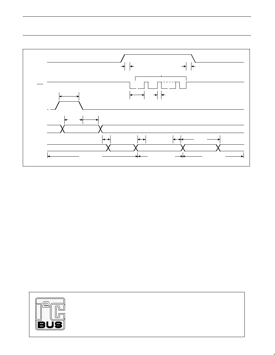
Programming Operation
Figures 8 and 9 show the timing diagrams for the program/verify
cycle. RESET should initially be held high for at least two machine
cycles. P0.1 (PGM/) and P0.2 (V
PP
) will be at V
OH
as a result of the
RESET operation. At this point, these pins function as normal
quasi-bidirectional I/O ports and the programming equipment may
pull these lines low. However, prior to sending the 10-bit code on the
RESET pin, the programming equipment should drive these pins
high (V
IH
). The RESET pin may now be used as the serial data input
for the data stream which places the 87C752 in the programming
mode. Data bits are sampled during the clock high time and thus
should only change during the time that the clock is low. Following
transmission of the last data bit, the RESET pin should be held low.
Next the address information for the location to be programmed is
placed on port 3 and ASEL is used to perform the address
multiplexing, as previously described. At this time, port 1 functions
as an output.

Philips Semiconductors
Product specification
83C752/87C752
80C51 8-bit microcontroller family
2K/64 OTP/ROM, 5 channel 8 bit A/D, I
2
C, PWM, low pin count
1998 May 01
17
A high voltage V
PP
level is then applied to the V
PP
input (P0.2).
(This sets Port 1 as an input port). The data to be programmed into
the EPROM array is then placed on Port 1. This is followed by a
series of programming pulses applied to the PGM/ pin (P0.1). These
pulses are created by driving P0.1 low and then high. This pulse is
repeated until a total of 25 programming pulses have occurred. At
the conclusion of the last pulse, the PGM/ signal should remain high.
The V
PP
signal may now be driven to the V
OH
level, placing the
87C752 in the verify mode. (Port 1 is now used as an output port).
After four machine cycles (48 clock periods), the contents of the
addressed location in the EPROM array will appear on Port 1.
The next programming cycle may now be initiated by placing the
address information at the inputs of the multiplexed buffers, driving
the V
PP
pin to the V
PP
voltage level, providing the byte to be
programmed to Port1 and issuing the 26 programming pulses on the
PGM/ pin, bringing V
PP
back down to the V
C
level and verifying the
byte.
Programming Modes
The 87C752 has four programming features incorporated within its
EPROM array. These include the USER EPROM for storage of the
application's code, a 16-byte encryption key array and two security
bits. Programming and verification of these four elements are
selected by a combination of the serial data stream applied to the
RESET pin and the voltage levels applied to port pins P0.1 and
P0.2. The various combinations are shown in Table 4.
Encryption Key Table
The 87C752 includes a 16-byte EPROM array that is programmable
by the end user. The contents of this array can then be used to
encrypt the program memory contents during a program memory
verify operation. When a program memory verify operation is
performed, the contents of the program memory location is
XNOR'ed with one of the bytes in the 16-byte encryption table. The
resulting data pattern is then provided to port 1 as the verify data.
The encryption mechanism can be disable, in essence, by leaving
the bytes in the encryption table in their erased state (FFH) since
the XNOR product of a bit with a logical one will result in the original
bit. The encryption bytes are mapped with the code memory in
16-byte groups. the first byte in code memory will be encrypted with
the first byte in the encryption table; the second byte in code
memory will be encrypted with the second byte in the encryption
table and so forth up to and including the 16the byte. The encryption
repeats in 16-byte groups; the 17th byte in the code memory will be
encrypted with the first byte in the encryption table, and so forth.
Security Bits
Two security bits, security bit 1 and security bit 2, are provided to
limit access to the USER EPROM and encryption key arrays.
Security bit 1 is the program inhibit bit, and once programmed
performs the following functions:
1. Additional programming of the USER EPROM is inhibited.
2. Additional programming of the encryption key is inhibited.
3. Verification of the encryption key is inhibited.
4. Verification of the USER EPROM and the security bit levels may
still be performed.
(If the encryption key array is being used, this security bit should be
programmed by the user to prevent unauthorized parties from
reprogramming the encryption key to all logical zero bits. Such
programming would provide data during a verify cycle that is the
logical complement of the USER EPROM contents).
Security bit 2, the verify inhibit bit, prevents verification of both the
USER EPROM array and the encryption key arrays. The security bit
levels may still be verified.
Programming and Verifying Security Bits
Security bits are programmed employing the same techniques used
to program the USER EPROM and KEY arrays using serial data
streams and logic levels on port pins indicated in Table 4. When
programming either security bit, it is not necessary to provide
address or data information to the 87C752 on ports 1 and 3.
Verification occurs in a similar manner using the RESET serial
stream shown in Table 4. Port 3 is not required to be driven and the
results of the verify operation will appear on ports 1.6 and 1.7.
Ports 1.7 contains the security bit 1 data and is a logical one if
programmed and a logical zero if not programmed. Likewise, P1.6
contains the security bit 2 data and is a logical one if programmed
and a logical zero if not programmed.
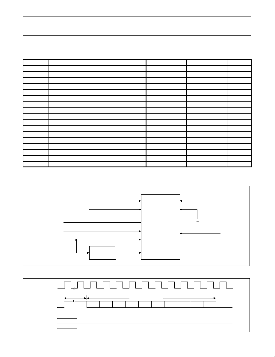
Table 4. Implementing Program/Verify Modes
OPERATION
SERIAL CODE
P0.1 (PGM/)
P0.2 (V
PP
)
Program user EPROM
296H
≠*
V
PP
Verify user EPROM
296H
V
IH
V
IH
Program key EPROM
292H
≠*
V
PP
Verify key EPROM
292H
V
IH
V
IH
Program security bit 1
29AH
≠*
V
PP
Program security bit 2
298H
≠*
V
PP
Verify security bits
29AH
V
IH
V
IH
NOTE:
*
Pulsed from V
IH
to V
IL
and returned to V
IH
.
Philips Semiconductors
Product specification
83C752/87C752
80C51 8-bit microcontroller family
2K/64 OTP/ROM, 5 channel 8 bit A/D, I
2
C, PWM, low pin count
1998 May 01
18
EPROM PROGRAMMING AND VERIFICATION
T
amb
= 21
∞
C to +27
∞
C, V
CC
= 5V
±
10%, V
SS
= 0V
SYMBOL
PARAMETER
MIN
MAX
UNIT
1/t
CLCL
Oscillator/clock frequency
1.2
6
MHz
t
AVGL
1
Address setup to P0.1 (PROG≠) low
10
µ
s + 24t
CLCL
t
GHAX
Address hold after P0.1 (PROG≠) high
48t
CLCL
t
DVGL
Data setup to P0.1 (PROG≠) low
38t
CLCL
t
DVGL
Data setup to P0.1 (PROG≠) low
38t
CLCL
t
GHDX
Data hold after P0.1 (PROG≠) high
36t
CLCL
t
SHGL
V
PP
setup to P0.1 (PROG≠) low
10
µ
s
t
GHSL
V
PP
hold after P0.1 (PROG≠)
10
µ
s
t
GLGH
P0.1 (PROG≠) width
90
110
µ
s
t
AVQV
2
V
PP
low (V
CC
) to data valid
48t
CLCL
t
GHGL
P0.1 (PROG≠) high to P0.1 (PROG≠) low
10
µ
s
t
SYNL
P0.0 (sync pulse) low
4t
CLCL
t
SYNH
P0.0 (sync pulse) high
8t
CLCL
t
MASEL
ASEL high time
13t
CLCL
t
MAHLD
Address hold time
2t
CLCL
t
HASET
Address setup to ASEL
13t
CLCL
t
ADSTA
Low address to address stable
13t
CLCL
NOTES:
1. Address should be valid at least 24t
CLCL
before the rising edge of P0.2 (V
PP
).
2. For a pure verify mode, i.e., no program mode in between, t
AVQV
is 14t
CLCL
maximum.
A0≠A10
ADDRESS STROBE
PROGRAMMING
PULSES
VPP/VIH VOLTAGE
SOURCE
CLK SOURCE
RESET
CONTROL
LOGIC
87C752
P3.0≠P3.7
P0.0/ASEL
P0.1
P0.2
XTAL1
RESET
V
CC
V
SS
P1.0≠P1.7
+5V
DATA BUS
SU00320
Figure 7. Programming Configuration
MIN 2 MACHINE
CYCLES
TEN BIT SERIAL CODE
BIT 0
BIT 1
BIT 2
BIT 3
BIT 4
BIT 5
BIT 6
BIT 7
BIT 8
BIT 9
UNDEFINED
UNDEFINED
XTAL1
RESET
P0.2
P0.1
SU00302
Figure 8. Entry into Program/Verify Modes
Philips Semiconductors
Product specification
83C752/87C752
80C51 8-bit microcontroller family
2K/64 OTP/ROM, 5 channel 8 bit A/D, I
2
C, PWM, low pin count
1998 May 01
19
5V
12.75V
5V
25 PULSES
tSHGL
tGHSL
tGLGH
tGHGL
98
µ
s MIN
10
µ
s MIN
tMASEL
tHASET
tHAHLD
tADSTA
tDVGL
tGHDX
tAVQV
VERIFY MODE
PROGRAM MODE
VERIFY MODE
P0.2 (VPP)
P0.1 (PGM)
P0.0 (ASEL)
PORT 3
PORT 1
INVALID DATA
VALID DATA
DATA TO BE PROGRAMMED
INVALID DATA
VALID DATA
HIGH ADDRESS
LOW ADDRESS
SU00310
Figure 9. Program/Verify Cycle
Purchase of Philips I
2
C components conveys a license under the Philips' I
2
C patent
to use the components in the I
2
C system provided the system conforms to the
I
2
C specifications defined by Philips. This specification can be ordered using the
code 9398 393 40011.
Philips Semiconductors
Product specification
83C752/87C752
80C51 8-bit microcontroller family
2K/64 OTP/ROM, 5 channel 8 bit A/D, I
2
C, PWM, low pin count
1998 May 01
20
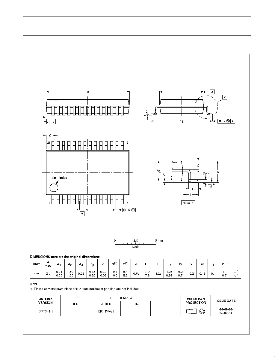
SSOP28:
plastic shrink small outline package; 28 leads; body width 5.3mm
SOT341-1
Philips Semiconductors
Product specification
83C752/87C752
80C51 8-bit microcontroller family
2K/64 OTP/ROM, 5 channel 8 bit A/D, I
2
C, PWM, low pin count
1998 May 01
21
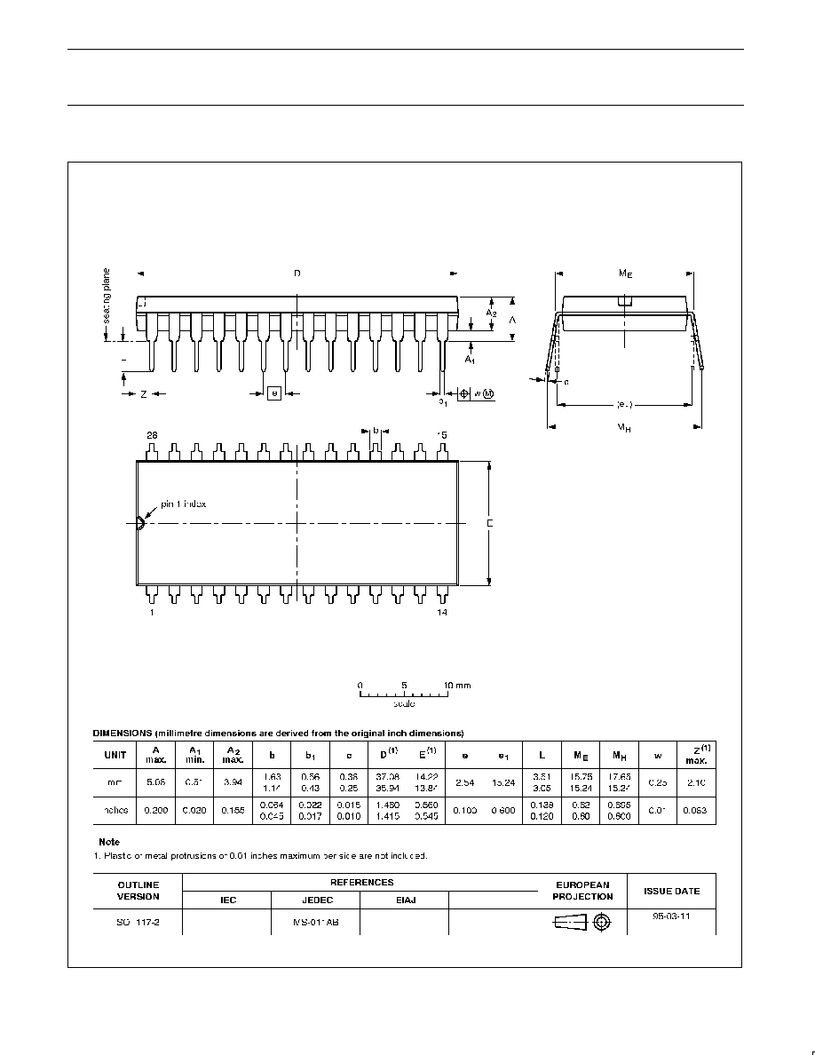
DIP28:
plastic dual in-line package; 28 leads (600 mil); long body
SOT117-2
Philips Semiconductors
Product specification
83C752/87C752
80C51 8-bit microcontroller family
2K/64 OTP/ROM, 5 channel 8 bit A/D, I
2
C, PWM, low pin count
1998 May 01
22
PLCC28:
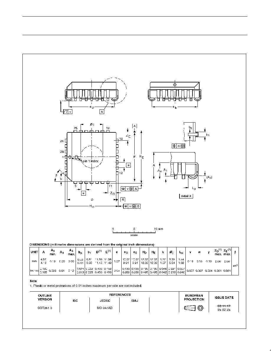
plastic leaded chip carrer; 28 leads; pedestal
SOT261-3

Philips Semiconductors
Product specification
83C752/87C752
80C51 8-bit microcontroller family
2K/64 OTP/ROM, 5 channel 8 bit A/D, I
2
C, PWM, low pin count
1998 May 01
23
NOTES

Philips Semiconductors
Product specification
83C752/87C752
80C51 8-bit microcontroller family
2K/64 OTP/ROM, 5 channel 8 bit A/D, I
2
C, PWM, low pin count
1998 May 01
24
Definitions
Short-form specification -- The data in a short-form specification is extracted from a full data sheet with the same type number and title. For
detailed information see the relevant data sheet or data handbook.
Limiting values definition -- Limiting values given are in accordance with the Absolute Maximum Rating System (IEC 134). Stress above one
or more of the limiting values may cause permanent damage to the device. These are stress ratings only and operation of the device at these or
at any other conditions above those given in the Characteristics sections of the specification is not implied. Exposure to limiting values for extended
periods may affect device reliability.
Application information -- Applications that are described herein for any of these products are for illustrative purposes only. Philips
Semiconductors make no representation or warranty that such applications will be suitable for the specified use without further testing or
modification.
Disclaimers
Life support -- These products are not designed for use in life support appliances, devices or systems where malfunction of these products can
reasonably be expected to result in personal injury. Philips Semiconductors customers using or selling these products for use in such applications
do so at their own risk and agree to fully indemnify Philips Semiconductors for any damages resulting from such application.
Right to make changes -- Philips Semiconductors reserves the right to make changes, without notice, in the products, including circuits, standard
cells, and/or software, described or contained herein in order to improve design and/or performance. Philips Semiconductors assumes no
responsibility or liability for the use of any of these products, conveys no license or title under any patent, copyright, or mask work right to these
products, and makes no representations or warranties that these products are free from patent, copyright, or mask work right infringement, unless
otherwise specified.
Philips Semiconductors
811 East Arques Avenue
P.O. Box 3409
Sunnyvale, California 94088≠3409
Telephone 800-234-7381
©
Copyright Philips Electronics North America Corporation 1998
All rights reserved. Printed in U.S.A.
Date of release: 05-98
Document order number:
9397 750 03843
Philips
Semiconductors
Data sheet
status
Objective
specification
Preliminary
specification
Product
specification
Product
status
Development
Qualification
Production
Definition
[1]
This data sheet contains the design target or goal specifications for product development.
Specification may change in any manner without notice.
This data sheet contains preliminary data, and supplementary data will be published at a later date.
Philips Semiconductors reserves the right to make chages at any time without notice in order to
improve design and supply the best possible product.
This data sheet contains final specifications. Philips Semiconductors reserves the right to make
changes at any time without notice in order to improve design and supply the best possible product.
Data sheet status
[1]
Please consult the most recently issued datasheet before initiating or completing a design.