
ABT22V10A5, A7
5V high-speed universal PLD device
with live insertion capability
Product specification
1996 Dec 16
INTEGRATED CIRCUITS
IC13 Data Handbook

Philips Semiconductors
Product specification
ABT22V10A5, A7
5V high-speed universal PLD device
with live insertion capability
2
1996 Dec 16
853≠1795 17606
DESCRIPTION
The ABT22V10A is a versatile PAL
Æ
device fabricated on Philips
BiCMOS process known as QUBiC.
The QUBiC process produces very high speed, 5 volt devices
(5.0ns) which have excellent noise immunity. The ground bounce of
an output held low while the 9 remaining outputs are switching is
less than 1.0V (typical).
The ABT22V10A outputs are designed to support Live
Insertion/Extraction into powered-up systems. The output is
specially designed so that during V
CC
ramp, the output remains
3-Stated until V
CC
2.1V. At that time, the outputs become fully
functional, depending upon device inputs. (See DC Electrical
Characteristics, Symbol I
PU/PD
, Page 4).
The ABT family of devices have virtually no ground bounce-- less
than 1.0 volts V
OLP
, measured on an unswitched output (9 remaining
outputs switching, each with a 50pF load tied to ground).
The ABT family of devices has been designed with high drive
outputs (48mA sink and 16mA source currents), which allow for
direct connection to a backplane bus. This feature eliminates the
need for additional, standalone bus drivers, which are traditionally
required to boost the drive of a standard 16/≠4mA PLDs.
Philips has developed a new means of testing the integrity of fuses,
both blown and intact fuses, which insures that all the fuses have
been correctly programmed and that each and every fuse--whether
"blown" or "intact"--is at the appropriate and optimal fuse resistance.
This dual verify scheme represents a significant improvement over
single reference voltage comparison schemes that have been used
for bipolar devices since the late 1980's.
The ABT22V10A uses the familiar AND/OR logic array structure,
which allows direct implementation of sum-of-products equations.
This device has a programmable AND array, which drives a fixed
OR array. The OR sum-of-products feeds an "Output Macro Cell"
(OMC) that can be individually configured as a dedicated input, a
combinatorial output, or a registered output with internal feedback.
FEATURES
∑
Fastest 5V 22V10
∑
Low ground bounce (<1.0V typical)
∑
Live insertion/extraction permitted
∑
High output drive capability: 48mA/≠16mA
∑
Varied product term distribution with up to 16 product terms per
output for complex functions
∑
Metastable hardened flip-flops
∑
Programmable output polarity
∑
Design support provided for third party CAD development and
programming hardware
∑
Improved fuse verification circuitry increases reliability
PIN CONFIGURATIONS
VCC
1
2
3
4
5
6
7
8
9
10
11
12
13
14
15
16
17
18
19
20
21
22
23
24
25
26
27
28
GND
A Package
GND
I7
CLK/
I0
I1
I2
I3
I4
I5
GND
I6
I8
I9
I10 GND
I11
F0
F1
F2
F3
F7
F6
F5
F4
F8
F9
A = Plastic Leaded Chip Carrier
VCC
SP00367
PIN LABEL DESCRIPTIONS
SYMBOL
FUNCTION
I1 ≠ I11
Dedicated Input
F0 ≠ F9
Macro Cell Input/Output
CLK/I0
Clock Input/Dedicated Input
V
CC
Supply Voltage
GND
Ground
ORDERING INFORMATION
DESCRIPTION
ORDER CODE
DRAWING NUMBER
28-Pin Plastic Leaded Chip Carrier
ABT22V10A5A
(5ns device)
SOT261-3
28-Pin Plastic Leaded Chip Carrier
ABT22V10A7A
(7.5ns device)
SOT261-3
©
PAL is a registered trademark of Advanced Micro Devices, Inc.

Philips Semiconductors
Product specification
ABT22V10A5, A7
5V high-speed universal PLD device
with live insertion capability
1996 Dec 16
3
ABSOLUTE MAXIMUM RATINGS
1
SYMBOL
PARAMETER
RATINGS
UNIT
SYMBOL
PARAMETER
MIN
MAX
UNIT
V
CC
Supply voltage
2
≠0.5
+7.0
V
DC
V
IN
Input voltage
2
≠1.2
V
CC
+ 0.5
V
DC
V
OUT
Output voltage
≠0.5
V
CC
+ 0.5
V
DC
I
IN
Input currents
≠30
+30
mA
I
OUT
Output currents
+100
mA
T
stg
Storage temperature range
≠65
+150
∞
C
NOTES:
1. Stresses above those listed may cause malfunction or permanent damage to the device. This is a stress rating only. Functional operation at
these or any other condition above those indicated in the operational and programming specification of the device is not implied.
2. Except in programming mode.
OPERATING RANGES
SYMBOL
PARAMETER
RATINGS
UNIT
SYMBOL
PARAMETER
MIN
MAX
UNIT
V
CC
Supply voltage
+4.75
+5.25
V
DC
T
amb
Operating free-air temperature
0
+75
∞
C
THERMAL RATINGS
TEMPERATURE
Maximum junction
150
∞
C
Maximum ambient
75
∞
C
Allowable thermal rise ambient to junction
75
∞
C
VOLTAGE WAVEFORM
90%
10%
1.5ns
1.5ns
+3.0V
0V
t
R
t
F
MEASUREMENTS:
All circuit delays are measured at the +1.5V level of
inputs and outputs, unless otherwise specified.
Input Pulses
SP00368
TEST LOAD CIRCUIT
+5V
C
L
R
1
R
2
S
1
C
2
C
1
NOTE:
C
1
and C
2
are to bypass V
CC
to GND.
V
CC
GND
CK
I
n
I
0
F
0
F
n
DUT
OE
INPUTS
SP00369
Philips Semiconductors
Product specification
ABT22V10A5, A7
5V high-speed universal PLD device
with live insertion capability
1996 Dec 16
4
DC ELECTRICAL CHARACTERISTICS
Over operating ranges.
SYMBOL
PARAMETER
TEST CONDITIONS
1
LIMITS
UNIT
SYMBOL
PARAMETER
TEST CONDITIONS
1
MIN
MAX
UNIT
Input voltage
V
IL
Low
V
CC
= MIN
0.8
V
V
IH
High
V
CC
= MAX
2.0
V
V
I
Clamp
V
CC
= MIN, I
IN
= ≠18mA
≠1.2
V
Output voltage
V
OH
High-level output voltage
V
CC
= MIN
V
I
= V
IH
or V
IL
I
OH
= ≠32mA
2.0
V
V
OH
High-level output voltage
V
CC
= MIN
V
I
= V
IH
or V
IL
I
OH
= ≠16mA
2.4
V
V
OL
Low-level output voltage
V
CC
= MIN
V
I
= V
IH
or V
IL
I
OL
= 48mA
0.5
V
Input current
I
IL
Low
V
CC
= MAX, V
IN
= 0.4V
≠10
µ
A
I
IH
High
V
CC
= MAX, V
IN
= 2.7V
10
µ
A
I
I
Max input current
V
CC
= MAX, V
IN
= 5.5V
20
µ
A
Output current
I
PU/PD
Power-up/down 3-State
output current
4
V
CC
<2.1V; V
O
= 0.5V to V
CC
;
V
I
= GND or V
CC
; OE/OE = X
50
µ
A
V
CC
= MAX
I
OZH
Output leakage
2
V
IN
= V
IL
or V
IH
, V
OUT
= 2.7V
20
µ
A
I
OZL
Output leakage
2
V
IN
= V
IL
or V
IH
, V
OUT
=0.4V
≠20
µ
A
I
SC
Short circuit
3
V
OUT
= 0.5V
≠30
≠220
mA
I
CC
V
CC
supply current
V
CC
= MAX, Outputs enabled, V
I
= V
CC
or GND; I
O
= 0
200
mA
Ground Bounce
TYP
MAX
UNIT
V
OLP
Minimum dynamic V
OH
5
V
CC
= MAX, 25
∞
C
C
L
= 50pF (including jig capacitance)
1.0
1.2
V
NOTES:
1. These are absolute values with respect to device ground and all overshoots due to system or tester noise are included.
2. I/O pin leakage is the worst case of I
OZX
or I
IX
(where X = H or L).
3. No more than one output should be tested at a time. Duration of the short-circuit test should not exceed one second. V
OUT
= 0.5V has been
chosen to avoid test problems caused by tester ground degradation.
4. This parameter is valid for any V
CC
between 0V and 1.2 V with a transition time up to 10 mS. From V
CC
= 1.2 to V
CC
= 5.0V
±
0.25V a
transition time of 100
µ
S is permitted. X = Don't care.
5. Guaranteed by design, but not tested. Measured holding one output (the output under test) Low and simultaneously switching all remianing
output from a High to a Low state. Switch S1 is closed; 50pF load.
Philips Semiconductors
Product specification
ABT22V10A5, A7
5V high-speed universal PLD device
with live insertion capability
1996 Dec 16
5
AC ELECTRICAL CHARACTERISTICS
1
4.75V
V
CC
5.25V; 0
_
C
T
amb
+75
_
C
SYMBOL
PARAMETER
TEST
CONDITIONS
LIMITS
UNIT
SYMBOL
PARAMETER
TEST
CONDITIONS
ABT22V10A5
ABT22V10A7
UNIT
CONDITIONS
MIN
TYP
MAX
MIN
TYP
MAX
t
PD
Input or feedback to
non-registered output
2
Active-LOW
2.0
4.5
5.0
2.0
6.0
7.5
ns
t
PD
Input or feedback to
non-registered output
2
Active-HIGH
2.0
4.5
5.0
2.0
6.0
7.5
ns
t
S
Setup time from input or SP
to Clock
2.0
1.3
3.5
3.0
ns
t
SIO
Setup time from feedback
to Clock
2.25
1.5
3.5
3.0
ns
t
H
Hold time
0
0
ns
t
SKEWR
Skew between registered
outputs
4, 7
1.0
1.0
ns
t
CO
Clock to output
2.0
3.5
4.0
2.0
4.5
5.5
ns
t
CF
Clock to feedback
3
2.0
4.0
3.0
5.0
ns
t
AR
Asynchronous Reset to
registered output
10.0
10.0
ns
t
ARW
Asynchronous Reset width
6.0
7.5
ns
t
ARR
Asynchronous Reset
recovery time
4.0
5.5
ns
t
SPR
Synchronous Preset
recovery time
4.5
5.0
ns
t
WL
Width of Clock LOW
2.0
3.0
ns
t
WH
Width of Clock HIGH
2.0
3.0
ns
f
MAX
Maximum frequency;
External feedback
1/(t
S
+ t
CO
)
4
167
208
111
133
MHz
f
MAX
Maximum frequency;
Internal feedback
1/(t
S
+ t
CF
)
4
167
303
125
166
MHz
t
EA
Input to Output Enable
5
8.0
8.0
ns
t
ER
Input to Output Disable
5
7.5
7.5
ns
Capacitance
6
C
IN
Input Capacitance (Pin 2)
V
IN
= 2.0V
V
CC
= 5.0V
T
amb
= 25
∞
C
f = 1MHz
8
8
pF
C
IN
Input Capacitance (Others)
V
IN
= 2.0V
V
CC
= 5.0V
T
amb
= 25
∞
C
f = 1MHz
4
4
pF
C
OUT
Output Capacitance
V
OUT
= 2.0V
f = 1MHz
8
8
pF
NOTES:
1. Test Conditions: R
1
= 300
, R
2
=390
2. t
PD
is tested with switch S
1
closed and C
L
= 50pF (including jig capacitance). V
IH
= 3V, V
IL
= 0V, V
T
= 1.5V.
3. Calculated from measured f
MAX
internal.
4. These parameters are not 100% tested, but are calculated at initial characterization and at any time the design is modified where frequency
may be affected.
5. For 3-State output; output enable times are tested with C
L
= 50pF to the 1.5V level, and S
1
is open for high-impedance to High tests and
closed for high-impedance to Low tests. Output disable times are tested with C
L =
5pF. High-to-High impedance tests are made to an output
voltage of V
T
= (V
OH
≠ 0.5V) with S
1
open, and Low-to-High impedance tests are made to the V
T
= (V
OL
+ 0.5V) level with S
1
closed.
6. These parameters are not 100% tested, but are evaluated at initial characterization and at any time the design is modified where
capacitance may be affected.
7. Skew is measured with all outputs switching in the same direction.

Philips Semiconductors
Product specification
ABT22V10A5, A7
5V high-speed universal PLD device
with live insertion capability
1996 Dec 16
6
PRODUCT FEATURES
Low Ground Bounce
The Philips Semiconductors BiCMOS QUBiC process produces
exceptional noise immunity. The typical ground bounce, with 9
outputs simultaneously switching and the 10th output held low, is
less than 1.0V. V
OLP
is tested by holding one output (the output
uncer test) in the Low state and then simultaneously switching all
remaining outputs from a High to a Low state (each output is loaded
with 50pF). The maximum peak voltage on the output under test is
guaranteed to be less than 1.2 Volts.
Live Insertion/Extraction Capability
There are some inherent problems associated with inserting or
extracting an unpowered module from a powered-up, active system.
The ABT22V10A outputs have been designed such that any chance
of bus contention, glitching or clamping is eliminated.
Detailed information on this feature is provided in an application note
AN051:
Philips PLDs Support Live Insertion Applications.
Improved Fuse Verification Circuitry Increases
Reliability
Philips has developed a new means of testing the integrity of fuses,
both blown and intact fuses, which insures that all the fuses have
been correctly programmed and that each and every fuse ≠ whether
"blown" or "intact" ≠ is at the appropriate and optimal fuse
resistance. This dual verify scheme represents a significant
improvement over single reference voltage comparisons schemes
that have been used for bipolar devices since the late 1980s.
Detailed information on this feature is provided in an application note
entitled
Dual Verify Technique Increases Reliability of PLDs.
Programmable 3-stage Outputs
Each output has a 3-Stage output buffer with 3-State control. A
product term controls the buffer, allowing enable and disable to be a
function of any product of device inputs or output feedback. The
combinatorial output provides a bidirectional I/O pin, and may be
configured as a dedicated input if the buffer is always disabled.
Programmable Output Polarity
The polarity of each macro cell output can be Active-HIGH or
Active-LOW, either to match output signal needs or to reduce
product terms. Programmable polarity allows Boolean expressions
to be written in their most compact form (true or inverted), and the
output can still be of the desired polarity. It can also save
"DeMorganizing" efforts.
Selection is controlled by programmable bit S
0
in the Output Macro
Cell, and affects both registered and combinatorial outputs.
Selection is automatic, based on the design specification and pin
definitions. If the pin definition and output equation have the same
polarity, the output is programmed to be Active-HIGH (S
0
= 1).
Preset/Reset
For initialization, the ABT22V10A has additional Preset and Reset
product terms. These terms are connected to all registered outputs.
When the Synchronous Preset (SP) product term is asserted high,
the output registers will be loaded with a HIGH on the next
LOW-to-HIGH clock transition. When the Asynchronous Reset (AR)
product term is asserted high, the output registers will be
immediately loaded with a LOW, independent of the clock.
Note that Preset and Reset control the flip-flop, not the output pin.
The output level is determined by the output polarity selected.
Power-Up Reset
All flip-flops power-up to a logic LOW for predictable system
initialization. Outputs of the ABT22V10A will depend on the
programmed output polarity. The V
CC
rise must be monotonic and
the reset delay time is 1≠10
µ
s maximum.
Security Fuse
After programming and verification, ABT22V10A designs can be
secured by programming the security fuse link. Once programmed,
this fuse defeats readback of the internal programmed pattern by a
device programmer, securing proprietary designs from competitors.
When the security fuse is programmed, the array will read as if
every fuse is programmed.
Quality and Testability
The ABT22V10A offers a very high level of built-in quality. Extra
programmable fuses provide a means of verifying performance of all
AC and DC parameters. In addition, this verifies programmability
and functionality of the device to provide the highest programming
and post-programming functional yields.
Technology
The BiCMOS ABT22V10A is fabricated with the Philips
Semiconductors process known as QUBiC. QUBiC combines an
advanced, state-of-the-art 1.0
µ
m (drawn feature size) CMOS
process with an ultra fast bipolar process to achieve superior speed
and drive capabilities. QUBiC incorporates three layers of Al/Cu
interconnects for reduced chip size, and our proven Ti-W fuse
technology ensures highest programming yields.
Programming
The ABT22V10A is fully supported by industry standard (JEDEC
compatible) PLD CAD tools, including Philips Semiconductors
SNAP design software package. ABEL
TM
CUPL
TM
and PALASM
Æ
90
design software packages also support the ABT22V10A
architecture.
All packages allow Boolean and state equation entry formats, SNAP,
ABEL and CUPL also accept, as input, schematic capture format.
Output Register Preload
The register on the ABT22V10A can be preloaded from the output
pins to facilitate functional testing of complex state machine designs.
This feature allows direct loading of arbitrary states, making it
unnecessary to cycle through long test vector sequences to reach a
desired state. In addition, transitions from illegal states can be
verified by loading illegal states and observing proper recovery. The
procedure for preloading follows:
1. Raise V
CC
to 5.0V
±
0.25V.
2. Set pin 2 or 3 to V
HH
to disable outputs and enable preload.
3. Apply the desired value (V
ILP
/V
IHP
) to all registered output pins.
Leave combinatorial output pins floating.
4. Clock Pin 1 from V
ILP
to V
IHP
.
5. Remove V
ILP
/V
IHP
from all registered output pins.
6. Lower pin 2 or 3 to V
ILP
.
7. Enable the output registers according to the programmed
pattern.
8. Verify V
OL
/V
OH
at all registered output pins. Note that the output
pin signal will depend on the output polarity.
ABEL is a trademark of Data I/O Corp.
CUPL is a trademark of Logical Devices, Inc.
PALASM is a registered trademark of AMD Corp.

Philips Semiconductors
Product specification
ABT22V10A5, A7
5V high-speed universal PLD device
with live insertion capability
1996 Dec 16
7
Metastable Characteristics
Philips provides complete data on the ABT22V10A5's metastable
characteristics. While the ABT22V10A5 does not employ Philips
patented metastable immune flip-flop, its metastabel characteristics
are still quite favorable relative to competitive devices. For
information on metastable immune PLDs, refer to the datasheets for
the ABT22V10-7 for 5V applications or the LVT22V10-7 for 3.3V
designs.
Design Example
Suppose a designer wants to use the ABT22V10A5 for
synchronizing asynchronous data that is arriving at 10MHz (as
measured by a frequency counter), in a 5V system that has a clock
frequency of 50MHz, at an ambient temperature of 25
∞
C. The next
device in the sytem samples the output fo the ABT22V10A5 5.5ns
after the clock edge to ensure that any metastable conditions that
occur have time to resolve to the correct state. The MTBF for this
situatio can be calcuclated by using the equation below:
MTBF = e(t /
)/T
0
F
C
F
1
In this formula, F
C
is the frequency of the clock, F
1
is the average
input event frequency, and t is the time after the clock pulse that the
output is sampled (t > T
CO
). T
0
and
are device parameters
provided by the semiconductor manufacturer (refer to Table 1 for the
ABT22V10A5 metastability specifications). T
0
and
are derived
from tests and can be most nearly be defined as follows:
is a
function of the rate at which a latch in a metastable state resolves
that condition. T
0
is a function of the measurement of the propensity
of a latch to enter a metastable state. T
0
is also a normalization
constant which is a very strong function of the normal propagation
dely of the device.
In this situation, the F
1
will be twice that data frequency, or 20MHz,
because input events consist of both low and high transitions. Thus
in this case F
C
is 50MHz, F
1
is 20MHz,
is 85.6ps, t is 5.5ns, and
T
0
is 4.55 seconds. Using the above formula, the actual MTBF for
this situation is 1.76
◊
10
12
seconds, or 55,889 years for the
ABT22V10A5.
Table 1. Typical Values for
and T
0
at various V
CC
's and Temperatures
V
CC
0
∞
C
+25
∞
C
+75
∞
C
V
CC
T
0
T
0
T
0
5.25V
72.00ps
7.20E+01
96.70ps
4.59E≠01
105.00ps
1.43E≠01
5.00V
72.80ps
2.06E+02
85.60ps
4.55E+00
100.00ps
8.37E≠01
4.75V
68.70ps
9.97E+03
81.70ps
4.85E+01
99.80ps
1.29E+00

Philips Semiconductors
Product specification
ABT22V10A5, A7
5V high-speed universal PLD device
with live insertion capability
1996 Dec 16
8
LOGIC DIAGRAM
NOTE:
Programmable connection.
1
1
0
0
0
1
0
1
DAR
Q
Q
SP
0
1
Q
1
1
0
0
0
1
0
1
DAR
Q
SP
0
1
Q
1
1
0
0
0
1
0
1
DAR
Q
SP
0
1
Q
1
1
0
0
0
1
0
1
DAR
Q
SP
0
1
Q
1
1
0
0
0
1
0
1
DAR
Q
SP
0
1
Q
1
1
0
0
0
1
0
1
DAR
Q
SP
0
1
Q
1
1
0
0
0
1
0
1
DAR
Q
SP
0
1
Q
1
1
0
0
0
1
0
1
DAR
Q
SP
0
1
Q
1
1
0
0
0
1
0
1
DAR
Q
SP
0
1
Q
1
1
0
0
0
1
0
1
DAR
Q
SP
0
1
AR
SP
0
3
4
7
8
11 12
15 16
19 20
23 24
27 28
31 32
35 36
39 40
43
0
3
4
7
8
11 12
15 16
19 20
23 24
27 28
31 32
35 36
39 40
43
2
3
4
5
6
7
9
10
11
12
13
14, 15, 8, 22
1, 28
27
26
25
24
23
21
20
19
18
17
16
CLK/I0
I1
I2
I3
I4
I5
I6
I7
I10
I8
I9
GND
I11
F0
F1
F2
F3
F4
F5
F6
F7
F8
F9
VCC
0
1
9
10
20
21
33
34
48
49
65
66
82
83
97
98
110
111
121
122
130
131
SP00390

Philips Semiconductors
Product specification
ABT22V10A5, A7
5V high-speed universal PLD device
with live insertion capability
1996 Dec 16
9
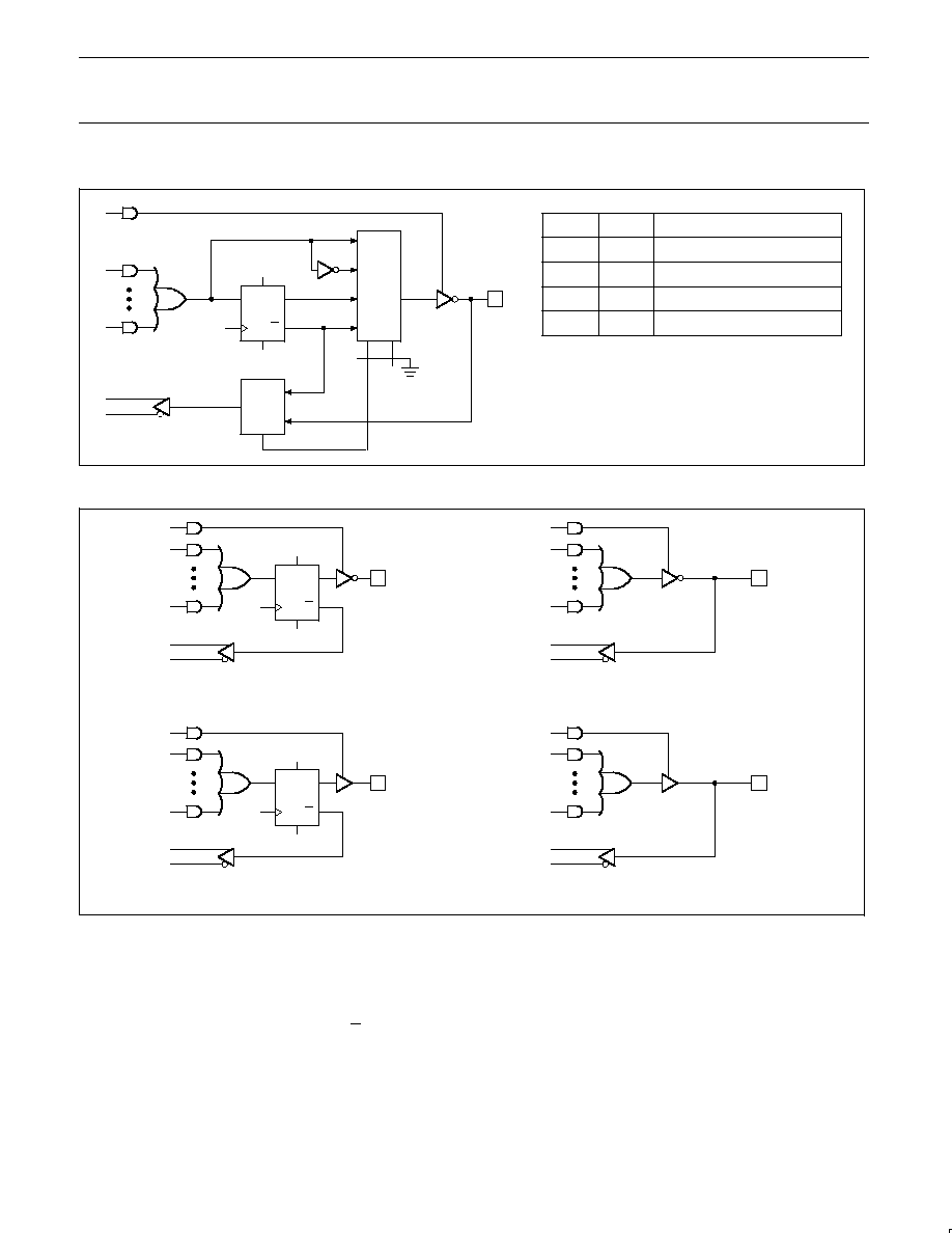
FUNCTIONAL DIAGRAM
OUTPUT
MACRO
CELL
CLK/I0
I1 ≠ I11
RESET
PRESET
F0
F1
F2
F3
F4
F5
F6
F7
F8
F9
PROGRAMMABLE AND ARRAY
(44
◊
132)
1
11
8
10
12
14
16
16
14
12
10
8
SP00060
OUTPUT
MACRO
CELL
OUTPUT
MACRO
CELL
OUTPUT
MACRO
CELL
OUTPUT
MACRO
CELL
OUTPUT
MACRO
CELL
OUTPUT
MACRO
CELL
OUTPUT
MACRO
CELL
OUTPUT
MACRO
CELL
OUTPUT
MACRO
CELL
Figure 1. Functional Diagram
FUNCTIONAL DESCRIPTION
The ABT22V10A allows the systems engineer to implement the
design on-chip, by opening fuse links to configure AND and OR
gates within the device, according to the desired logic function.
Product terms with all fuses opened assume the logical HIGH state;
product terms connected to both True and Complement of any
single input assume the logical LOW state.
The ABT22V10A has 12 inputs and 10 I/O Macro Cells (Figure 1).
The Macro Cell allows one of four potential output configurations,
registered output or combinatorial I/O, Active-HIGH or Active-LOW
(see Figure 2). The configuration choice is made according to the
user's design specification and corresponding programming of the
configuration bits S
0
≠S
1
. Multiplexer controls are connected to
ground (0) through a programmable fuse link, selecting the "0" path
through the multiplexer. Programming the fuse disconnects the
control line from GND and it floats to V
CC
(1), selecting the "1" path.
Philips Semiconductors
Product specification
ABT22V10A5, A7
5V high-speed universal PLD device
with live insertion capability
1996 Dec 16
10
OUTPUT MACRO CELL
F
0
1
1
0
0
1
0
0
1
CLK
1
AR
SP
S1
S0
S
1
S
0
OUTPUT CONFIGURATION
0 = Unprogrammed fuse
1 = Programmed fuse
D
Q
Q
0
0
1
1
0
1
0
1
Registered/Active-LOW
Registered/Active-HIGH
Combinatorial/Active-LOW
Combinatorial/Active-HIGH
SP00375
Figure 2. Output Macro Cell Logic Diagram
F
CLK
AR
SP
S0 = 0
S1 = 0
D
Q
Q
a. Registered/Active-LOW
F
CLK
AR
SP
S0 = 1
S1 = 0
D
Q
Q
b. Registered/Active-HIGH
F
S0 = 0
S1 = 1
c. Combinatorial/Active-LOW
d. Combinatorial/Active-HIGH
F
S0 = 1
S1 = 1
SP00376
Figure 3. Output Macro Cell Configurations
Registered Output Configuration
Each Macro Cell of the ABT22V10A includes a D-type flip-flop for
data storage and synchronization. The flip-flop is loaded on the
LOW-to-HIGH transition of the clock input. In the registered
configuration (S
1
= 0), the array feedback is from Q of the flip-flop.
Combinatorial I/O Configuration
Any Macro Cell can be configured as combinatorial by selecting the
multiplexer path that bypasses the flip-flop (S
1
= 1). In the
combinatorial configuration, the feedback is from the pin.
Variable Input/Output Pin Ratio
The ABT22V10A has twelve dedicated input lines, and each Macro
Cell output can be an I/O pin. Buffers for device inputs have
complementary outputs to provide user-programmable input signal
polarity.
Philips Semiconductors
Product specification
ABT22V10A5, A7
5V high-speed universal PLD device
with live insertion capability
1996 Dec 16
11
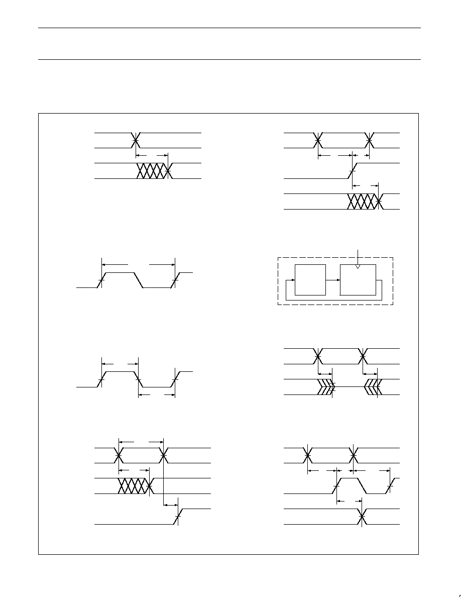
SWITCHING WAVEFORMS
V
T
= 1.5V.
Input pulse amplitude 0V to 3.0V.
Input rise and fall times 1.5ns max.
tS
Combinatorial Output
Registered Output
Clock to Feedback (f
MAX
Internal)
(See Path at Right)
Clock Width
Input to Output Disable/Enable
Asynchronous Reset
Synchronous Preset
tPD
VT
VT
INPUT OR
FEEDBACK
COMBINATORIAL
OUTPUT
VT
VT
VT
INPUT OR
FEEDBACK
CLOCK
REGISTERED
OUTPUT
tS
tH
tCO
VT
tS + tCF
CLOCK
LOGIC
REGISTER
CLK
tS
tCF
VT
tWH
CLOCK
tWL
tER
tEA
VOH ≠ 0.5V
VOL + 0.5V
INPUT
OUTPUT
VT
VT
VT
VT
VT
tARW
tAR
tARR
CLOCK
REGISTERED
OUTPUT
INPUT ASSERTING
ASYNCHRONOUS
RESET
tH
VT
VT
VT
VT
tSPR
INPUT ASSERTING
SYNCHRONOUS
PRESET
CLOCK
REGISTERED
OUTPUT
tCO
SP00377
Clock to Feedback

Philips Semiconductors
Product specification
ABT22V10A5, A7
5V high-speed universal PLD device
with live insertion capability
1996 Dec 16
12
"AND" ARRAY ≠ (I, B)
I, B
P, D
CODE
O
STATE
INACTIVE1
CODE
STATE
CODE
STATE
CODE
STATE
TRUE
H
L
--
P, D
I, B
I, B
P, D
I, B
I, B
P, D
I, B
I, B
I, B
COMPLEMENT
DON'T CARE
SP00008
I, B
I, B
I, B
I, B
NOTE:
1. This is the initial state.
PRELOAD SET-UP
SYMBOL
PARAMETER
LIMITS
UNIT
SYMBOL
PARAMETER
MIN
REC
MAX
UNIT
V
HH
Super-level input voltage
9.5
9.5
10
V
V
ILH
Low-level input voltage
0
0
0.8
V
V
IHP
High-level input voltage
2.4
5.0
5.5
V
t
D
Delay time
100
200
1000
ns
t
I/O
I/O valid after Pin 2 or 3 drops from V
HH
to V
ILP
100
ns
t
D
V
HH
V
IHP
V
OH
V
OL
V
ILP
V
IHP
V
ILP
t
I/O
PINS 2, 3
REGISTERED
OUTPUTS
CLOCK
t
D
t
D
t
D
t
D
Output Register Preload Waveform
DATA IN
DATA OUT
V
ILP
SP00373

Philips Semiconductors
Product specification
ABT22V10A5, A7
5V high-speed universal PLD device
with live insertion capability
1996 Dec 16
13
POWER-UP RESET
The power-up reset feature ensures that all flip-flops will be reset to
LOW after the device has been powered up. The output state will
depend on the programmed pattern. This feature is valuable in
simplifying state machine initialization. A timing diagram and
parameter table are shown below. Due to the synchronous operation
of the power-up reset and the wide range of ways V
CC
can rise to its
steady state, two conditions are required to ensure a valid power-up
reset. These conditions are:
1. The V
CC
rise must be monotonic.
2. Following reset, the clock input must not be driven from LOW to
HIGH until all applicable input and feedback setup times are met.
SYMBOL
PARAMETER
LIMITS
UNIT
SYMBOL
PARAMETER
MIN
MAX
UNIT
t
PR
Power-up Reset Time
1
µ
s
t
S
Input or Feedback Setup Time
See AC Electrical Characteristics
t
WL
Clock Width LOW
See AC Electrical Characteristics
tWL
Power-Up Reset Waveform
4V
VCC
tS
tPR
POWER
REGISTERED
ACTIVE-LOW
OUTPUT
CLOCK
SP00066
OTHER PHILIPS 22V10 DEVICES
Philips offers a complete family of 22V10 devices, addressing a wide
variety of design applications. This Features Matrix summarizes the
basic features of each specific device.
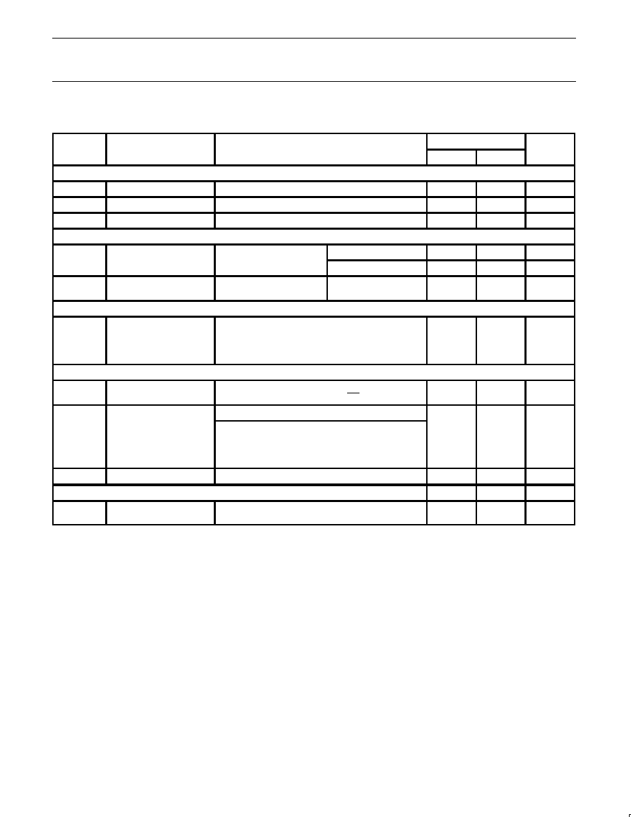
PHILIPS 22V10 FEATURES MATRIX
PL22V10-10/-15
LVT22V10-7
ABT22V10-7
ABT22V10A5
ABT22V10A7
Operating supply voltage
+4.75 to +5.25V
+3.0 to +3.6V
1
+4.75 to +5.25V
+4.75 to +5.25V
+4.75 to +5.25V
Live Insertion
No
Yes
No
Yes
Yes
Dual Verify
No
Yes
No
Yes
Yes
Metastability
No
Hardened
Immune
No
No
Source Drive Capability
4mA
(V
OH
= 2.4V)
16mA
(V
OH
= 2.0V)
16mA
(V
OH
= 2.4V)
16mA
(V
OH
= 2.4V)
16mA
(V
OH
= 2.4V)
Sink Drive Capability
16mA
(V
OL
= 0.5V)
32mA
(V
OL
= 0.5V)
48mA
(V
OL
= 0.5V)
48mA
(V
OL
= 0.5V)
48mA
(V
OL
= 0.5V)
Low Ground Bounce
No
Yes
Yes
Yes
Yes
Package Availability:
Plastic Dual In-Line (N)
24-Pin
24-Pin
24-Pin
not available
not available
Plastic Leaded Chip Carrier (A)
24-Pin
28-Pin
28-Pin
28-Pin
28-Pin
Plastic Small Outline Large (D)
24-Pin
24-Pin
not available
not available
not available
NOTE:
1. 5 volt compatible I/O. Inputs are capable of handling 7V and the outputs can also be pulled up to 7 volts.
Philips Semiconductors
Product specification
ABT22V10A5, A7
5V high-speed universal PLD device
with live insertion capability
1996 Dec 16
14
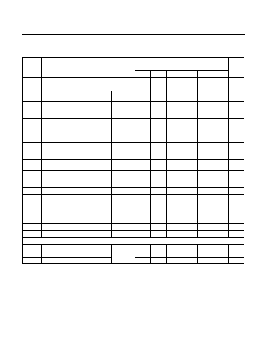
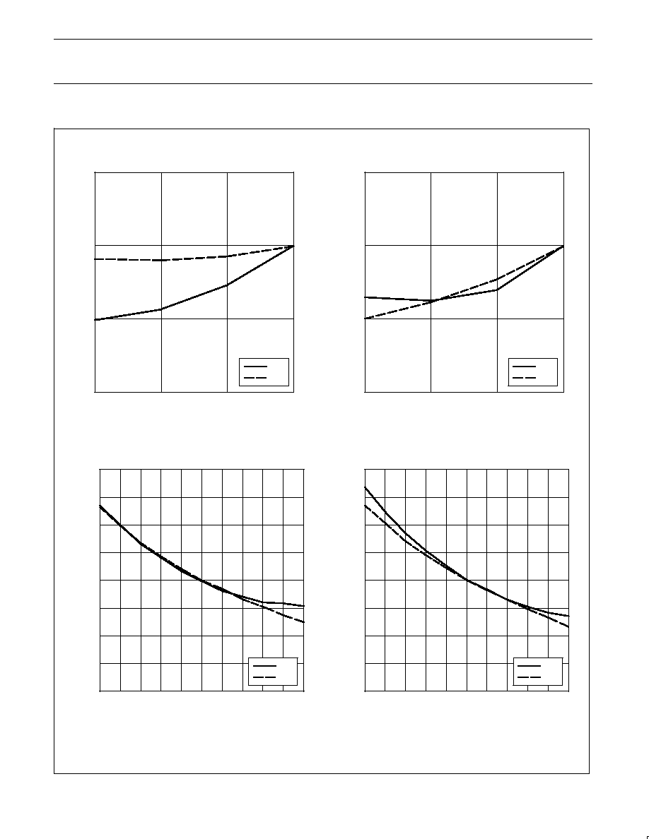
ABT22V10A5 TIMING CHARACTERIZATION
Normalized t
CO
vs Temperature
(V
CC
= 5.0V, output capacitance = 50pF, 5 outputs switching)
Normalized t
PD
vs Temperature
(V
CC
= 5.0V, output capacitance = 50pF, 5 outputs switching)
Normalized tCO vs VCC
(temp = 25
∞
C, output capacitance = 50pF, 5 outputs switching)
Temperature (
∞
C)
Temperature (
∞
C)
Supply Voltage (V)
Supply Voltage (V)
Normalized t
CO
Normalized t
PD
Normalized t
CO
Normalized t
PD
1.10
1.05
1.00
0.95
0.90
RISE
FALL
Normalized tPD vs VCC
(temp = 25
∞
C, output capacitance = 50pF, 5 outputs switching)
The timing characterization represents the average values of a representative sample for each parameter.
The data can be used to derate the MAX AC CHARACTERIZATION based upon the specific user design.
Philips guarantees the MAX AC CHARACTERIZATION specifications.
4.5
4.6
4.7
4.8
4.9
5.0
5.1
5.2
5.3
5.4
5.5
SP00370
1.10
1.00
0.90
0.80
0
25
50
75
1.10
1.00
0.90
0.80
0
25
50
75
1.10
1.05
1.00
0.95
0.90
4.5
4.6
4.7
4.8
4.9
5.0
5.1
5.2
5.3
5.4
5.5
RISE
FALL
RISE
FALL
RISE
FALL
Philips Semiconductors
Product specification
ABT22V10A5, A7
5V high-speed universal PLD device
with live insertion capability
1996 Dec 16
15
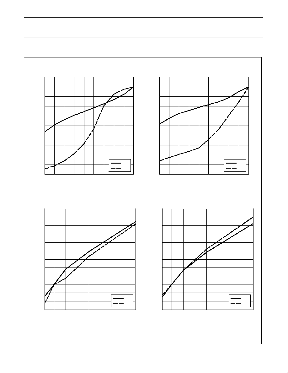
ABT22V10A5 TIMING CHARACTERIZATION
The timing characterization represents the average values of a representative sample for each parameter.
The data can be used to derate the MAX AC CHARACTERIZATION based upon the specific user design.
Philips guarantees the MAX AC CHARACTERIZATION specifications.
Delta t
CO
vs Number of Outputs Switching
(V
CC
= 5.0V, temp = 25
∞
C, output capacitance = 50pF)
Delta t
PD
vs Number of Outputs Switching
(V
CC
= 5.0V, temp = 25
∞
C, output capacitance = 50pF)
Delta t
CO
vs Output Capacitance
(V
CC
= 5.0V, temp = 25
∞
C, 5 Outputs Switching)
Delta t
PD
vs Output Capacitance
(V
CC
= 5.0V, temp = 25
∞
C, 5 Outputs Switching)
CO
PD
PD
CO
0.20
0.0
≠0.40
≠0.80
≠1.00
≠1.40
≠1.80
1
2
3
4
5
6
7
8
9
10
Number of Outputs Switching
Number of Outputs Switching
Output Capacitance
Output Capacitance
Delta t (ns)
Delta t (ns)
Delta t (ns)
Delta t (ns)
SP00371
≠0.20
≠0.60
RISE
FALL
≠1.20
≠1.60
0.20
0.0
≠0.40
≠0.80
≠1.00
≠1.40
≠1.80
1
2
3
4
5
6
7
8
9
10
≠0.20
≠0.60
≠1.20
≠1.60
RISE
FALL
10
50
100
200
400
3.50
2.50
0.50
≠1.50
4.50
1.50
≠0.50
10
50
100
200
400
3.50
2.50
0.50
≠1.50
4.50
1.50
≠0.50
RISE
FALL
RISE
FALL

Philips Semiconductors
Product specification
ABT22V10A5, A7
5V high-speed universal PLD device
with live insertion capability
1996 Dec 16
16
PLCC28:
plastic leaded chip carrer; 28 leads; pedestal
SOT261-3

Philips Semiconductors
Product specification
ABT22V10A5, A7
5V high-speed universal PLD device
with live insertion capability
1996 Dec 16
17
NOTES

Philips Semiconductors
Product specification
ABT22V10A5, A7
5V high-speed universal PLD device
with live insertion capability
1996 Dec 16
18
Philips Semiconductors and Philips Electronics North America Corporation reserve the right to make changes, without notice, in the products,
including circuits, standard cells, and/or software, described or contained herein in order to improve design and/or performance. Philips
Semiconductors assumes no responsibility or liability for the use of any of these products, conveys no license or title under any patent, copyright,
or mask work right to these products, and makes no representations or warranties that these products are free from patent, copyright, or mask
work right infringement, unless otherwise specified. Applications that are described herein for any of these products are for illustrative purposes
only. Philips Semiconductors makes no representation or warranty that such applications will be suitable for the specified use without further testing
or modification.
LIFE SUPPORT APPLICATIONS
Philips Semiconductors and Philips Electronics North America Corporation Products are not designed for use in life support appliances, devices,
or systems where malfunction of a Philips Semiconductors and Philips Electronics North America Corporation Product can reasonably be expected
to result in a personal injury. Philips Semiconductors and Philips Electronics North America Corporation customers using or selling Philips
Semiconductors and Philips Electronics North America Corporation Products for use in such applications do so at their own risk and agree to fully
indemnify Philips Semiconductors and Philips Electronics North America Corporation for any damages resulting from such improper use or sale.
This data sheet contains preliminary data, and supplementary data will be published at a later date. Philips
Semiconductors reserves the right to make changes at any time without notice in order to improve design
and supply the best possible product.
Philips Semiconductors
811 East Arques Avenue
P.O. Box 3409
Sunnyvale, California 94088≠3409
Telephone 800-234-7381
DEFINITIONS
Data Sheet Identification
Product Status
Definition
Objective Specification
Preliminary Specification
Product Specification
Formative or in Design
Preproduction Product
Full Production
This data sheet contains the design target or goal specifications for product development. Specifications
may change in any manner without notice.
This data sheet contains Final Specifications. Philips Semiconductors reserves the right to make changes
at any time without notice, in order to improve design and supply the best possible product.
Philips Semiconductors and Philips Electronics North America Corporation
register eligible circuits under the Semiconductor Chip Protection Act.
©
Copyright Philips Electronics North America Corporation 1996
All rights reserved. Printed in U.S.A.
Philips
Semiconductors