Philips
Semiconductors
74ALVCH16540
2.5V/3.3V 16-bit buffer/line driver,
inverting, 5V input tolerant (3-State)
Product specification
Supersedes data of 1996 Feb 07
IC24 Data Handbook
1997 Aug 11
INTEGRATED CIRCUITS
Philips Semiconductors
Product specification
74ALVCH16540
16-bit buffer/line driver, inverting,
5V input tolerant (3-State)
2
1997 Aug 11
853-2020 18266
FEATURES
∑
Wide supply voltage range of 1.2 V to 3.6 V
∑
Complies with JEDEC standard no. 8-1A
∑
CMOS low power consumption
∑
MULTIBYTE
TM
flow-through standard pin-out architecture
∑
Low inductance multiple V
CC
and ground pins for minimum noise
and ground bounce
∑
Direct interface with TTL levels
∑
Bus hold on all data inputs eliminates the need for external pull-up
resistors to hold unused inputs
∑
Output drive capability 50
transmission lines @ 85
∞
C
DESCRIPTION
The 74ALVCH16540 is a high-performance, low-power, low-voltage,
Si-gate CMOS device, superior to most advanced CMOS
compatible TTL families.
The 74ALVCH16540 is a 16-bit inverting buffer/line driver with
3-State outputs. The 3-State outputs are controlled by the output
enable inputs 1OE
n
and 2OE
n
. A HIGH on nOE
n
causes the outputs
to assume a high impedance OFF-state.
Active bus hold circuitry is provided to hold unused or floating data
inputs at a valid logic level. This feature eliminates the need for
external pull-up or pull-down resistors. The device can be used as
four 4-bit buffers, two 8-bit buffers or one 16-bit buffer.
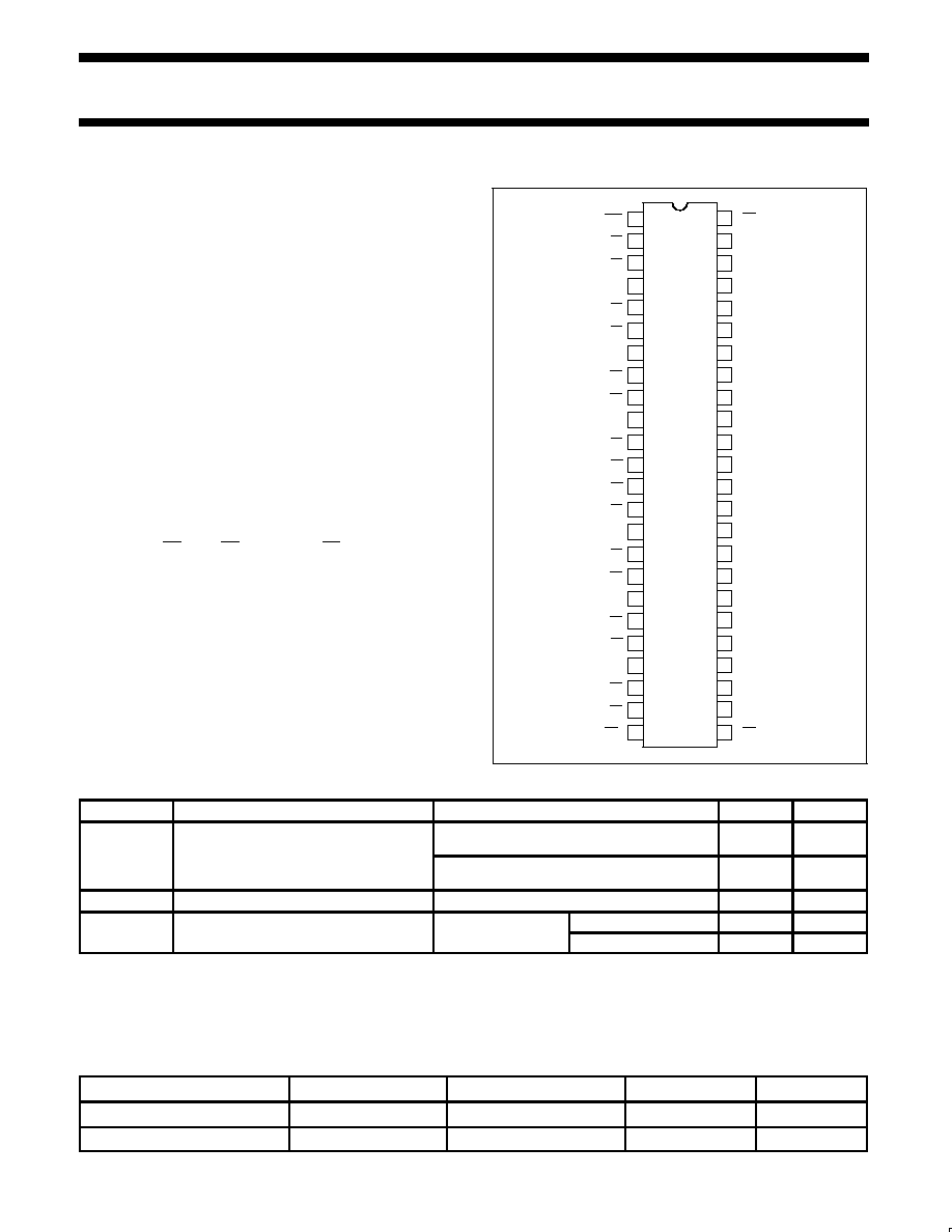
PIN CONFIGURATION
1
2
3
4
5
6
7
8
9
10
11
12
13
14
15
16
17
18
19
20
29
30
31
32
33
34
35
36
37
38
39
40
41
42
43
44
45
46
47
48
1OE
1
1Y0
1Y1
GND
1Y2
1Y3
V
CC
1Y5
GND
1Y6
1Y7
2Y0
2Y1
GND
1Y4
2Y2
2Y3
V
CC
2Y4
2Y5
2A5
2A4
V
CC
2A3
2A2
GND
2A1
2A0
1A7
1A6
GND
1A5
1A4
V
CC
1A3
1A2
GND
1A1
1A0
1OE
2
21
22
23
24
25
26
27
28
GND
2Y6
2Y7
2OE
1
2OE
2
2A7
2A6
GND
SW00108
QUICK REFERENCE DATA
GND = 0V; T
amb
= 25
∞
C; t
r
= t
f
2.5ns
SYMBOL
PARAMETER
CONDITIONS
TYPICAL
UNIT
t
/t
Propagation delay
1An to 1Yn;
C
L
= 50pF
V
CC
= 3.3V
1.8
ns
t
PHL
/t
PLH
1An to 1Yn;
2An to 2Yn
C
L
= 30pF
V
CC
= 2.5V
1.8
ns
C
I
Input capacitance
5.0
pF
C
Power dissipation capacitance per buffer
V = GND to V
CC
1
Outputs enabled
26
pF
C
PD
Power dissipation capacitance per buffer
V
I
= GND to V
CC
1
Outputs disabled
5
pF
NOTES:
1. C
PD
is used to determine the dynamic power dissipation (P
D
in
m
W):
P
D
= C
PD
◊
V
CC
2
◊
f
i
+
S
(C
L
◊
V
CC
2
◊
f
o
) where:
f
i
= input frequency in MHz; C
L
= output load capacitance in pF;
f
o
= output frequency in MHz; V
CC
= supply voltage in V;
S
(C
L
◊
V
CC
2
◊
f
o
) = sum of outputs.
ORDERING INFORMATION
PACKAGES
TEMPERATURE RANGE
OUTSIDE NORTH AMERICA
NORTH AMERICA
DWG NUMBER
48-Pin Plastic SSOP Type III
≠40
∞
C to +85
∞
C
74ALVCH16540 DL
ACH16540 DL
SOT370-1
48-Pin Plastic TSSOP Type II
≠40
∞
C to +85
∞
C
74ALVCH16540 DGG
ACH16540 DGG
SOT362-1
Philips Semiconductors
Product specification
74ALVCH16540
16-bit buffer/line driver, inverting,
5V input tolerant (3-State)
1997 Aug 11
3
PIN DESCRIPTION
PIN NUMBER
SYMBOL
NAME AND FUNCTION
1, 24
nOE
1
Output enable input
(active LOW)
2, 3, 5, 6, 8, 9,
11, 12
1Y0 to 1Y7
Data outputs
13, 14, 16, 17,
19, 20, 22, 23
2Y0 to 2Y7
Data outputs
4, 10, 15, 21,
28, 34, 39, 45
GND
Ground (0V)
7, 18, 31, 42
V
CC
Positive supply voltage
25, 48
nOE
2
Output enable input
(active LOW)
36, 35, 33, 32,
30, 29, 27, 26
2A0 to 2A7
Data inputs
47, 46, 44, 43,
41, 40, 38, 37
1A0 to 1A7
Data inputs
LOGIC SYMBOL
1A0
47
2
1Y0
1A1
46
3
1Y1
1A2
44
5
1Y2
1A3
43
6
1Y3
1A4
41
8
1Y4
1A5
40
9
1Y5
1A6
38
11
1Y6
1A7
37
12
1Y7
1OE
1
1
1OE
2
48
2A0
36
13
2Y0
2A1
35
14
2Y1
2A2
33
16
2Y2
2A3
32
17
2Y3
2A4
30
19
2Y4
2A5
29
20
2Y5
2A6
27
22
2Y6
2A7
26
23
2Y7
2OE
1
24
2OE
2
25
SW00109
FUNCTION TABLE
INPUTS
OUTPUT
nOE
1
nOE
2
nAn
nYn
L
L
L
H
L
L
H
L
X
H
X
Z
H
X
X
Z
H = HIGH voltage level
L = LOW voltage level
X = don't care
Z = high impedance OFF-state
LOGIC SYMBOL (IEEE/IEC)
48
1
46
44
43
41
40
38
37
36
EN2
1
2
1
1
25
24
47
35
33
32
30
29
27
26
3
2
5
6
8
9
11
12
13
14
16
17
19
20
22
23
SW00110
1OE
1
1OE
2
2OE
1
2OE
2
1A0
1A1
1A2
1A3
1A4
1A5
1A6
2A0
2A1
2A2
2A3
2A4
2A5
2A6
2A7
1Y0
1Y1
1Y2
1Y3
1Y4
1Y5
1Y6
1Y7
2Y0
2Y1
2Y2
2Y3
2Y4
2Y7
1A7
2Y5
2Y6
&
&
EN1
BUS HOLD CIRCUIT
To internal circuit
V
CC
Data Input
SW00044
Philips Semiconductors
Product specification
74ALVCH16540
16-bit buffer/line driver, inverting,
5V input tolerant (3-State)
1997 Aug 11
4
RECOMMENDED OPERATING CONDITIONS
SYMBOL
PARAMETER
CONDITIONS
LIMITS
UNIT
SYMBOL
PARAMETER
CONDITIONS
MIN
MAX
UNIT
DC supply voltage 2.5V range (for max. speed
performance)
2.3
2.7
V
CC
DC supply voltage 3.3V range (for max. speed
performance)
3.0
3.6
V
DC supply voltage (for low-voltage applications)
1.2
3.6
V
DC Input voltage range
For data input pins
0
V
CC
V
V
I
DC Input voltage range
For control pins
0
5.5
V
V
O
DC output voltage range
0
V
CC
V
T
amb
Operating free-air temperature range
≠40
+85
∞
C
t
r
, t
f
Input rise and fall times
V
CC
= 2.3 to 3.0V
V
CC
= 3.0 to 3.6V
0
0
20
10
ns/V
ABSOLUTE MAXIMUM RATINGS
1, 2
In accordance with the Absolute Maximum Rating System (IEC 134)
Voltages are referenced to GND (ground = 0V)
SYMBOL
PARAMETER
CONDITIONS
RATING
UNIT
V
CC
DC supply voltage
≠0.5 to +4.6
V
I
IK
DC input diode current
V
I
t
0
≠50
mA
V
I
DC input voltage
For control pins and data inputs of ALVC
parts
2
≠0.5 to +5.5
V
I
g
For data inputs of ALVCH parts
2
≠0.5 to V
CC
+0.5
I
OK
DC output diode current
V
O
u
V
CC
or V
O
t
0
"
50
mA
V
O
DC output voltage
Note 2
≠0.5 to V
CC
+0.5
V
I
O
DC output source or sink current
V
O
= 0 to V
CC
"
50
mA
I
GND
, I
CC
DC V
CC
or GND current
"
100
mA
T
stg
Storage temperature range
≠65 to +150
∞
C
P
TOT
Power dissipation per package
≠plastic medium-shrink SO (SSOP)
≠plastic mini-pack (TSSOP)
For temperature range: ≠40 to +125
∞
C
above +55
∞
C derate linearly with 11.3 mW/K
above +55
∞
C derate linearly with 8 mW/K
850
600
mW
NOTES:
1. Stresses beyond those listed may cause permanent damage to the device. These are stress ratings only and functional operation of the
device at these or any other conditions beyond those indicated under "recommended operating conditions" is not implied. Exposure to
absolute-maximum-rated conditions for extended periods may affect device reliability.
2. The input and output voltage ratings may be exceeded if the input and output current ratings are observed.

Philips Semiconductors
Product specification
74ALVCH16540
16-bit buffer/line driver, inverting,
5V input tolerant (3-State)
1997 Aug 11
5
DC ELECTRICAL CHARACTERISTICS
LIMITS
SYMBOL
PARAMETER
TEST CONDITIONS
Temp = -40
∞
C to +85
∞
C
UNIT
MIN
TYP
1
MAX
V
CC
= 1.2V
V
CC
V
IH
HIGH level Input voltage
V
CC
= 2.3 to 2.7V
1.7
V
V
CC
= 2.7 to 3.6V
2.0
V
CC
= 1.2V
GND
V
IL
LOW level Input voltage
V
CC
= 2.3 to 2.7V
0.7
V
V
CC
= 2.7 to 3.6V
0.8
V
CC
= 2.3V; V
I
= V
IH
or V
IL
; I
O
= ≠1mA
V
CC
*
0.3
V
CC
= 2.3V; V
I
= V
IH
or V
IL
; I
O
= ≠8mA
V
CC
*
0.5
V
OH
HIGH level output voltage
V
CC
= 2.7V; V
I
= V
IH
or V
IL
; I
O
= ≠12mA
V
CC
*
0.5
V
V
CC
= 2.3/3.0V; V
I
= V
IH
or V
IL
; I
O
= ≠100
µ
A
V
CC
*
0.2
V
CC
V
CC
= 3.0V; V
I
= V
IH
or V
IL;
I
O
= ≠24mA
V
CC
*
1.0
V
CC
= 2.3V; V
I
= V
IH
or V
IL
; I
O
= 1mA
0.40
V
CC
= 2.3V; V
I
= V
IH
or V
IL
; I
O
= 8mA
0.60
V
OL
LOW level output voltage
V
CC
= 2.7V; V
I
= V
IH
or V
IL
; I
O
= 12mA
0.40
V
V
CC
= 2.3/3.0V; V
I
= V
IH
or V
IL
; I
O
= 100
µ
A
0.20
V
CC
= 3.0V; V
I
= V
IH
or V
IL;
I
O
= 24mA
0.55
V
CC
= 3 6V; V = 5 5V or GND
Control pins
"
0 1
"
5
I
Input leakage current
V
CC
= 3.6V; V
I
= 5.5V or GND
Control pins
"
0.1
"
5
µ
A
I
I
Input leakage current
V
CC
= 3.6V; V
I
= V
CC
or GND
Data input pins
"
0.1
"
5
µ
A
I
IHZ
/I
ILZ
Input current for common I/O pins
V
CC
= 3.6V; V
I
= V
CC
or GND
"
0.1
"
15
µ
A
I
O
3-State output OFF-state current
V
CC
= 3.6V; V
I
= V
IH
or V
IL
; V
O
= V
CC
or GND
0.1
"
10
µ
A
I
OZ
3-State output OFF-state current
V
CC
= 2.7V; V
I
= V
IH
or V
IL
; V
O
= V
CC
or GND
0.1
"
5
µ
A
I
CC
Quiescent supply current
V
CC
= 3.6V; V
I
= V
CC
or GND; I
O
= 0
0.2
40
µ
A
I
CC
Quiescent supply current
V
CC
= 2.7V; V
I
= V
CC
or GND; I
O
= 0
0.2
20
µ
A
I
CC
Additional quiescent supply current per
control pin
V
CC
= 2.7V to 3.6V; V
I
= V
CC
≠0.6V; I
O
= 0
5
500
µ
A
I
CC
Additional quiescent supply current per
data I/O pin
V
CC
= 2.7V to 3.6V; V
I
= V
CC
≠0.6V; I
O
= 0
150
750
µ
A
IBHL
Bus hold LOW sustaining current
V
CC
= 2.3V; V
I
= 0.7V
45
µ
A
IBHL
Bus hold LOW sustaining current
V
CC
= 3.0V; V
I
= 0.8V
75
µ
A
IBHH
Bus hold HIGH sustaining current
V
CC
= 2.3V; V
I
= 1.7V
≠45
µ
A
IBHH
Bus hold HIGH sustaining current
V
CC
= 3.0V; V
I
= 2.0V
≠75
µ
A
IBHLO
Bus hold LOW overdrive current
V
CC
= 2.7V
300
µ
A
IBHLO
Bus hold LOW overdrive current
V
CC
= 3.6V
450
µ
A
IBHHO
Bus hold HIGH overdrive current
V
CC
= 2.7V
≠300
µ
A
IBHHO
Bus hold HIGH overdrive current
V
CC
= 3.6V
≠450
µ
A
NOTES:
1. All typical values are at V
CC
= 3.3V and T
amb
= 25
∞
C.

Philips Semiconductors
Product specification
74ALVCH16540
16-bit buffer/line driver, inverting,
5V input tolerant (3-State)
1997 Aug 11
6
AC CHARACTERISTICS FOR V
CC
= 3.0V TO 3.6V RANGE AND V
CC
= 2.7V
GND = 0V; t
r
= t
f
2.5ns; C
L
= 50pF
LIMITS
SYMBOL
PARAMETER
WAVEFORM
V
CC
= 3.0
±
0.3V
V
CC
= 2.7V
UNIT
MIN
TYP
1
MAX
TYP
MAX
t
PHL
/t
PLH
Propagation delay
1An to 1Yn;
2An to 2Yn
4
1.8
3.0
2.1
3.6
ns
t
PZH
/t
PZL
3-State output enable time
1OEn to 1Yn;
2OEn to 2Yn
5, 6
2.1
3.8
2.9
4.7
ns
t
PHZ
/t
PLZ
3-State output disable time
1OEn to 1Yn;
2OEn to 2Yn
5, 6
2.7
4.1
3.2
4.5
ns
NOTE:
1. All typical values are at V
CC
= 3.3V and T
amb
= 25
∞
C.
AC CHARACTERISTICS FOR V
CC
= 2.3V TO 2.7V RANGE AND V
CC
< 2.3V
GND = 0V; t
r
= t
f
2.0ns; C
L
= 30pF
LIMITS
SYMBOL
PARAMETER
WAVEFORM
V
CC
= 2.3 to 2.7V
V
CC
= 1.8V
V
CC
= 1.2V
UNIT
MIN
TYP
1
MAX
TYP
MAX
t
PHL
/t
PLH
Propagation delay
1An to 1Yn;
2An to 2Yn
4
1.8
3.2
3.1
6.0
ns
t
PZH
/t
PZL
3-State output enable time
1OEn to 1Yn;
2OEn to 2Yn
5, 6
2.5
4.4
4.3
8.9
ns
t
PHZ
/t
PLZ
3-State output disable time
1OEn to 1Yn;
2OEn to 2Yn
5, 6
2.2
3.8
3.6
6.4
ns
NOTE:
1. All typical values are at V
CC
= 2.5V and T
amb
= 25
∞
C.
AC WAVEFORMS FOR V
CC
= 3.0V TO 3.6V AND V
CC
= 2.7V RANGE
V
M
= 1.5 V
V
X
= V
OL
+ 0.3V
V
Y
= V
OH
≠0.3V
V
OL
and V
OH
are the typical output voltage drop that occur with the
output load.
V
I
= 2.7V
SW00111
nAn
INPUT
V
M
tPHL
tPLH
V
OL
V
I
V
M
GND
V
OH
nYn
OUTPUT
Waveform 1. Input (An) to output (Yn) propagation delay times
t
PLZ
t
PZL
V
I
OE INPUT
GND
V
CC
Y OUTPUT
LOW-to-OFF
OFF-to-LOW
V
OL
V
OH
Y OUTPUT
HIGH-to-OFF
OFF-to-HIGH
GND
outputs
enabled
outputs
enabled
outputs
disabled
t
PHZ
V
M
V
M
V
M
t
PZH
V
X
V
Y
SW00112
Waveform 2. 3-State enable and disable times

Philips Semiconductors
Product specification
74ALVCH16540
16-bit buffer/line driver, inverting,
5V input tolerant (3-State)
1997 Aug 11
7
TEST CIRCUIT
PULSE
GENERATOR
RT
VIN
D.U.T.
VOUT
CL
VCC
R
L
=500
SWITCH POSITION
TEST
SWITCH
t
PLH
/t
PHL
Open
t
PLZ
/t
PZL
2
<
V
CC
t
PHZ
/t
PZH
GND
Test Circuit for 3-State Outputs
Open
GND
S
1
2
<
V
CC
DEFINITIONS
V
CC
t
2.7V
2.7 ≠ 3.6V
V
IN
V
CC
2.7V
R
L
= Load resistor
C
L
= Load capacitance includes jig and probe capacitance
R
T
= Termination resistance should be equal to Z
OUT
of pulse generators.
SW00047
R
L
=500
Waveform 3. Load circuitry for switching times
AC WAVEFORMS FOR V
CC
= 2.3V TO 2.7V AND V
CC
< 2.3V RANGE
V
M
= 0.5 * V
CC
V
X
= V
OL
+ 0.15V
V
Y
= V
OH
≠0.15V
V
OL
and V
OH
are the typical output voltage drop that occur with the
output load.
V
I
= V
CC
SW00111
nAn
INPUT
V
M
tPHL
tPLH
V
OL
V
I
V
M
GND
V
OH
nYn
OUTPUT
Waveform 4. Input (An) to output (Yn) propagation delay times
t
PLZ
t
PZL
V
I
OE INPUT
GND
V
CC
Y OUTPUT
LOW-to-OFF
OFF-to-LOW
V
OL
V
OH
Y OUTPUT
HIGH-to-OFF
OFF-to-HIGH
GND
outputs
enabled
outputs
enabled
outputs
disabled
t
PHZ
V
M
V
M
V
M
t
PZH
V
X
V
Y
SW00112
Waveform 5. 3-State enable and disable times

Philips Semiconductors
Product specification
74ALVCH16540
16-bit buffer/line driver, inverting,
5V input tolerant (3-State)
1997 Aug 11
8
TEST CIRCUIT
PULSE
GENERATOR
RT
VIN
D.U.T.
VOUT
CL
VCC
R
L
=500
SWITCH POSITION
TEST
SWITCH
t
PLH
/t
PHL
Open
t
PLZ
/t
PZL
2
<
V
CC
t
PHZ
/t
PZH
GND
Test Circuit for 3-State Outputs
Open
GND
S
1
2
<
V
CC
DEFINITIONS
V
CC
t
2.7V
2.7 ≠ 3.6V
V
IN
V
CC
2.7V
R
L
= Load resistor
C
L
= Load capacitance includes jig and probe capacitance
R
T
= Termination resistance should be equal to Z
OUT
of pulse generators.
SW00047
R
L
=500
Waveform 6. Load circuitry for switching times

Philips Semiconductors
Product specification
74ALVCH16540
2.5V/3.3V 16-bit buffer/line driver, inverting,
5V input tolerant (3-State)
1997 Aug 11
9
SSOP48:
plastic shrink small outline package; 48 leads; body width 7.5 mm
SOT370-1

Philips Semiconductors
Product specification
74ALVCH16540
2.5V/3.3V 16-bit buffer/line driver, inverting,
5V input tolerant (3-State)
1997 Aug 11
10
TSSOP48:
plastic thin shrink small outline package; 48 leads; body width 6.1mm
SOT362-1

Philips Semiconductors
Product specification
74ALVCH16540
2.5V/3.3V 16-bit buffer/line driver, inverting,
5V input tolerant (3-State)
1997 Aug 11
11
NOTES
Philips Semiconductors
Product specification
74ALVCH16540
2.5V/3.3V 16-bit buffer/line driver, inverting,
5V input tolerant (3-State)
1997 Aug 11
12
Philips Semiconductors and Philips Electronics North America Corporation reserve the right to make changes, without notice, in the products,
including circuits, standard cells, and/or software, described or contained herein in order to improve design and/or performance. Philips
Semiconductors assumes no responsibility or liability for the use of any of these products, conveys no license or title under any patent, copyright,
or mask work right to these products, and makes no representations or warranties that these products are free from patent, copyright, or mask
work right infringement, unless otherwise specified. Applications that are described herein for any of these products are for illustrative purposes
only. Philips Semiconductors makes no representation or warranty that such applications will be suitable for the specified use without further testing
or modification.
LIFE SUPPORT APPLICATIONS
Philips Semiconductors and Philips Electronics North America Corporation Products are not designed for use in life support appliances, devices,
or systems where malfunction of a Philips Semiconductors and Philips Electronics North America Corporation Product can reasonably be expected
to result in a personal injury. Philips Semiconductors and Philips Electronics North America Corporation customers using or selling Philips
Semiconductors and Philips Electronics North America Corporation Products for use in such applications do so at their own risk and agree to fully
indemnify Philips Semiconductors and Philips Electronics North America Corporation for any damages resulting from such improper use or sale.
This data sheet contains preliminary data, and supplementary data will be published at a later date. Philips
Semiconductors reserves the right to make changes at any time without notice in order to improve design
and supply the best possible product.
Philips Semiconductors
811 East Arques Avenue
P.O. Box 3409
Sunnyvale, California 94088≠3409
Telephone 800-234-7381
DEFINITIONS
Data Sheet Identification
Product Status
Definition
Objective Specification
Preliminary Specification
Product Specification
Formative or in Design
Preproduction Product
Full Production
This data sheet contains the design target or goal specifications for product development. Specifications
may change in any manner without notice.
This data sheet contains Final Specifications. Philips Semiconductors reserves the right to make changes
at any time without notice, in order to improve design and supply the best possible product.
©
Copyright Philips Electronics North America Corporation 1998
All rights reserved. Printed in U.S.A.
Date of release: 08≠97
Document order number:
9397-750-04545
Philips
Semiconductors