1.
Product profile
1.1 General description
Planar PIN diode in a SOD882 ultra small SMD plastic package.
1.2 Features
s
High voltage, current controlled RF resistor
s
Low losses at very low currents
s
Low diode capacitance
s
Very low series inductance
s
For applications up to 3 GHz.
1.3 Applications
s
RF attenuators and switches.
2.
Pinning information
[1]
Package marked by a masking bar.
3.
Ordering information
BAP142L
Silicon PIN diode
Rev. 01 -- 27 May 2004
Preliminary data sheet
Table 1:
Discrete pinning
Pin
Description
Simplified outline
Symbol
1
cathode
[1]
2
anode
Transparent top view
SOD882
1
2
sym006
Table 2:
Ordering information
Type number
Package
Name
Description
Version
BAP142L
-
Leadless ultra small plastic package; 2 terminals;
body 1.0
�
0.6
�
0.5 mm
SOD882

9397 750 13056
� Koninklijke Philips Electronics N.V. 2004. All rights reserved.
Preliminary data sheet
Rev. 01 -- 27 May 2004
2 of 8
Philips Semiconductors
BAP142L
Silicon PIN diode
4.
Marking
5.
Limiting values
6.
Thermal characteristics
7.
Characteristics
Table 3:
Marking
Type number
Marking code
BAP142L
E1
Table 4:
Limiting values
In accordance with the Absolute Maximum Rating System (IEC 60134).
Symbol
Parameter
Conditions
Min
Max
Unit
V
R
continuous reverse voltage
-
50
V
I
F
continuous forward current
-
100
mA
P
tot
total power dissipation
T
s
= 90
�
C
-
315
mW
T
stg
storage temperature
-
65
+150
�
C
T
j
junction temperature
-
65
+150
�
C
Table 5:
Thermal characteristics
Symbol
Parameter
Conditions
Typ
Unit
R
th(j-s)
thermal resistance from junction
to soldering point
190
K/W
Table 6:
Electrical characteristics
T
j
= 25
�
C unless otherwise specified.
Symbol
Parameter
Conditions
Min
Typ
Max
Unit
V
F
forward voltage
I
F
= 50 mA
-
0.95
1.1
V
I
R
reverse current
V
R
= 50 V
-
-
100
nA
V
R
= 20 V
-
-
20
nA
C
d
diode capacitance
f = 1 MHz; see
Figure 2
V
R
= 0 V
-
0.26
-
pF
V
R
= 1 V
-
0.23
0.35
pF
V
R
= 20 V
-
0.17
0.25
pF
r
D
diode forward resistance
f = 100 MHz; see
Figure 1
I
F
= 0.5 mA
-
3.3
5.0
I
F
= 1 mA
-
2.4
3.6
I
F
= 10 mA
-
1.0
1.5
I
F
= 100 mA
-
0.6
0.9
9397 750 13056
� Koninklijke Philips Electronics N.V. 2004. All rights reserved.
Preliminary data sheet
Rev. 01 -- 27 May 2004
3 of 8
Philips Semiconductors
BAP142L
Silicon PIN diode
s
21
2
isolation
V
R
= 0 V; see
Figure 4
f = 900 MHz
-
16.0
-
dB
f = 1800 MHz
-
11.6
-
dB
f = 2450 MHz
-
9.9
-
dB
s
21
2
insertion loss
I
F
= 0.5 mA; see
Figure 3
f = 900 MHz
-
0.24
-
dB
f = 1800 MHz
-
0.25
-
dB
f = 2450 MHz
-
0.26
-
dB
s
21
2
insertion loss
I
F
= 1 mA; see
Figure 3
f = 900 MHz
-
0.18
-
dB
f = 1800 MHz
-
0.19
-
dB
f = 2450 MHz
-
0.21
-
dB
s
21
2
insertion loss
I
F
= 10 mA; see
Figure 3
f = 900 MHz
-
0.10
-
dB
f = 1800 MHz
-
0.11
-
dB
f = 2450 MHz
-
0.14
-
dB
s
21
2
insertion loss
I
F
= 100 mA; see
Figure 3
f = 900 MHz
-
0.07
-
dB
f = 1800 MHz
-
0.09
-
dB
f = 2450 MHz
-
0.11
-
dB
L
charge carrier life time
when switched from
I
F
= 10 mA to I
R
= 6 mA;
R
L
= 100
;
measured at I
R
= 3 mA
-
0.12
-
�
s
L
S
series inductance
I
F
= 100 mA; f = 100 MHz
-
0.6
-
nH
Table 6:
Electrical characteristics
...continued
T
j
= 25
�
C unless otherwise specified.
Symbol
Parameter
Conditions
Min
Typ
Max
Unit
9397 750 13056
� Koninklijke Philips Electronics N.V. 2004. All rights reserved.
Preliminary data sheet
Rev. 01 -- 27 May 2004
4 of 8
Philips Semiconductors
BAP142L
Silicon PIN diode
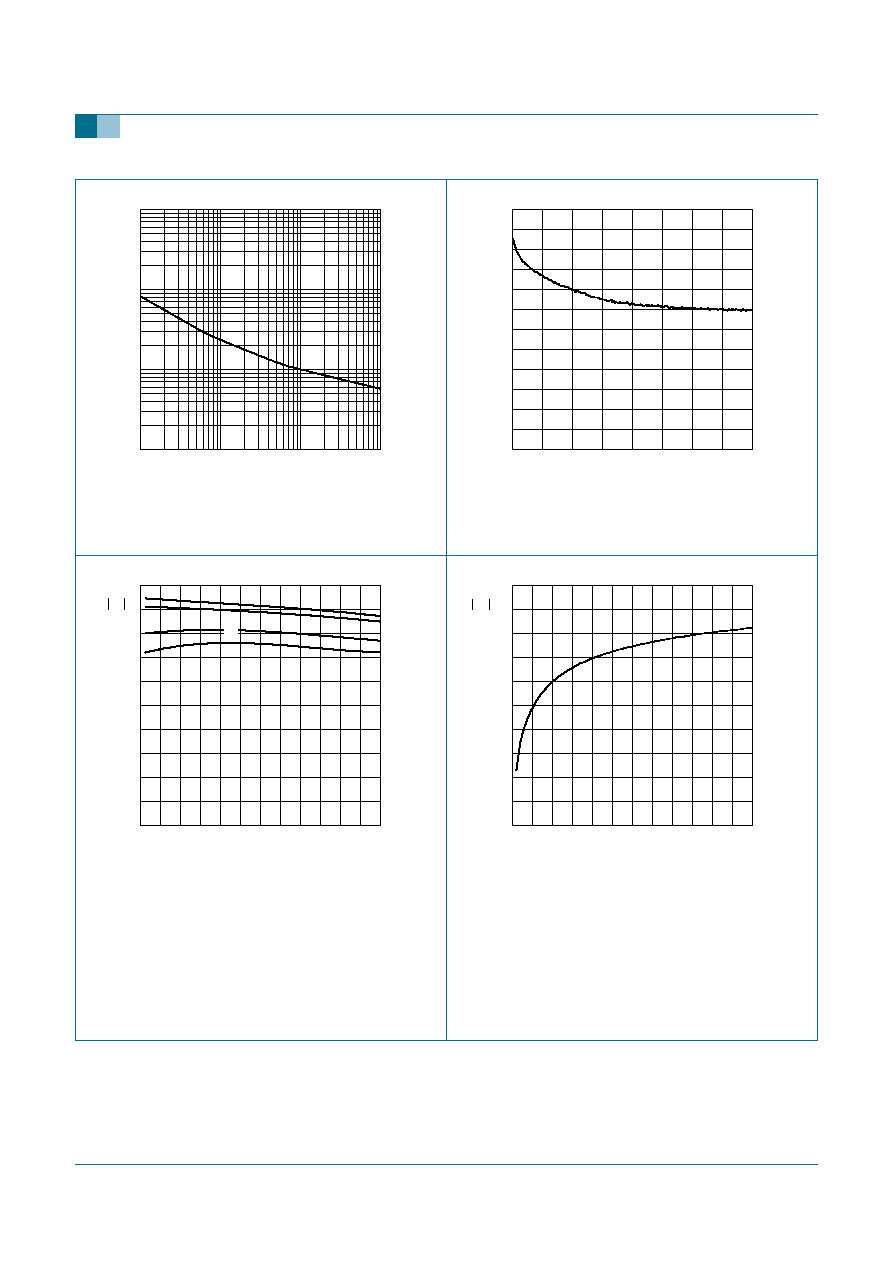
f = 100 MHz; T
j
= 25
�
C.
f = 1 MHz; T
j
= 25
�
C.
Fig 1.
Forward resistance as a function of forward
current; typical values.
Fig 2.
Diode capacitance as a function of reverse
voltage; typical values.
(1) I
F
= 100 mA.
(2) I
F
= 10 mA.
(3) I
F
= 1 mA.
(4) I
F
= 0.5 mA.
Diode inserted in series with a 50
stripline circuit
and biased via the analyzer Tee network;
T
amb
= 25
�
C.
Diode zero biased and inserted in a 50
microstrip
circuit; T
amb
= 25
�
C.
Fig 3.
Insertion loss (
|
s
21
|
2
) of the diode as a function
of frequency; typical values.
Fig 4.
Isolation (
|
s
21
|
2
) of the diode as a function of
frequency; typical values.
I
F
(mA)
10
-1
10
2
10
1
001aaa693
10
1
10
2
r
D
(
)
10
-
1
V
R
(V)
0
20
15
5
10
001aaa694
100
200
300
C
D
(fF)
0
001aaa695
f (GHz)
0
3
2
1
-
0.6
-
0.4
-
0.8
-
0.2
0
s
21
2
(dB)
-
1
(2)
(4)
(1)
(3)
001aaa696
f (GHz)
0
3
2
1
-
30
-
20
-
40
-
10
0
-
50
s
21
2
(dB)
9397 750 13056
� Koninklijke Philips Electronics N.V. 2004. All rights reserved.
Preliminary data sheet
Rev. 01 -- 27 May 2004
5 of 8
Philips Semiconductors
BAP142L
Silicon PIN diode
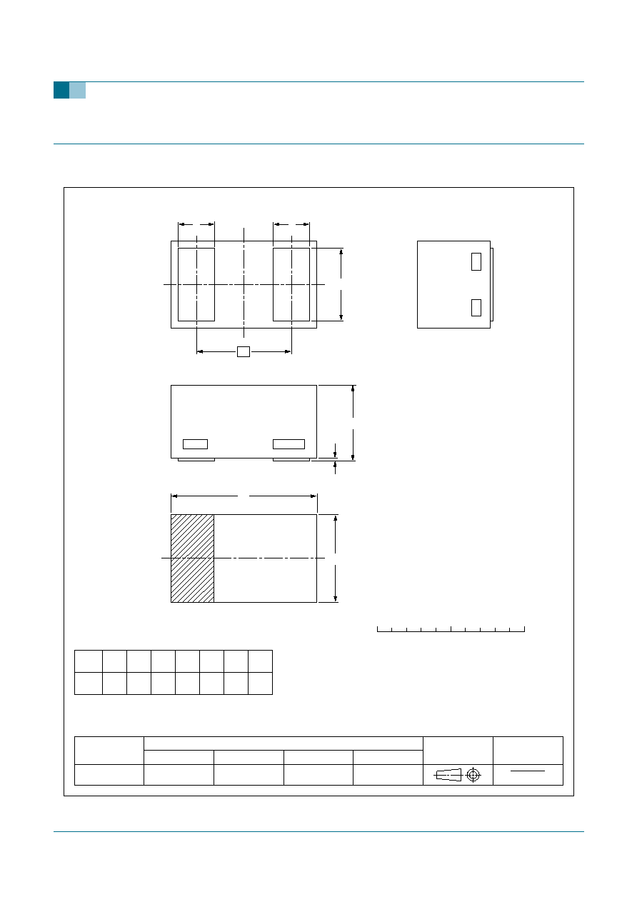
8.
Package outline
Fig 5.
Package outline.
UNIT
A
1
max.
A
(1)
b
e
1
L
REFERENCES
OUTLINE
VERSION
EUROPEAN
PROJECTION
ISSUE DATE
IEC
JEDEC
JEITA
mm
0.50
0.46
0.55
0.47
0.03
0.62
0.55
0.65
DIMENSIONS (mm are the original dimensions)
Notes
1. Including plating thickness
2. The marking bar indicates the cathode
0.30
0.22
SOD882
03-04-16
03-04-17
D
E
1.02
0.95
L
E
(2)
2
1
b
A1
A
D
L
Leadless ultra small plastic package; 2 terminals; body 1.0 x 0.6 x 0.5 mm
SOD882
0
0.5
1 mm
scale
e1