 | –≠–ª–µ–∫—Ç—Ä–æ–Ω–Ω—ã–π –∫–æ–º–ø–æ–Ω–µ–Ω—Ç: BAP63-02 | –°–∫–∞—á–∞—Ç—å:  PDF PDF  ZIP ZIP |
DATA SHEET
Product specification
Supersedes data of 2001 Apr 04
2001 May 18
DISCRETE SEMICONDUCTORS
BAP63-02
Silicon PIN diode
M3D319
2001 May 18
2
Philips Semiconductors
Product specification
Silicon PIN diode
BAP63-02
FEATURES
∑
High speed switching for RF signals
∑
Low diode capacitance
∑
Low diode forward resistance
∑
Very low series inductance
∑
For applications up to 3 GHz.
APPLICATIONS
∑
RF attenuators and switches.
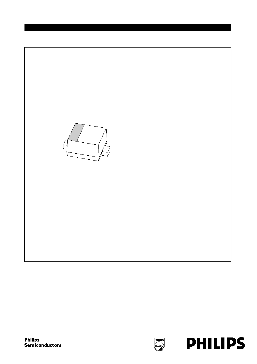
DESCRIPTION
Planar PIN diode in a SOD523 ultra small SMD plastic
package.
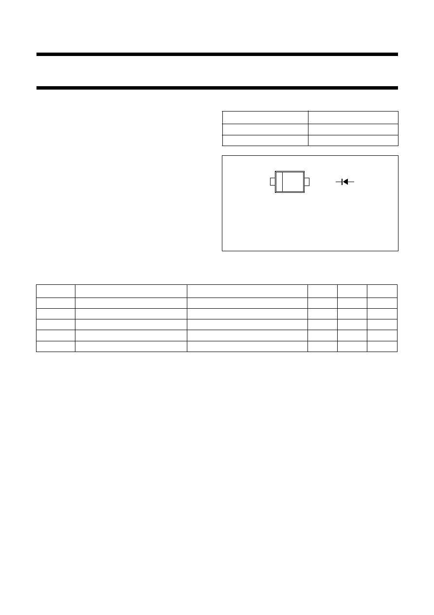
PINNING
PIN
DESCRIPTION
1
cathode
2
anode
Marking code: K5.
Fig.1 Simplified outline (SOD523) and symbol.
handbook, halfpage
1
2
Top view
MAM405
LIMITING VALUES
In accordance with the Absolute Maximum Rating System (IEC 60134).
SYMBOL
PARAMETER
CONDITIONS
MIN.
MAX.
UNIT
V
R
continuous reverse voltage
-
50
V
I
F
continuous forward current
-
100
mA
P
tot
total power dissipation
T
s
90
∞
C
-
715
mW
T
stg
storage temperature
-
65
+150
∞
C
T
j
junction temperature
-
65
+150
∞
C
2001 May 18
3
Philips Semiconductors
Product specification
Silicon PIN diode
BAP63-02
ELECTRICAL CHARACTERISTICS
T
j
= 25
∞
C unless otherwise specified.
Note
1. Guaranteed on AQL basis: inspection level S4, AQL 1.0.
THERMAL CHARACTERISTICS
SYMBOL
PARAMETER
CONDITIONS
TYP.
MAX.
UNIT
V
F
forward voltage
I
F
= 50 mA
0.95
1.1
V
I
R
reverse leakage current
V
R
= 35 V
-
10
nA
C
d
diode capacitance
V
R
= 0; f = 1 MHz
0.36
-
pF
V
R
= 1 V; f = 1 MHz
0.32
-
pF
V
R
= 20 V; f = 1 MHz
0.25
0.32
pF
r
D
diode forward resistance
I
F
= 0.5 mA; f = 100 MHz; note 1
2.5
3.5
I
F
= 1 mA; f = 100 MHz; note 1
1.95
3
I
F
= 10 mA; f = 100 MHz; note 1
1.17
1.8
I
F
= 100 mA; f = 100 MHz; note 1
0.9
1.5
|
s
21
|
2
isolation
V
R
= 0; f = 900 MHz
15.6
-
dB
V
R
= 0; f = 1800 MHz
10.3
-
dB
V
R
= 0; f = 2450 MHz
8.3
-
dB
|
s
21
|
2
insertion loss
I
F
= 0.5 mA; f = 900 MHz
0.19
-
dB
I
F
= 0.5 mA; f = 1800 MHz
0.24
-
dB
I
F
= 0.5 mA; f = 2450 MHz
0.28
-
dB
|
s
21
|
2
insertion loss
I
F
= 1 mA; f = 900 MHz
0.16
-
dB
I
F
= 1 mA; f = 1800 MHz
0.20
-
dB
I
F
= 1 mA; f = 2450 MHz
0.25
-
dB
|
s
21
|
2
insertion loss
I
F
= 10 mA; f = 900 MHz
0.10
-
dB
I
F
= 10 mA; f = 1800 MHz
0.16
-
dB
I
F
= 10 mA; f = 2450 MHz
0.20
-
dB
|
s
21
|
2
insertion loss
I
F
= 100 mA; f = 900 MHz
0.09
-
dB
I
F
= 100 mA; f = 1800 MHz
0.14
-
dB
I
F
= 100 mA; f = 2450 MHz
0.18
-
dB
L
charge carrier life time
when switched from I
F
= 10 mA to
I
R
= 6 mA; R
L
= 100
;
measured at I
R
= 3 mA
310
-
ns
L
S
series inductance
I
F
= 100 mA; f = 100 MHz
0.6
-
nH
SYMBOL
PARAMETER
VALUE
UNIT
R
th j-s
thermal resistance from junction to soldering point
85
K/W

2001 May 18
4
Philips Semiconductors
Product specification
Silicon PIN diode
BAP63-02
GRAPHICAL DATA
handbook, halfpage
10
1
10
-
1
MGW126
10
-
1
1
10
IF (mA)
rD
(
)
10
2
Fig.2
Forward resistance as a function of
forward current; typical values.
f = 100 MHz; T
j
= 25
∞
C.
handbook, halfpage
0
20
400
0
100
MGW127
200
300
4
8
12
16
VR (V)
Cd
(fF)
Fig.3
Diode capacitance as a function of reverse
voltage; typical values.
f = 1 MHz; T
j
= 25
∞
C.
handbook, halfpage
0
1
2
3
0
-
0.1
-
0.3
-
0.5
-
0.4
-
0.2
MGW128
f (GHz)
|
s21
|
2
(dB)
(1)
(2)
(3)
(4)
Fig.4
Insertion loss (
|
s
21
|
2
) of the diode in on-state
as a function of frequency; typical values.
Diode inserted in series with a 50
stripline circuit and
biased via the analyzer Tee network.
T
amb
= 25
∞
C.
(3) I
F
= 1 mA.
(4) I
F
= 0.5 mA.
(1) I
F
= 100 mA.
(2) I
F
= 10 mA.
handbook, halfpage
0
1
2
3
0
-
10
-
30
-
40
-
20
MGW129
f (GHz)
|
s21
|
2
(dB)
Fig.5
Isolation (
|
s
21
|
2
) of the diode in off-state as a
function of frequency; typical values.
Diode zero biased and inserted in series with a 50
stripline circuit.
T
amb
= 25
∞
C.
2001 May 18
5
Philips Semiconductors
Product specification
Silicon PIN diode
BAP63-02
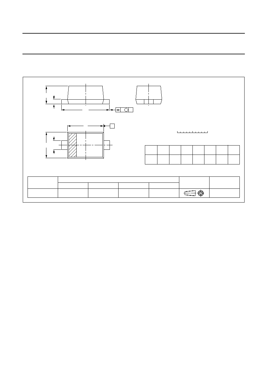
PACKAGE OUTLINE
REFERENCES
OUTLINE
VERSION
EUROPEAN
PROJECTION
ISSUE DATE
IEC
JEDEC
EIAJ
SOD523
SC-79
98-11-25
Plastic surface mounted package; 2 leads
SOD523
0
0.5
1 mm
scale
D
1
2
HE
E
bp
A
c
v
M
A
A
UNIT
bp
c
D
E
v
mm
0.35
0.25
0.2
0.1
0.15
0.9
0.7
1.3
1.1
A
0.7
0.5
HE
1.7
1.5
DIMENSIONS (mm are the original dimensions)
Note
1. The marking bar indicates the cathode.
(1)