 | ÐлекÑÑоннÑй компоненÑ: BAP64-06 | СкаÑаÑÑ:  PDF PDF  ZIP ZIP |
Äîêóìåíòàöèÿ è îïèñàíèÿ www.docs.chipfind.ru
DATA SHEET
Preliminary specification
1999 Dec 17
DISCRETE SEMICONDUCTORS
BAP64-06
Silicon PIN diode
ok, halfpage
M3D088
1999 Dec 17
2
Philips Semiconductors
Preliminary specification
Silicon PIN diode
BAP64-06
FEATURES
· High voltage, current controlled
· RF resistor for RF attenuators and switches
· Low diode capacitance
· Low diode forward resistance
· Low series inductance
· For applications up to 3 GHz.
APPLICATIONS
· RF attenuators and switches.
DESCRIPTION
Two planar PIN diodes in common anode configuration in
a SOT23 small plastic SMD package.
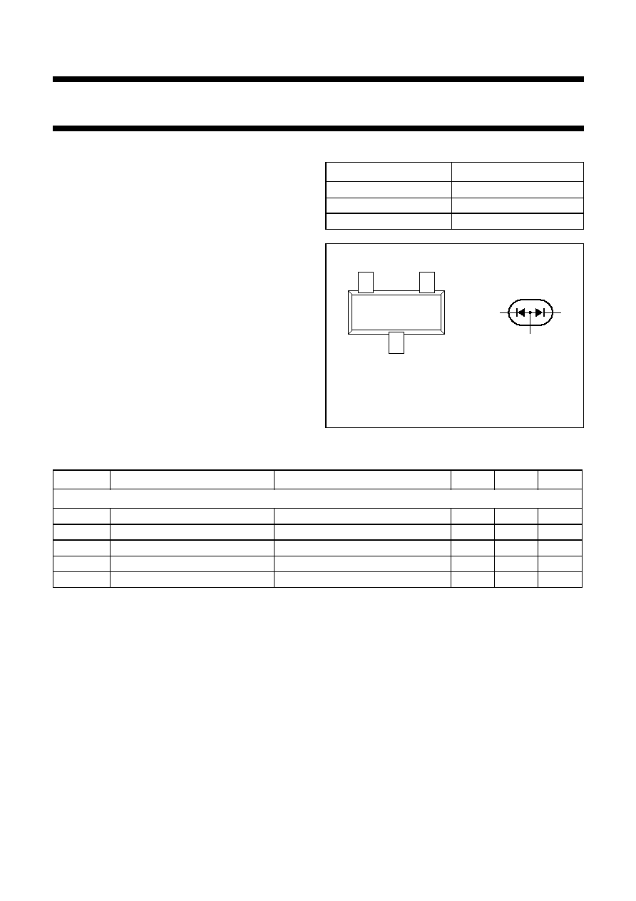
PINNING
PIN
DESCRIPTION
1
anode
2
cathode
3
common connection
ook, 4 columns
2
1
3
MAM206
Top view
2
1
3
Marking code: 6Kp
Fig.1 Simplified outline (SOT23) and symbol.
LIMITING VALUES
In accordance with the Absolute Maximum Rating System (IEC 134).
SYMBOL
PARAMETER
CONDITIONS
MIN.
MAX.
UNIT
Per diode
V
R
continuous reverse voltage
-
175
V
I
F
continuous forward current
-
100
mA
P
tot
total power dissipation
T
s
= 90
°C
-
250
mW
T
stg
storage temperature
-65
+150
°C
T
j
junction temperature
-65
+150
°C
1999 Dec 17
3
Philips Semiconductors
Preliminary specification
Silicon PIN diode
BAP64-06
ELECTRICAL CHARACTERISTICS
T
j
= 25
°C unless otherwise specified.
Note
1.
Guaranteed on AQL basis: inspection level S4, AQL 1.0.
THERMAL CHARACTERISTICS
SYMBOL
PARAMETER
CONDITIONS
TYP.
MAX.
UNIT
Per diode
V
F
forward voltage
I
F
= 50 mA
0.95
1.1
V
I
R
reverse current
V
R
= 175 V
-
10
µA
V
R
= 20 V
-
1
µA
C
d
diode capacitance
V
R
= 0; f = 1 MHz
0.52
-
pF
V
R
= 1 V; f = 1 MHz
0.37
-
pF
V
R
= 20 V; f = 1 MHz
0.23
0.35
pF
r
D
diode forward resistance
I
F
= 0.5 mA; f = 100 MHz; note 1
20
40
I
F
= 1 mA; f = 100 MHz; note 1
10
20
I
F
= 10 mA; f = 100 MHz; note 1
2
3.8
I
F
= 100 mA; f = 100 MHz; note 1
0.7
1.35
L
charge carrier life time
when switched from I
F
= 10 mA to
I
R
= 6 mA; R
L
= 100
;
measured at I
R
= 3 mA
1.55
-
µs
L
S
series inductance
1.4
-
nH
SYMBOL
PARAMETER
VALUE
UNIT
R
th j-s
thermal resistance from junction to soldering point
220
K/W
1999 Dec 17
4
Philips Semiconductors
Preliminary specification
Silicon PIN diode
BAP64-06
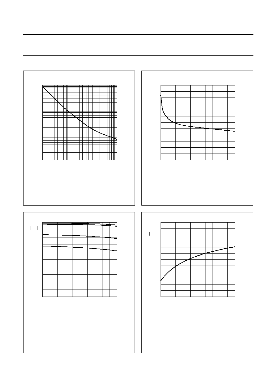
GRAPHICAL DATA
handbook, halfpage
10
2
10
1
10
-1
MCD777
10
-1
1
IF (mA)
rD
(
)
10
10
2
Fig.2
Forward resistance as a function of
forward current; typical values.
f = 100 MHz; T
j
= 25
°C.
handbook, halfpage
0
20
600
0
200
400
4
VR (V)
Cd
(fF)
12
8
16
MCD778
Fig.3
Diode capacitance as a function of reverse
voltage; typical values.
f = 1 MHz; T
j
= 25
°C.
handbook, halfpage
0.5
3
0
-5
S21
2
(dB)
-4
-3
-2
-1
1
f (GHz)
(1)
(2)
(3)
(4)
1.5
2
2.5
MCD779
Fig.4
Insertion loss (
|S
21
|
2
) of the diode as a
function of frequency; typical values.
(1) I
F
= 100 mA.
(2) I
F
= 10 mA.
(3) I
F
= 1 mA.
(4) I
F
= 0.5 mA.
Diode inserted in series with a 50
stripline circuit
and biased via the analyzer Tee network.
T
amb
= 25
°C.
handbook, halfpage
0.5
3
0
-30
-20
-10
1
f (GHz)
1.5
2
2.5
MCD780
S21
2
(dB)
Fig.5
Isolation (
|S
21
|
2
) of the diode as a function
of frequency; typical values.
Diode zero biased and inserted in series with a 50
stripline circuit.
T
amb
= 25
°C.
1999 Dec 17
5
Philips Semiconductors
Preliminary specification
Silicon PIN diode
BAP64-06
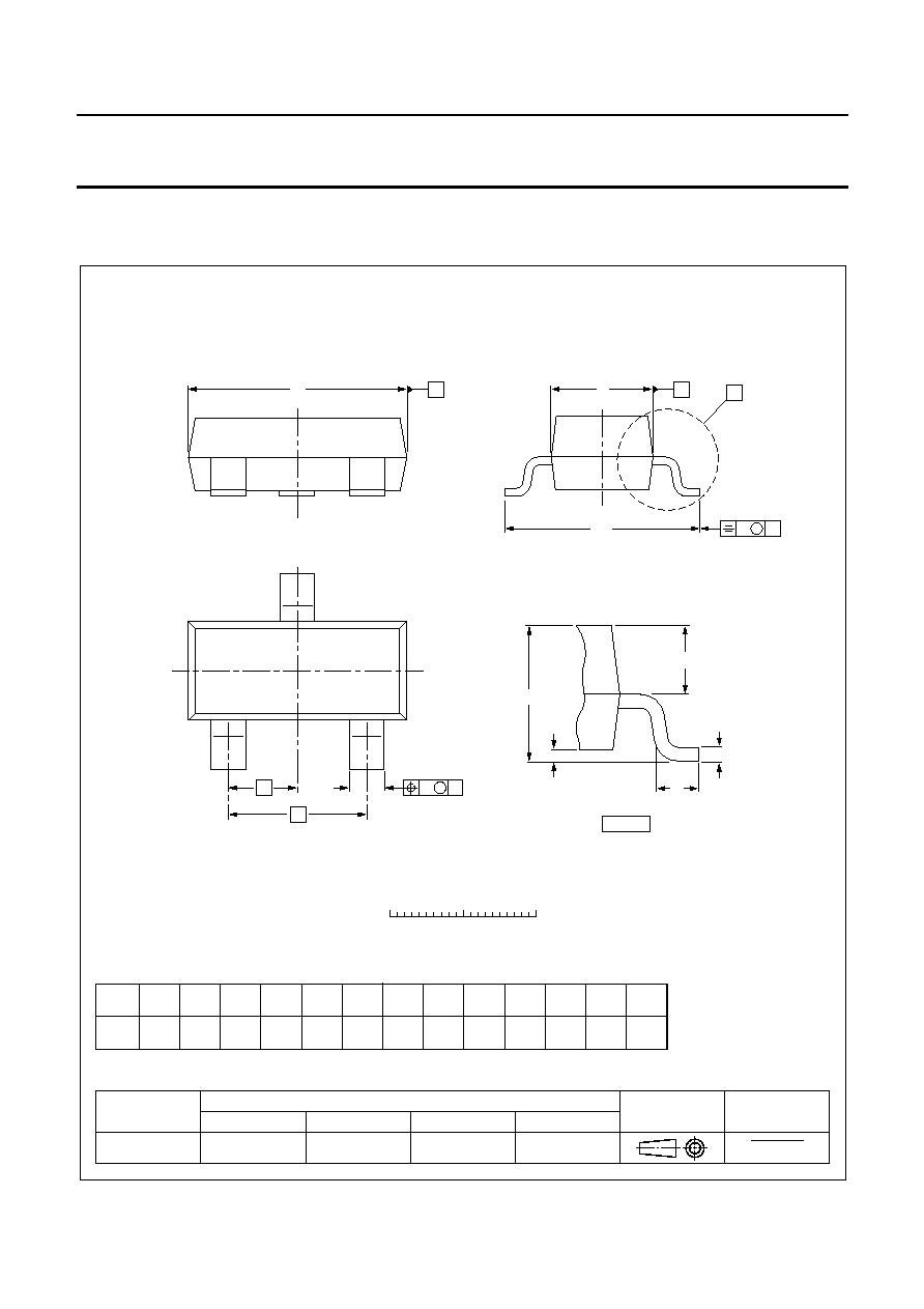
PACKAGE OUTLINE
UNIT
A
1
max.
b
p
c
D
E
e
1
H
E
L
p
Q
w
v
REFERENCES
OUTLINE
VERSION
EUROPEAN
PROJECTION
ISSUE DATE
97-02-28
99-09-13
IEC
JEDEC
EIAJ
mm
0.1
0.48
0.38
0.15
0.09
3.0
2.8
1.4
1.2
0.95
e
1.9
2.5
2.1
0.55
0.45
0.1
0.2
DIMENSIONS (mm are the original dimensions)
0.45
0.15
SOT23
TO-236AB
bp
D
e1
e
A
A1
Lp
Q
detail X
HE
E
w
M
v
M
A
B
A
B
0
1
2 mm
scale
A
1.1
0.9
c
X
1
2
3
Plastic surface mounted package; 3 leads
SOT23