2003 Aug 12
2
Philips Semiconductors
Product specification
High voltage switching diode
BAS521
FEATURES
∑
High switching speed: max. 50 ns
∑
High continuous reverse voltage: 300 V
∑
Repetitive peak forward current: 625 mA
∑
Ultra small plastic SMD package.
APPLICATIONS
∑
High speed switching
∑
High voltage switching.
DESCRIPTION
The BAS521 is a high-voltage switching diode fabricated
in planar technology and encapsulated in an ultra small
SOD523 (SC-79) plastic SMD package.
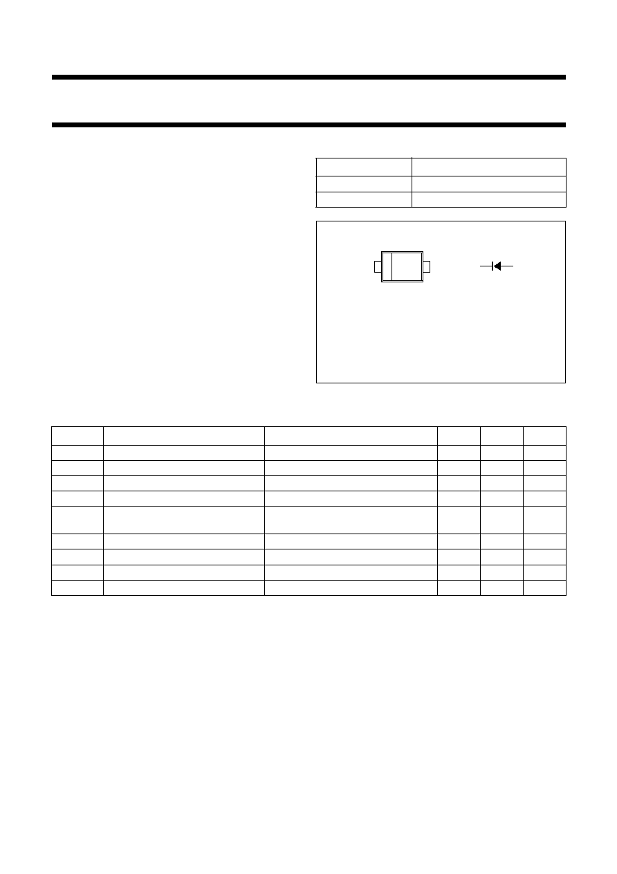
PINNING
PIN
DESCRIPTION
1
cathode
2
anode
handbook, halfpage
1
2
Top view
MAM408
Fig.1
Simplified outline (SOD523; SC-79), and
symbol.
Marking code: L4.
The marking bar indicates the cathode.
LIMITING VALUES
In accordance with the absolute Maximum Rating System (IEC 60134).
Note
1. T
s
is the temperature at the soldering point of the cathode tab.
SYMBOL
PARAMETER
CONDITIONS
MIN.
MAX.
UNIT
V
R
continuous reverse voltage
-
300
V
V
RRM
repetitive peak reverse voltage
-
300
V
I
F
continuous forward current
T
s
90
∞
C; note 1
-
250
mA
I
FRM
repetitive peak forward current
t
p
= 1 ms;
= 0.25
-
1
A
I
FSM
non-repetitive peak forward current
t
p
= 1
µ
s; square wave; T
j
= 25
∞
C
prior to surge
-
4.5
A
P
tot
total power dissipation
T
s
90
∞
C; note 1
-
500
mW
T
stg
storage temperature
-
65
+150
∞
C
T
j
junction temperature
-
150
∞
C
T
amb
operating ambient temperature
-
65
+150
∞
C

2003 Aug 12
3
Philips Semiconductors
Product specification
High voltage switching diode
BAS521
ELECTRICAL CHARACTERISTICS
T
amb
= 25
∞
C unless otherwise specified.
Note
1. Pulse test: t
p
= 300
µ
s;
= 0.02.
THERMAL CHARACTERISTICS
Notes
1. Soldering point of the cathode tab.
2. Refer to SOD523 (SC-79) standard mounting conditions.
SYMBOL
PARAMETER
CONDITIONS
MIN.
TYP.
MAX.
UNIT
V
BR
breakdown voltage
I
R
= 100
µ
A
300
340
-
V
V
F
forward voltage
I
F
= 100 mA; note 1
-
0.95
1.1
V
I
R
reverse current
V
R
= 250 V
-
30
150
nA
V
R
= 250 V; T
a
= 150
∞
C
-
40
100
µ
A
t
rr
reverse recovery time
when switched from I
F
= 30 mA to
I
R
= 30 mA; R
L
= 100
; measured at
I
R
= 3 mA
-
16
50
ns
C
d
diode capacitance
V
R
= 0 V; f = 1 MHz
-
0.4
5
pF
SYMBOL
PARAMETER
CONDITIONS
VALUE
UNIT
R
th j-s
thermal resistance from junction to solder point
note 1
120
K/W
R
th j-a
thermal resistance from junction to ambient
note 2
500
K/W
2003 Aug 12
4
Philips Semiconductors
Product specification
High voltage switching diode
BAS521
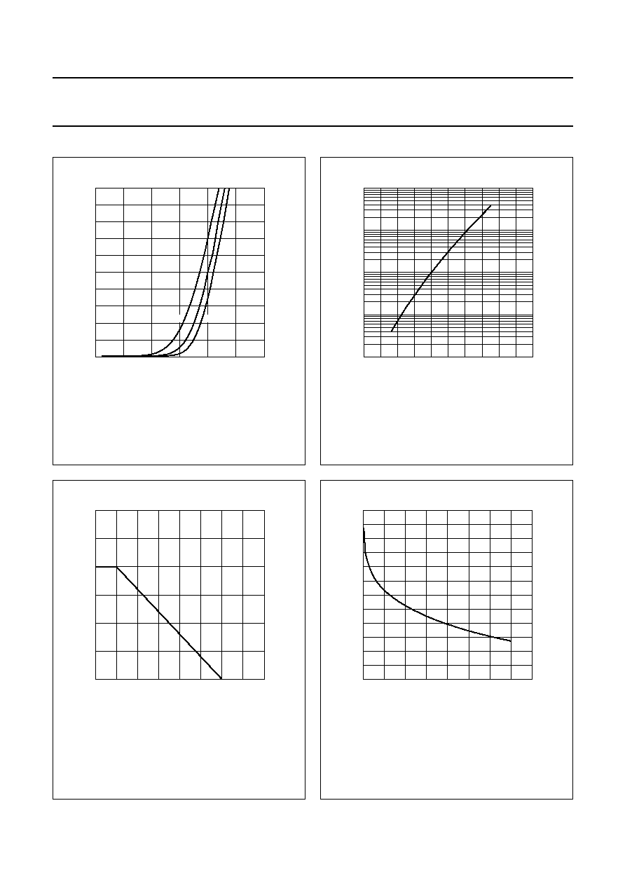
GRAPHICAL DATA
handbook, halfpage
0
0.5
1
(2)
1.5
IF
(mA)
VF (V)
500
0
400
300
200
100
MHC618
(1)
(3)
Fig.2
Forward current as a function of forward
voltage; typical values.
(1) T
amb
= 150
∞
C.
(2) T
amb
= 75
∞
C.
(3) T
amb
=25
∞
C.
handbook, halfpage
200
0
40
80
120
IR
(
µ
A)
160
Tj (
∞
C)
10
2
10
1
10
-
1
10
-
2
MHC619
Fig.3
Reverse current as a function of junction
temperature.
V
R
= V
Rmax
; typical values.
handbook, halfpage
0
300
200
100
0
50
100
200
Tamb (
∞
C)
150
IF
(mA)
MHC620
Fig.4
Maximum permissible continuous forward
current as a function of ambient
temperature.
handbook, halfpage
0
10
20
40
0.42
0.3
0.34
0.38
30
Cd
(pF)
VR (V)
MHC621
Fig.5
Diode capacitance as a function of reverse
voltage; typical values.

2003 Aug 12
5
Philips Semiconductors
Product specification
High voltage switching diode
BAS521
handbook, full pagewidth
MBG703
10
tp (
µ
s)
1
IFSM
(A)
10
2
10
-
1
10
4
10
2
10
3
10
1
Fig.6 Maximum permissible non-repetitive peak forward current as a function of pulse duration.
Based on square wave currents.
T
j
= 25
∞
C prior to surge.
