2002 Nov 18
2
Philips Semiconductors
Product specification
Low-voltage variable capacitance diodes
BB145B; BB145B-01
FEATURES
�
Ultra small plastic SMD package
�
C4: 2.75 pF; ratio: 2.4
�
Low series resistance.
APPLICATIONS
�
Voltage controlled oscillators
(VCO).
DESCRIPTION
The BB145B is a planar technology
variable capacitance diode in a
SOD523 (SC-79) package.
The BB145B-01 is a planar
technology variable capacitance
diode in a SOD723 package.
PINNING
PIN
DESCRIPTION
1
cathode
2
anode
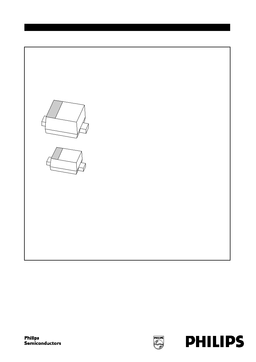
Fig.1 Simplified outline
(SOD523; SC-79) and symbol.
handbook, 2 columns
1
2
MBK441
Marking code: Z.
Orientation of marking code as shown.
Cathode side indicated by a bar.
Z
fpage
1
2
Top view
Z1
MCE159
Fig.2 Simplified outline
(SOD723) and symbol.
Marking code: Z1.
Orientation of marking code as shown.
Cathode side indicated by a bar.
LIMITING VALUES
In accordance with the Absolute Maximum Rating System (IEC 60134).
ELECTRICAL CHARACTERISTICS
T
j
= 25
�
C unless otherwise specified.
SYMBOL
PARAMETER
CONDITIONS
MIN.
MAX.
UNIT
V
R
continuous reverse voltage
-
6
V
V
RM
peak reverse voltage
in series with a 10 k
resistor
-
8
V
I
F
continuous forward current
-
20
mA
T
stg
storage temperature
-
55
+150
�
C
T
j
operating junction temperature
-
55
+150
�
C
SYMBOL
PARAMETER
CONDITIONS
MIN.
MAX.
UNIT
I
R
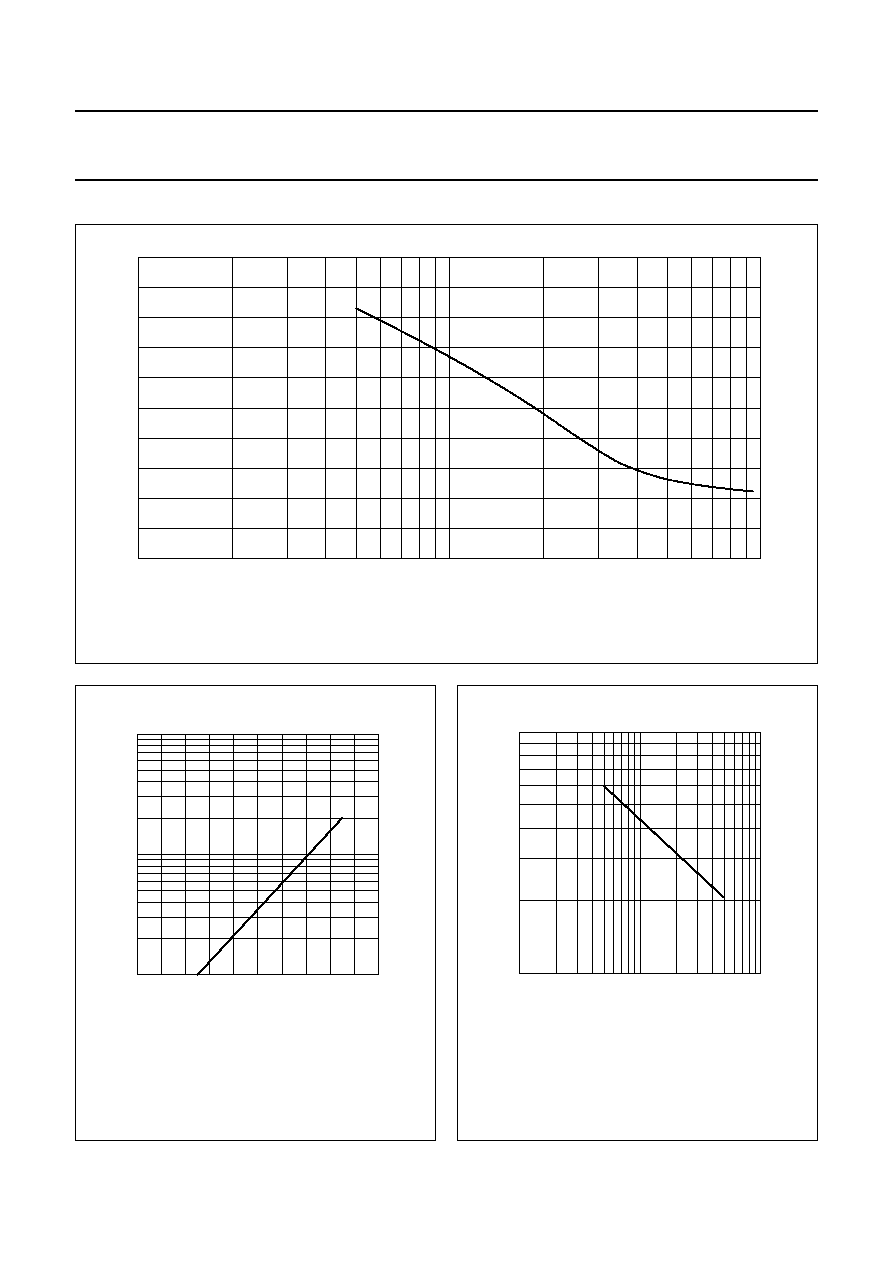
reverse current
V
R
= 6 V; see Fig.4
-
10
nA
V
R
= 6 V; T
j
= 85
�
C; see Fig.4
-
200
nA
r
s
diode series resistance
f = 470 MHz; V
R
= 1 V
-
0.6
C
d
diode capacitance
V
R
= 1 V; f = 1 MHz; see Figs 3 and 5
6.4
7.2
pF
V
R
= 4 V; f = 1 MHz; see Figs 3 and 5
2.55
2.95
pF
capacitance ratio
f = 1 MHz
2.2
-
CAUTION
This product is supplied in anti-static packing to prevent damage caused by electrostatic discharge during transport
and handling. For further information, refer to Philips specs.: SNW-EQ-608, SNW-FQ-302A and SNW-FQ-302B.
C
d 1V
(
)
C
d 4V
(
)
----------------
2002 Nov 18
4
Philips Semiconductors
Product specification
Low-voltage variable capacitance diodes
BB145B; BB145B-01
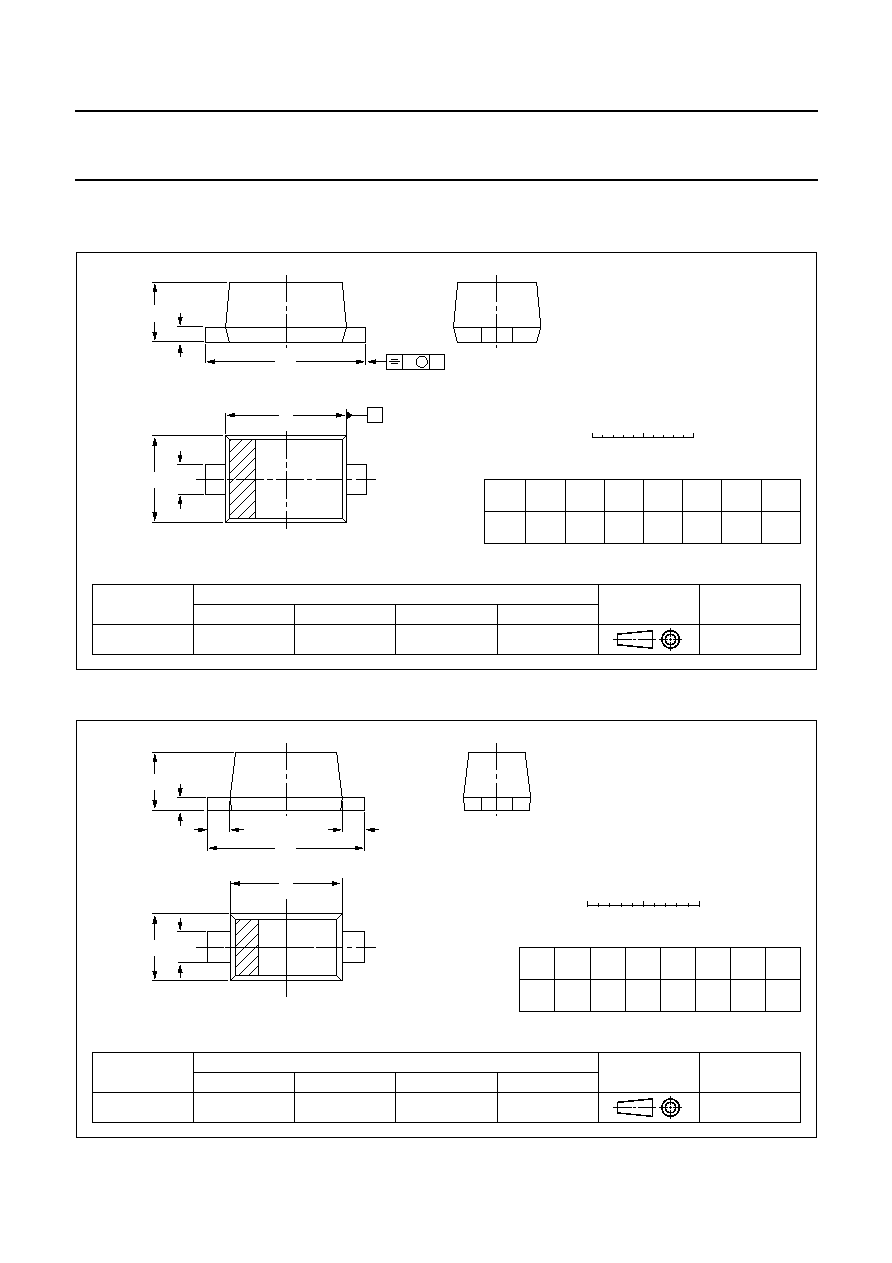
PACKAGE OUTLINE
REFERENCES
OUTLINE
VERSION
EUROPEAN
PROJECTION
ISSUE DATE
IEC
JEDEC
EIAJ
SOD523
SC-79
98-11-25
Plastic surface mounted package; 2 leads
SOD523
0
0.5
1 mm
scale
D
1
2
HE
E
bp
A
c
v
M
A
A
UNIT
bp
c
D
E
v
mm
0.35
0.25
0.2
0.1
0.15
0.9
0.7
1.3
1.1
A
0.7
0.5
HE
1.7
1.5
DIMENSIONS (mm are the original dimensions)
Note
1. The marking bar indicates the cathode.
(1)
REFERENCES
OUTLINE
VERSION
EUROPEAN
PROJECTION
ISSUE DATE
IEC
JEDEC
JEITA
SOD723
02-07-05
Plastic surface mounted package; 2 leads
SOD723
0
0.5
1 mm
scale
D
1
2
HE
Lp
Lp
E
bp
A
c
UNIT
bp
c
D
E
mm
0.32
0.25
0.15
0.08
0.65
0.55
1.05
0.95
A
0.55
0.49
HE
1.45
1.35
Lp
0.27
0.13
DIMENSIONS (mm are the original dimensions)
Note
1. The marking bar indicates the cathode.
(1)

2002 Nov 18
5
Philips Semiconductors
Product specification
Low-voltage variable capacitance diodes
BB145B; BB145B-01
DATA SHEET STATUS
Notes
1. Please consult the most recently issued data sheet before initiating or completing a design.
2. The product status of the device(s) described in this data sheet may have changed since this data sheet was
published. The latest information is available on the Internet at URL http://www.semiconductors.philips.com.
3. For data sheets describing multiple type numbers, the highest-level product status determines the data sheet status.
LEVEL
DATA SHEET
STATUS
(1)
PRODUCT
STATUS
(2)(3)
DEFINITION
I
Objective data
Development
This data sheet contains data from the objective specification for product
development. Philips Semiconductors reserves the right to change the
specification in any manner without notice.
II
Preliminary data Qualification
This data sheet contains data from the preliminary specification.
Supplementary data will be published at a later date. Philips
Semiconductors reserves the right to change the specification without
notice, in order to improve the design and supply the best possible
product.
III
Product data
Production
This data sheet contains data from the product specification. Philips
Semiconductors reserves the right to make changes at any time in order
to improve the design, manufacturing and supply. Relevant changes will
be communicated via a Customer Product/Process Change Notification
(CPCN).
DEFINITIONS
Short-form specification
The data in a short-form
specification is extracted from a full data sheet with the
same type number and title. For detailed information see
the relevant data sheet or data handbook.
Limiting values definition
Limiting values given are in
accordance with the Absolute Maximum Rating System
(IEC 60134). Stress above one or more of the limiting
values may cause permanent damage to the device.
These are stress ratings only and operation of the device
at these or at any other conditions above those given in the
Characteristics sections of the specification is not implied.
Exposure to limiting values for extended periods may
affect device reliability.
Application information
Applications that are
described herein for any of these products are for
illustrative purposes only. Philips Semiconductors make
no representation or warranty that such applications will be
suitable for the specified use without further testing or
modification.
DISCLAIMERS
Life support applications
These products are not
designed for use in life support appliances, devices, or
systems where malfunction of these products can
reasonably be expected to result in personal injury. Philips
Semiconductors customers using or selling these products
for use in such applications do so at their own risk and
agree to fully indemnify Philips Semiconductors for any
damages resulting from such application.
Right to make changes
Philips Semiconductors
reserves the right to make changes in the products -
including circuits, standard cells, and/or software -
described or contained herein in order to improve design
and/or performance. When the product is in full production
(status `Production'), relevant changes will be
communicated via a Customer Product/Process Change
Notification (CPCN). Philips Semiconductors assumes no
responsibility or liability for the use of any of these
products, conveys no licence or title under any patent,
copyright, or mask work right to these products, and
makes no representations or warranties that these
products are free from patent, copyright, or mask work
right infringement, unless otherwise specified.