 | –≠–ª–µ–∫—Ç—Ä–æ–Ω–Ω—ã–π –∫–æ–º–ø–æ–Ω–µ–Ω—Ç: BBZA420A | –°–∫–∞—á–∞—Ç—å:  PDF PDF  ZIP ZIP |
Document Outline
- FEATURES
- APPLICATIONS
- DESCRIPTION
- PINNING
- LIMITING VALUES
- THERMAL CHARACTERISTICS
- ELECTRICAL CHARACTERISTICS
- APPLICATION INFORMATION
- Typical common anode application
- Device placement and printed-circuit board layout
- PACKAGE OUTLINE
- DEFINITIONS
- LIFE SUPPORT APPLICATIONS
DATA SHEET
Product specification
Supersedes data of 1998 Oct 30
1999 May 20
DISCRETE SEMICONDUCTORS
BZA420A
Quadruple ESD transient voltage
suppressor
book, halfpage
M3D302
1999 May 20
2
Philips Semiconductors
Product specification
Quadruple ESD transient voltage suppressor
BZA420A
FEATURES
∑
ESD rating >8 kV, according to IEC1000-4-2
∑
SOT457 surface mount package
∑
Common anode configuration
∑
Non-clamping range
-
0.5 to 20 V
∑
Maximum reverse peak power dissipation:
19.6 W at t
p
= 1 ms
∑
Maximum clamping voltage at peak pulse current:
28 V at I
ZSM
= 0.7 A.
APPLICATIONS
∑
Computers and peripherals
∑
Audio and video equipment
∑
Communication systems
∑
Medical equipment.
DESCRIPTION
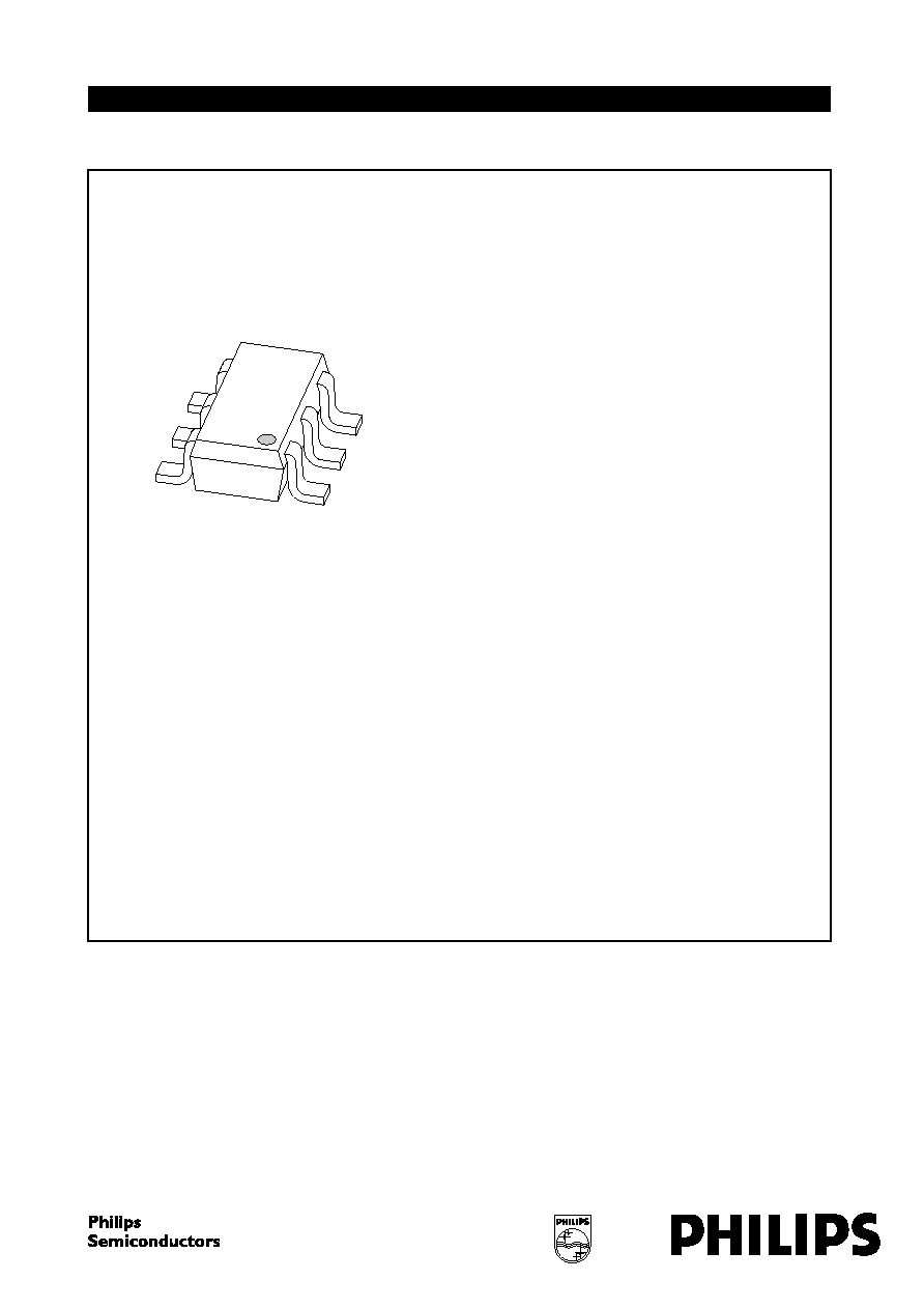
Monolithic transient voltage suppressor diode in a six lead
SOT457 (SC-74) package for 4-bit wide ESD transient
suppression at 20 V level.
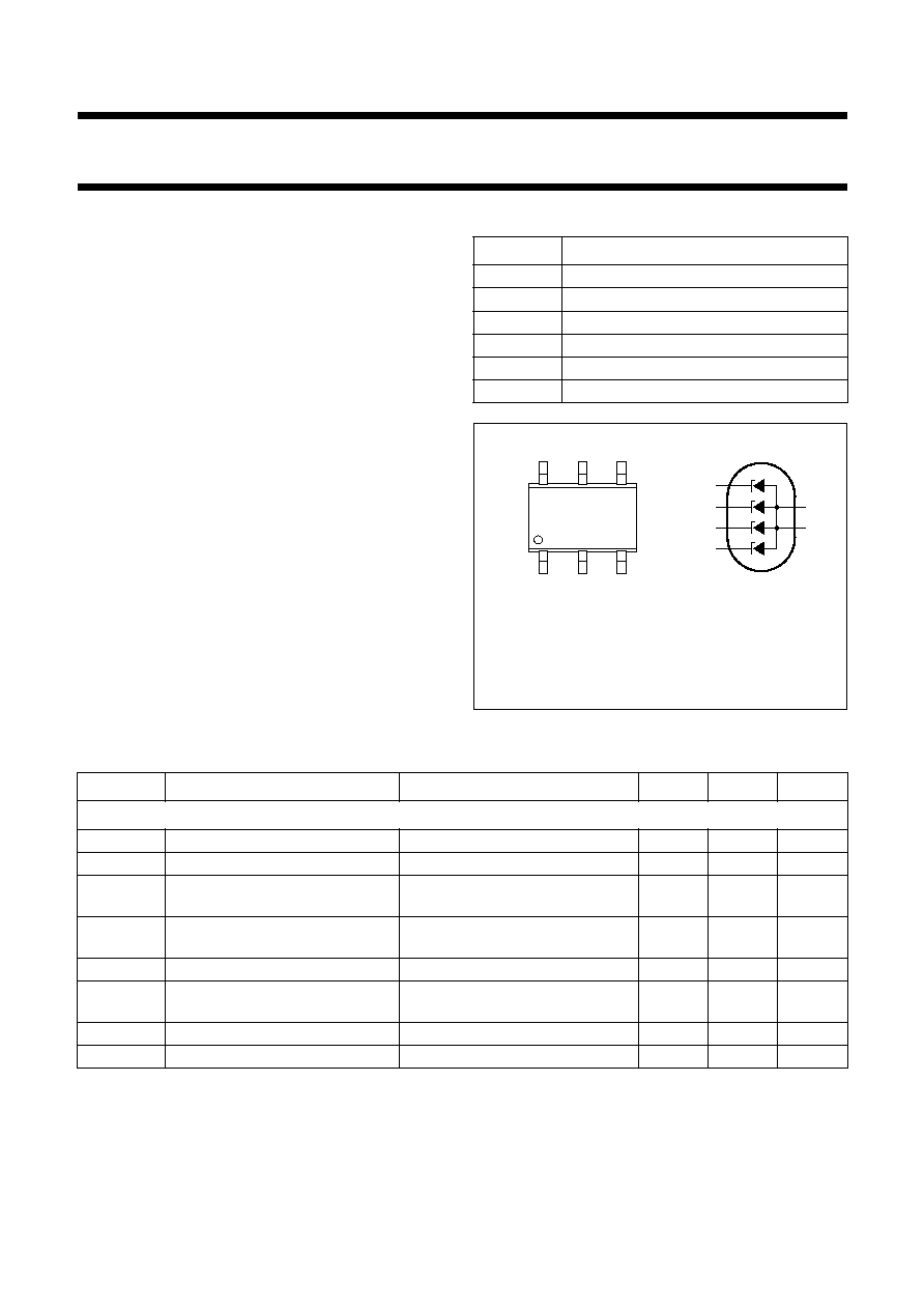
PINNING
PIN
DESCRIPTION
1
cathode 1
2
common
3
cathode 2
4
cathode 3
5
common
6
cathode 4
Fig.1 Simplified outline (SOT457) and symbol.
handbook, halfpage
1
3
2
4
5
6
1
3
4
6
2
5
Top view
MAM357
Marking code: Z0.
LIMITING VALUES
In accordance with the Absolute Maximum Rating System (IEC 134).
Notes
1. T
s
is the temperature at the soldering point of the anode pin.
2. DC working current limited by P
tot max
.
SYMBOL
PARAMETER
CONDITIONS
MIN.
MAX.
UNIT
Per diode
I
Z
working current
T
s
= 60
∞
C; note 1
-
note 2
mA
I
F
continuous forward current
T
s
= 60
∞
C
-
100
mA
I
FSM
non-repetitive peak forward
current
t
p
= 1 ms; square pulse
-
3.75
A
I
ZSM
non-repetitive peak reverse
current
t
p
= 1 ms; square pulse; see Fig.2
-
0.7
A
P
tot
total power dissipation
T
s
= 60
∞
C; see Fig.3
-
720
mW
P
ZSM
non repetitive peak reverse power
dissipation
square pulse; t
p
= 1 ms; see Fig.4
-
19.6
W
T
stg
storage temperature
-
65
+150
∞
C
T
j
junction temperature
-
65
+150
∞
C

1999 May 20
3
Philips Semiconductors
Product specification
Quadruple ESD transient voltage suppressor
BZA420A
THERMAL CHARACTERISTICS
ELECTRICAL CHARACTERISTICS
T
j
= 25
∞
C unless otherwise specified.
SYMBOL
PARAMETER
CONDITIONS
VALUE
UNIT
R
th j-s
thermal resistance from junction to soldering point
one or more diodes loaded
125
K/W
SYMBOL
PARAMETER
CONDITIONS
MIN.
TYP.
MAX.
UNIT
Per diode
V
Z
working voltage
I
Z
= 1 mA
19
20
21
V
V
F
forward voltage
I
F
= 200 mA
-
-
1.3
V
V
ZSM
non-repetitive peak reverse voltage I
ZSM
= 0.7 A; t
p
= 1 ms
-
-
28
V
I
R
reverse current
V
R
= 15 V
-
-
100
nA
r
dif
differential resistance
I
Z
= 1 mA
-
-
125
S
Z
temperature coefficient of working
voltage
I
Z
= 5 mA
-
16.2
-
mV/K
C
d
diode capacitance
see Fig.5
V
R
= 0; f = 1 MHz
-
-
48
pF
V
R
= 15 V; f = 1 MHz
-
-
14
pF
1999 May 20
4
Philips Semiconductors
Product specification
Quadruple ESD transient voltage suppressor
BZA420A
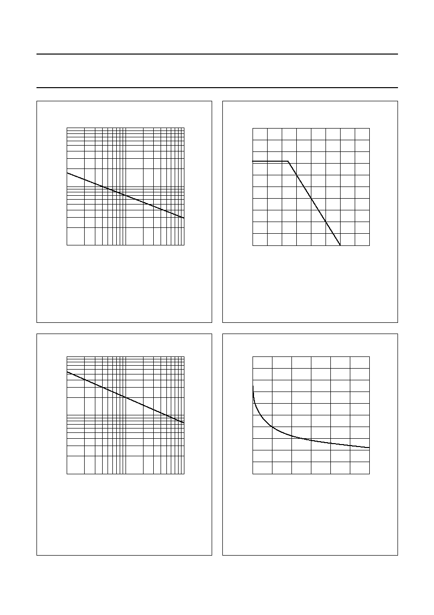
Fig.2
Maximum non-repetitive peak reverse
current as a function of pulse time.
handbook, halfpage
10
1
10
-
1
IZSM
(A)
tp (ms)
MDA197
10
-
1
1
10
Fig.3 Power derating curve.
All diodes loaded.
handbook, halfpage
0
50
100
200
1000
0
Ptot
(mW)
Ts (
o
C)
800
150
600
400
200
MDA198
Fig.4
Maximum non-repetitive peak reverse
power dissipation as a function of pulse
duration (square pulse).
P
ZSM
= V
ZSM
◊
I
ZSM
.
V
ZSM
is the non-repetitive peak reverse voltage at I
ZSM
.
handbook, halfpage
10
2
10
1
PZSM
(W)
tp (ms)
MDA199
10
-
1
1
10
Fig.5
Diode capacitance as a function of reverse
voltage; typical values.
T
j
= 25
∞
C; f = 1 MHz.
handbook, halfpage
0
5
10
VR (V)
15
50
0
Cd
(pF)
40
30
20
10
MDA200
1999 May 20
5
Philips Semiconductors
Product specification
Quadruple ESD transient voltage suppressor
BZA420A
Fig.6 ESD clamping test set-up and waveforms.
handbook, full pagewidth
MBK386
450
50
Note 1: attenuator is only used for open
socket high voltage measurements
IEC 1000-4-2 network
CZ = 150 pF; RZ = 330
1/4 BZA420A
RG 223/U
50
coax
RZ
CZ
ESD TESTER
DIGITIZING
OSCILLOSCOPE
10
◊
ATTENUATOR
note 1
GND
unclamped
+
1 kV ESD voltage waveform
(IEC 1000
-
4
-
2 network)
clamped
+
1 kV ESD voltage waveform
(IEC 1000
-
4
-
2 network)
unclamped
-
1 kV ESD voltage waveform
(IEC 1000
-
4
-
2 network)
clamped
-
1 kV ESD voltage waveform
(IEC 1000
-
4
-
2 network)
GND
GND
GND
vertical scale = 100 V/Div
horizontal scale = 50 ns/Div
vertical scale = 10 V/Div
horizontal scale = 50 ns/Div
vertical scale = 100 V/Div
horizontal scale = 50 ns/Div
vertical scale = 10 V/Div
horizontal scale = 50 ns/Div