1999 Apr 15
2
Philips Semiconductors
Product specification
NPN general purpose transistor
BC817W
FEATURES
∑
High current (max. 500 mA)
∑
Low voltage (max. 45 V).
APPLICATIONS
∑
General purpose switching and amplification.
DESCRIPTION
NPN transistor in a SOT323 plastic package.
PNP complement: BC807W.
MARKING
Note
1.
= - : Made in Hong Kong.
= t : Made in Malaysia.
TYPE
NUMBER
MARKING
CODE
(1)
TYPE
NUMBER
MARKING
CODE
(1)
BC817W
6D
BC818W
6H
BC817-16W
6A
BC818-16W
6E
BC817-25W
6B
BC818-25W
6F
BC817-40W
6C
BC818-40W
6G
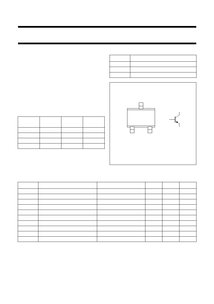
PINNING
PIN
DESCRIPTION
1
base
2
emitter
3
collector
Fig.1
Simplified outline (SOT323) and symbol.
handbook, halfpage
2
3
1
MAM062
3
2
1
Top view
LIMITING VALUES
In accordance with the Absolute Maximum Rating System (IEC 134).
Note
1. Transistor mounted on an FR4 printed-circuit board.
SYMBOL
PARAMETER
CONDITIONS
MIN.
MAX.
UNIT
V
CBO
collector-base voltage
open emitter
-
50
V
V
CEO
collector-emitter voltage
open base; I
C
= 10 mA
-
45
V
V
EBO
emitter-base voltage
open collector
-
5
V
I
C
collector current (DC)
-
500
mA
I
CM
peak collector current
-
1
A
I
BM
peak base current
-
200
mA
P
tot
total power dissipation
T
amb
25
∞
C; note 1
-
200
mW
T
stg
storage temperature
-
65
+150
∞
C
T
j
junction temperature
-
150
∞
C
T
amb
operating ambient temperature
-
65
+150
∞
C
1999 Apr 15
3
Philips Semiconductors
Product specification
NPN general purpose transistor
BC817W
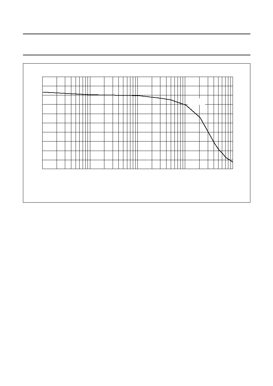
THERMAL CHARACTERISTICS
Note
1. Transistor mounted on an FR4 printed-circuit board.
CHARACTERISTICS
T
amb
= 25
∞
C unless otherwise specified.
Note
1. Pulse test: t
p
300
µ
s;
0.02.
SYMBOL
PARAMETER
CONDITIONS
VALUE
UNIT
R
th j-a
thermal resistance from junction to ambient
note 1
625
K/W
SYMBOL
PARAMETER
CONDITIONS
MIN.
MAX.
UNIT
I
CBO
collector cut-off current
I
E
= 0; V
CB
= 20 V
-
100
nA
I
E
= 0; V
CB
= 20 V; T
j
= 150
∞
C
-
5
µ
A
I
EBO
emitter cut-off current
I
C
= 0; V
EB
= 5 V
-
100
nA
h
FE
DC current gain
I
C
= 100 mA; V
CE
= 1 V; note 1;
see Figs 2, 3 and 4
BC817W
100
600
BC817-16W
100
250
BC817-25W
160
400
BC817-40W
250
600
DC current gain
I
C
= 500 mA; V
CE
= 1 V; note 1
40
-
V
CEsat
collector-emitter saturation
voltage
I
C
= 500 mA; I
B
= 50 mA; note 1
-
700
mV
V
BE
base-emitter voltage
I
C
= 500 mA; V
CE
= 1 V; note 1
-
1.2
mV
C
c
collector capacitance
I
E
= i
e
= 0; V
CB
= 10 V; f = 1 MHz
-
5
pF
f
T
transition frequency
I
C
= 10 mA; V
CE
= 5 V; f = 100 MHz
100
-
MHz

1999 Apr 15
4
Philips Semiconductors
Product specification
NPN general purpose transistor
BC817W
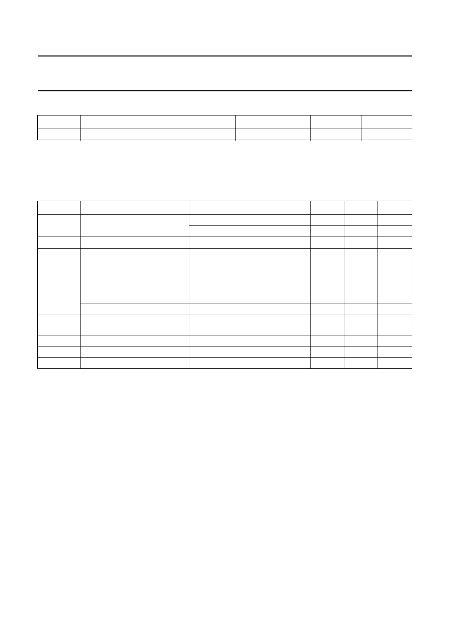
Fig.2 DC current gain; typical values.
BC817-16W.
handbook, full pagewidth
0
20
40
80
120
160
MBH721
10
-
1
1
hFE
10
IC (mA)
10
2
10
3
VCE = 1 V
Fig.3 DC current gain; typical values.
BC817-25W.
handbook, full pagewidth
0
500
100
200
300
400
MBH720
10
-
1
1
hFE
10
IC (mA)
10
2
10
3
VCE = 1 V