 | –≠–ª–µ–∫—Ç—Ä–æ–Ω–Ω—ã–π –∫–æ–º–ø–æ–Ω–µ–Ω—Ç: BCV63BTR2 | –°–∫–∞—á–∞—Ç—å:  PDF PDF  ZIP ZIP |
Document Outline
- FEATURES
- APPLICATIONS
- DESCRIPTION
- PINNING
- MARKING
- LIMITING VALUES
- THERMAL CHARACTERISTICS
- CHARACTERISTICS
- APPLICATION INFORMATION
- PACKAGE OUTLINE
- DEFINITIONS
DATA SHEET
Product specification
Supersedes data of 1997 Mar 10
1999 May 21
DISCRETE SEMICONDUCTORS
BCV63; BCV63B
NPN general purpose double
transistors
M3D071
1999 May 21
2
Philips Semiconductors
Product specification
NPN general purpose double transistors
BCV63; BCV63B
FEATURES
∑
Low current (max. 100 mA)
∑
Low voltage (max. 30 and 6 V).
APPLICATIONS
∑
General purpose switching and amplification
∑
For use in Schmitt-trigger applications.
DESCRIPTION
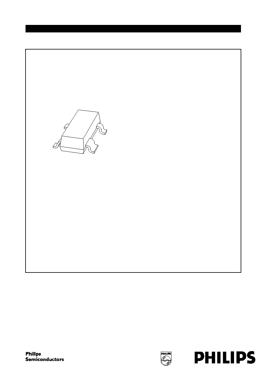
NPN double transistor in a SOT143B plastic package.
PNP complement: BCV64B.
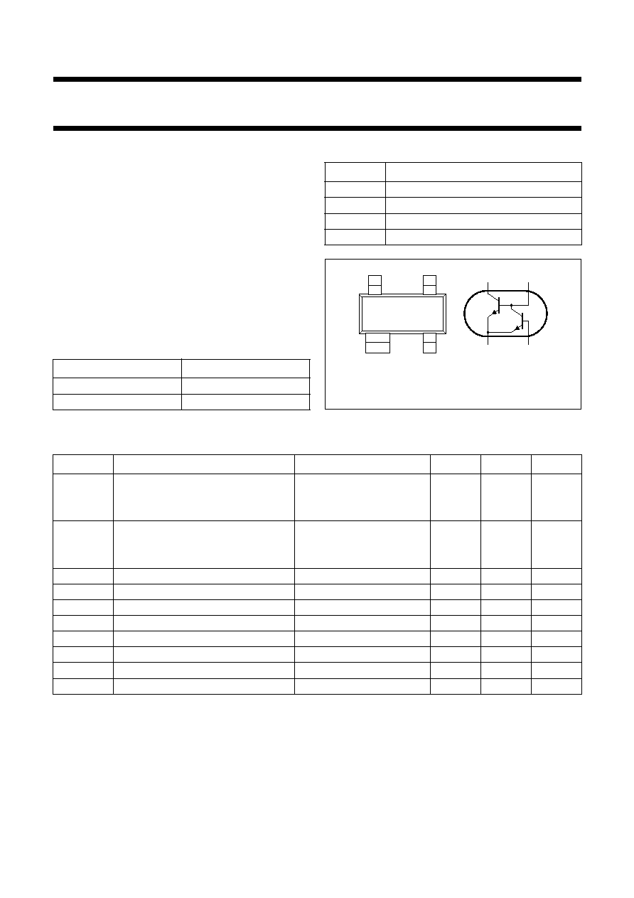
PINNING
PIN
DESCRIPTION
1
collector TR2 and base TR1
2
collector TR1
3
emitter TR1 and TR2
4
base TR2
Fig.1 Simplified outline (SOT143B) and symbol.
handbook, halfpage
4
1
2
3
MAM316
Top view
2
1
3
4
TR2
TR1
MARKING
TYPE NUMBER
MARKING CODE
BCV63
D95
BCV63B
D96
LIMITING VALUES
In accordance with the Absolute Maximum Rating System (IEC 134).
Note
1. Transistor mounted on a printed-circuit board.
SYMBOL
PARAMETER
CONDITIONS
MIN.
MAX.
UNIT
V
CBO
collector-base voltage
open emitter
TR1
-
30
V
TR2
-
6
V
V
CEO
collector-emitter voltage
open base
TR1
-
30
V
TR2
-
6
V
V
EBO
emitter-base voltage
open collector
-
6
V
I
C
collector current (DC)
-
100
mA
I
CM
peak collector current
-
200
mA
I
B
base current (DC)
-
100
mA
P
tot
total power dissipation
T
amb
25
∞
C; note 1
-
250
mW
T
stg
storage temperature
-
65
+150
∞
C
T
j
junction temperature
-
150
∞
C
T
amb
operating ambient temperature
-
65
+150
∞
C

1999 May 21
3
Philips Semiconductors
Product specification
NPN general purpose double transistors
BCV63; BCV63B
THERMAL CHARACTERISTICS
Note
1. Transistor mounted on a printed-circuit board.
CHARACTERISTICS
T
amb
= 25
∞
C unless otherwise specified.
Notes
1. Group selection will be done on TR1. Due to matched dies, h
FE
values for TR2 are the same as for TR1.
2. V
BEsat
decreases by approximately 1.7 mV/K with increasing temperature.
3. V
BE
decreases by approximately 2 mV/K with increasing temperature.
SYMBOL
PARAMETER
CONDITIONS
VALUE
UNIT
R
th j-a
thermal resistance from junction to ambient
note 1
500
K/W
SYMBOL
PARAMETER
CONDITIONS
MIN.
TYP.
MAX.
UNIT
I
CBO
collector cut-off current
I
E
= 0; V
CB
= 30 V
-
-
15
nA
I
E
= 0; V
CB
= 30 V; T
j
= 150
∞
C
-
-
5
µ
A
h
FE
DC current gain
BCV63 TR1
I
C
= 2 mA; V
CE
= 5 V
110
-
800
BCV63 TR2
I
C
= 2 mA; V
CE
= 700 mV; note 1
110
-
800
BCV63B TR1
I
C
= 2 mA; V
CE
= 5 V
200
-
450
BCV63B TR2
I
C
= 2 mA; V
CE
= 700 mV; note 1
200
-
450
V
CEsat
collector-emitter saturation voltage I
C
= 10 mA; I
B
= 0.5 mA
-
75
300
mV
collector-emitter saturation voltage I
C
= 100 mA; I
B
= 5 mA
TR1
-
250
650
mV
TR2
-
250
-
mV
V
BEsat
base-emitter saturation voltage
I
C
= 10 mA; I
B
= 0.5 mA; note 2
-
700
-
mV
base-emitter saturation voltage
I
C
= 100 mA; I
B
= 5 mA; note 2
TR1
-
-
850
-
mV
V
BE
base-emitter voltage
TR1
I
C
= 2 mA; V
CE
= 5 V; note 3
600
650
750
mV
TR1
I
C
= 10 mA; V
CE
= 5 V; note 3
-
-
820
mV
TR2
I
C
= 2 mA; V
CE
= 700 mV; note 3
-
700
-
mV
C
c
collector capacitance
I
E
= i
e
= 0; V
CB
= 10 V; f = 1 MHz
TR1
-
4
-
pF
f
T
transition frequency
I
C
= 10 mA; V
CE
= 5 V; f = 100 MHz
TR1
100
-
-
MHz
1999 May 21
4
Philips Semiconductors
Product specification
NPN general purpose double transistors
BCV63; BCV63B
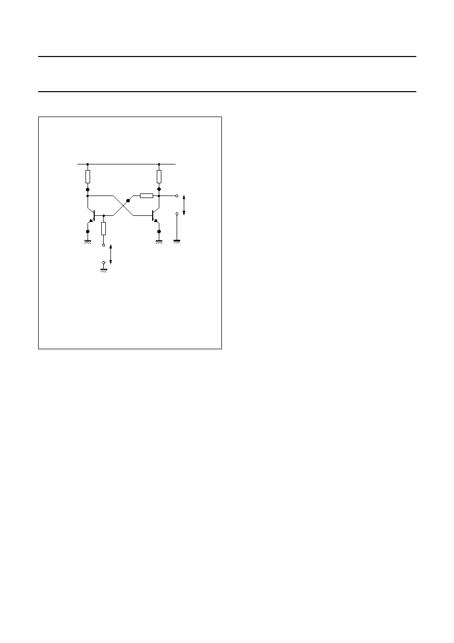
APPLICATION INFORMATION
Fig.2 Schmitt-trigger application.
handbook, halfpage
Rc
Rc
Vi
1
2
4
3
3
TR2
TR1
R2
R1
MGD829
Vo
1999 May 21
5
Philips Semiconductors
Product specification
NPN general purpose double transistors
BCV63; BCV63B
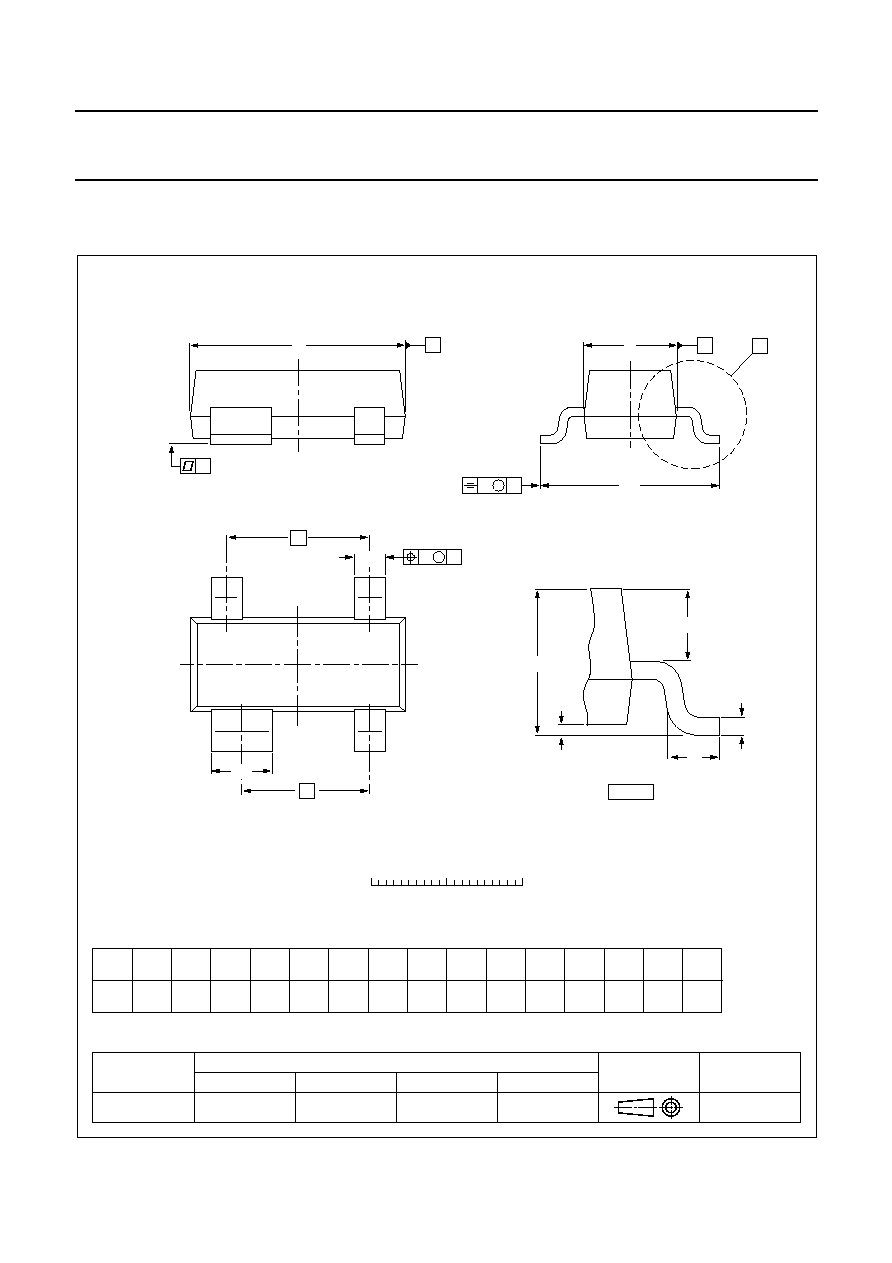
PACKAGE OUTLINE
UNIT
A
REFERENCES
OUTLINE
VERSION
EUROPEAN
PROJECTION
ISSUE DATE
IEC
JEDEC
EIAJ
mm
1.1
0.9
A1
max
0.1
b1
0.88
0.78
c
0.15
0.09
D
3.0
2.8
E
1.4
1.2
HE
y
w
v
Q
2.5
2.1
0.45
0.15
0.55
0.45
e
1.9
e1
1.7
Lp
0.1
0.1
0.2
bp
0.48
0.38
DIMENSIONS (mm are the original dimensions)
SOT143B
97-02-28
0
1
2 mm
scale
Plastic surface mounted package; 4 leads
SOT143B
D
HE
E
A
B
v
M
A
X
A
A1
Lp
Q
detail X
c
y
w
M
e1
e
B
2
1
3
4
b1
bp