1999 Apr 19
2
Philips Semiconductors
Product specification
NPN medium power transistors
BCX54; BCX55; BCX56
FEATURES
∑
High current (max. 1 A)
∑
Low voltage (max. 80 V).
APPLICATIONS
∑
Driver stages of audio and video amplifiers.
DESCRIPTION
NPN medium power transistor in a SOT89 plastic
package. PNP complements: BCX51, BCX52 and BCX53.
MARKING
TYPE
NUMBER
MARKING
CODE
TYPE
NUMBER
MARKING
CODE
BCX54
BA
BCX55-16
BM
BCX54-10
BC
BCX56
BH
BCX54-16
BD
BCX56-10
BK
BCX55
BE
BCX56-16
BL
BCX55-10
BG
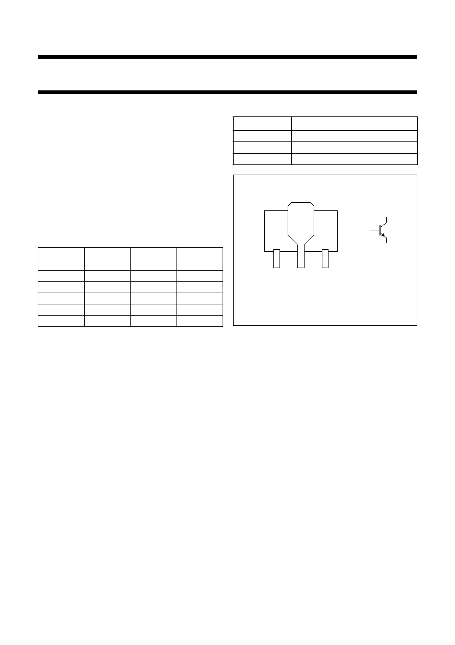
PINNING
PIN
DESCRIPTION
1
emitter
2
collector
3
base
Fig.1 Simplified outline (SOT89) and symbol.
handbook, halfpage
1
2
3
Bottom view
MAM296
3
2
1

1999 Apr 19
3
Philips Semiconductors
Product specification
NPN medium power transistors
BCX54; BCX55; BCX56
LIMITING VALUES
In accordance with the Absolute Maximum Rating System (IEC 134).
Note
1. Device mounted on a printed-circuit board, single sided copper, tinplated, mounting pad for collector 6 cm
2
.
For other mounting conditions, see
"Thermal considerations for SOT89 in the General Part of associated Handbook".
THERMAL CHARACTERISTICS
Note
1. Device mounted on a printed-circuit board, single sided copper, tinplated, mounting pad for collector 6 cm
2
.
For other mounting conditions, see
"Thermal considerations for SOT89 in the General Part of associated Handbook".
SYMBOL
PARAMETER
CONDITIONS
MIN.
MAX.
UNIT
V
CBO
collector-base voltage
open emitter
BCX54
-
45
V
BCX55
-
60
V
BCX56
-
100
V
V
CEO
collector-emitter voltage
open base
BCX54
-
45
V
BCX55
-
60
V
BCX56
-
80
V
V
EBO
emitter-base voltage
open collector
-
5
V
I
C
collector current (DC)
-
1
A
I
CM
peak collector current
-
1.5
A
I
BM
peak base current
-
0.2
A
P
tot
total power dissipation
T
amb
25
∞
C; note 1
-
1.3
W
T
stg
storage temperature
-
65
+150
∞
C
T
j
junction temperature
-
150
∞
C
T
amb
operating ambient temperature
-
65
+150
∞
C
SYMBOL
PARAMETER
CONDITIONS
VALUE
UNIT
R
th j-a
thermal resistance from junction to ambient
note 1
94
K/W
R
th j-s
thermal resistance from junction to soldering point
14
K/W
1999 Apr 19
4
Philips Semiconductors
Product specification
NPN medium power transistors
BCX54; BCX55; BCX56
CHARACTERISTICS
T
amb
= 25
∞
C unless otherwise specified.
SYMBOL
PARAMETER
CONDITIONS
MIN.
TYP.
MAX.
UNIT
I
CBO
collector cut-off current
I
E
= 0; V
CB
= 30 V
-
-
100
nA
I
E
= 0; V
CB
= 30 V; T
j
= 125
∞
C
-
-
10
µ
A
I
EBO
emitter cut-off current
I
C
= 0; V
EB
= 5 V
-
-
100
nA
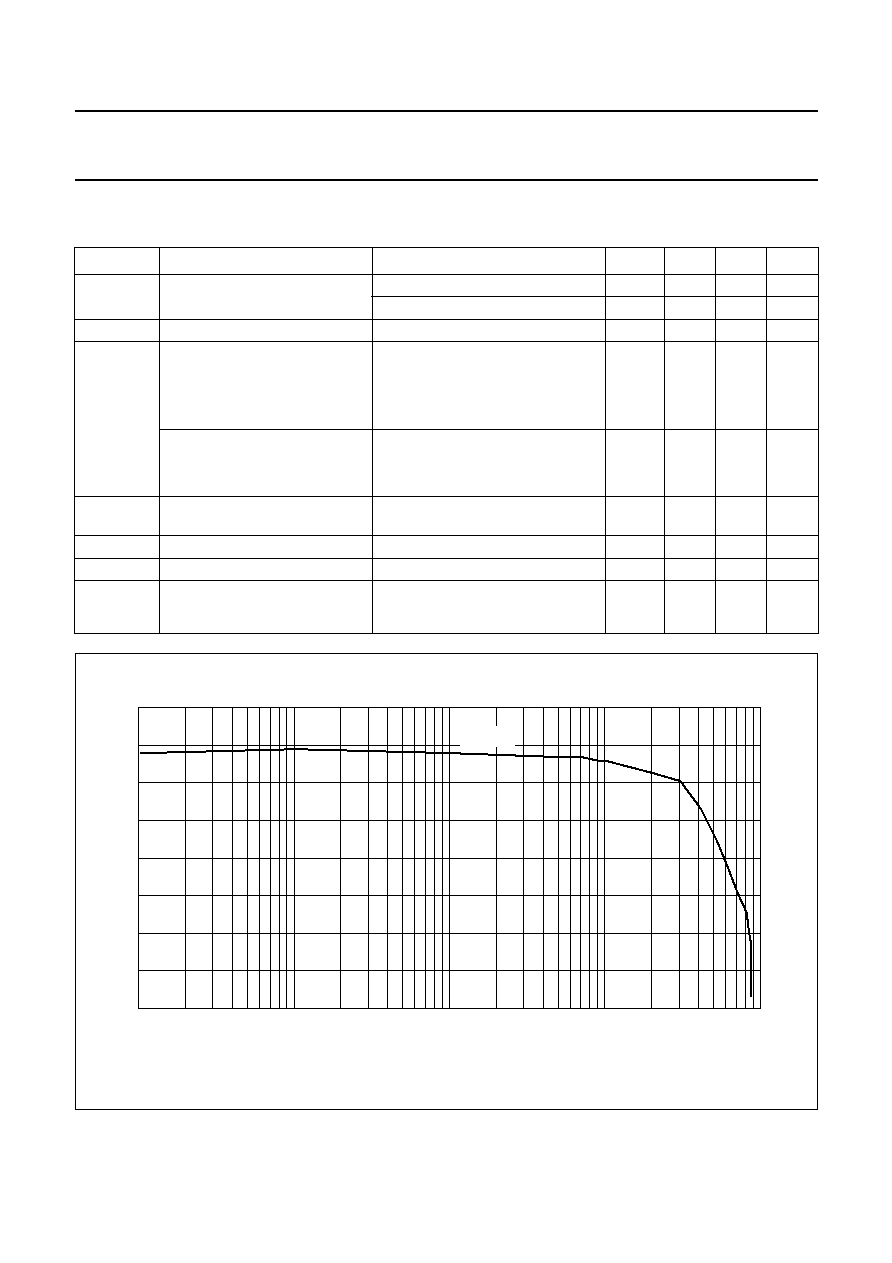
h
FE
DC current gain
V
CE
= 2 V; (see Fig.2)
I
C
= 5 mA
40
-
-
I
C
= 150 mA
63
-
250
I
C
= 500 mA
25
-
-
DC current gain
I
C
= 150 mA; V
CE
= 2 V; (see Fig.2)
BCX54-10; 55-10; 56-10
63
-
160
BCX54-16; 55-16; 56-16
100
-
250
V
CEsat
collector-emitter saturation
voltage
I
C
= 500 mA; I
B
= 50 mA
-
-
0.5
V
V
BE
base-emitter voltage
I
C
= 500 mA; V
CE
= 2 V
-
-
1
V
f
T
transition frequency
I
C
= 10 mA; V
CE
= 5 V; f = 100 MHz
-
130
-
MHz
DC current gain ratio of the
complementary pairs
I
C
= 150 mA;
V
CE
= 2 V
-
1.3
1.6
h
FE1
h
FE2
-----------
Fig.2 DC current gain; typical values.
handbook, full pagewidth
0
160
80
120
40
MBH729
10
-
1
hFE
1
IC (mA)
10
10
3
10
2
VCE = 2 V
1999 Apr 19
5
Philips Semiconductors
Product specification
NPN medium power transistors
BCX54; BCX55; BCX56
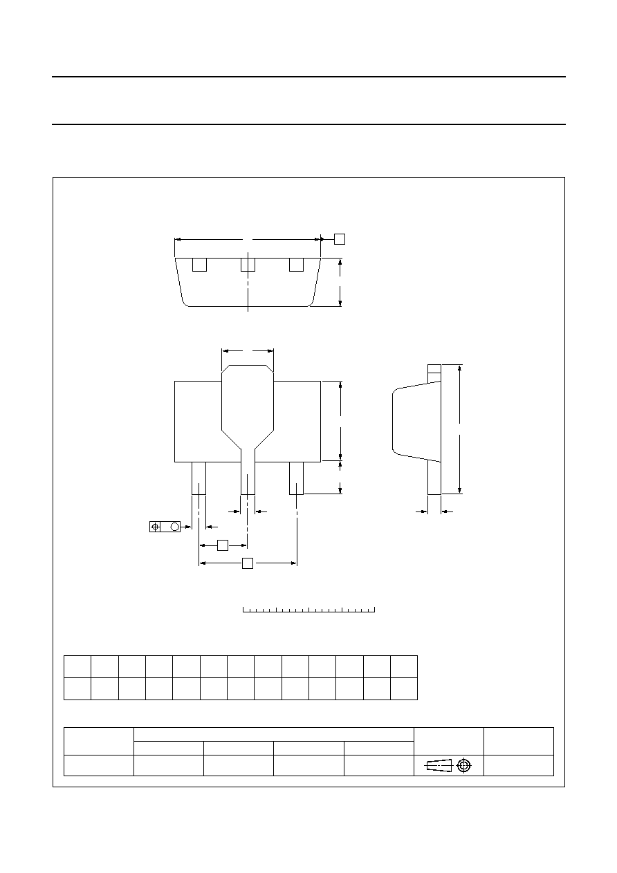
PACKAGE OUTLINE
REFERENCES
OUTLINE
VERSION
EUROPEAN
PROJECTION
ISSUE DATE
IEC
JEDEC
EIAJ
DIMENSIONS (mm are the original dimensions)
SOT89
97-02-28
w
M
e
1
e
E
HE
B
0
2
4 mm
scale
b3
b2
b1
c
D
L
A
Plastic surface mounted package; collector pad for good heat transfer; 3 leads
SOT89
1
2
3
UNIT
A
mm
1.6
1.4
0.48
0.35
c
0.44
0.37
D
4.6
4.4
E
2.6
2.4
HE
4.25
3.75
e
3.0
w
0.13
e1
1.5
L
min.
0.8
b2
b1
0.53
0.40
b3
1.8
1.4