 | –≠–ª–µ–∫—Ç—Ä–æ–Ω–Ω—ã–π –∫–æ–º–ø–æ–Ω–µ–Ω—Ç: BCY79 | –°–∫–∞—á–∞—Ç—å:  PDF PDF  ZIP ZIP |
Document Outline
- FEATURES
- APPLICATIONS
- DESCRIPTION
- PINNING
- QUICK REFERENCE DATA
- LIMITING VALUES
- THERMAL CHARACTERISTICS
- CHARACTERISTICS
- PACKAGE OUTLINE
- DEFINITIONS
- LIFE SUPPORT APPLICATIONS
DATA SHEET
Product specification
Supersedes data of September 1994
File under Discrete Semiconductors, SC04
1997 Jun 18
DISCRETE SEMICONDUCTORS
BCY78; BCY79
PNP switching transistors
M3D125
1997 Jun 18
2
Philips Semiconductors
Product specification
PNP switching transistors
BCY78; BCY79
FEATURES
∑
Low current (max. 100 mA)
∑
Low voltage (max. 45 V).
APPLICATIONS
∑
Switching and amplification.
DESCRIPTION
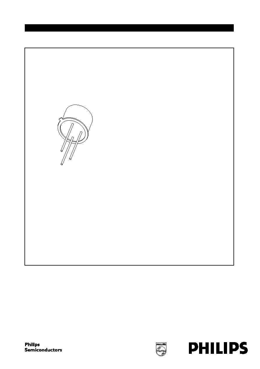
PNP switching transistor in a TO-18 metal package.
NPN complements: BCY58 and BCY59.
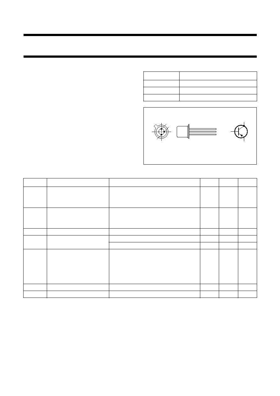
PINNING
PIN
DESCRIPTION
1
emitter
2
base
3
collector, connected to case
Fig.1 Simplified outline (TO-18) and symbol.
handbook, halfpage
MAM263
1
3
2
3
1
2
QUICK REFERENCE DATA
SYMBOL
PARAMETER
CONDITIONS
MIN.
MAX.
UNIT
V
CBO
collector-base voltage
open emitter
BCY78
-
-
32
V
BCY79
-
-
45
V
V
CEO
collector-emitter voltage
open base
BCY78
-
-
32
V
BCY79
-
-
45
V
I
C
collector current (DC)
-
-
100
mA
P
tot
total power dissipation
T
amb
45
∞
C
-
340
mW
T
case
45
∞
C
-
1
W
h
FE
DC current gain
I
C
=
-
2 mA; V
CE
=
-
5 V
BCY78/VII; BCY79/VII
120
220
BCY78/VIII; BCY79/VIII
180
310
BCY78/IX; BCY79/IX
250
460
BCY78/X
380
630
f
T
transition frequency
I
C
=
-
10 mA; V
CE
=
-
5 V
100
-
MHz
t
off
turn-off time
I
Con
=
-
100 mA; I
Bon
=
-
10 mA; I
Boff
= 10 mA
-
400
ns

1997 Jun 18
3
Philips Semiconductors
Product specification
PNP switching transistors
BCY78; BCY79
LIMITING VALUES
In accordance with the Absolute Maximum Rating System (IEC 134).
THERMAL CHARACTERISTICS
SYMBOL
PARAMETER
CONDITIONS
MIN.
MAX.
UNIT
V
CBO
collector-base voltage
open emitter
BCY78
-
-
32
V
BCY79
-
-
45
V
V
CEO
collector-emitter voltage
open base
BCY78
-
-
32
V
BCY79
-
-
45
V
V
EBO
emitter-base voltage
open collector
-
5
V
I
C
collector current (DC)
-
-
100
mA
I
CM
peak collector current
-
-
200
mA
I
BM
peak base current
-
-
200
mA
P
tot
total power dissipation
T
amb
45
∞
C
-
340
mW
T
case
45
∞
C
-
1
W
T
stg
storage temperature
-
65
+150
∞
C
T
j
junction temperature
-
200
∞
C
T
amb
operating ambient temperature
-
65
+150
∞
C
SYMBOL
PARAMETER
CONDITIONS
VALUE
UNIT
R
th j-a
thermal resistance from junction to ambient
in free air
450
K/W
R
th j-c
thermal resistance from junction to case
150
K/W

1997 Jun 18
4
Philips Semiconductors
Product specification
PNP switching transistors
BCY78; BCY79
CHARACTERISTICS
T
amb
= 25
∞
C unless otherwise specified.
SYMBOL
PARAMETER
CONDITIONS
MIN.
TYP.
MAX.
UNIT
I
CBO
collector cut-off current
BCY78
I
E
= 0; V
CB
=
-
32 V
-
-
2
-
15
nA
I
E
= 0; V
CB
=
-
32 V; T
amb
= 150
∞
C
-
-
-
10
µ
A
I
CBO
collector cut-off current
BCY79
I
E
= 0; V
CB
=
-
45 V
-
-
2
-
15
nA
I
E
= 0; V
CB
=
-
45 V; T
amb
= 150
∞
C
-
-
-
10
µ
A
I
EBO
emitter cut-off current
I
C
= 0; V
EB
=
-
5 V
-
-
-
20
nA
h
FE
DC current gain
I
C
=
-
10
µ
A; V
CE
=
-
5 V
BCY78/VII; BCY79/VII
-
140
-
BCY78/VIII; BCY79/VIII
30
200
-
BCY78/IX; BCY79/IX
40
270
-
BCY78/X
100
340
-
h
FE
DC current gain
I
C
=
-
2 mA; V
CE
=
-
5 V
BCY78/VII; BCY79/VII
120
170
220
BCY78/VIII; BCY79/VIII
180
250
310
BCY78/IX; BCY79/IX
250
350
460
BCY78/X
380
500
630
h
FE
DC current gain
I
C
=
-
10 mA; V
CE
=
-
1 V
BCY78/VII; BCY79/VII
80
180
-
BCY78/VIII; BCY79/VIII
120
260
400
BCY78/IX; BCY79/IX
160
360
630
BCY78/X
240
500
1000
h
FE
DC current gain
I
C
=
-
100 mA; V
CE
=
-
1 V
BCY78/VII; BCY79/VII
40
-
-
BCY78/VIII; BCY79/VIII
45
-
-
BCY78/IX; BCY79/IX
60
-
-
BCY78/X
60
-
-
V
CEsat
collector-emitter saturation voltage I
C
=
-
10 mA; I
B
=
-
250
µ
A
-
-
120
-
250
mV
I
C
=
-
100 mA; I
B
=
-
2.5 mA
-
-
400
-
800
mV
V
BEsat
base-emitter saturation voltage
I
C
=
-
10 mA; I
B
=
-
250
µ
A
-
600
-
700
-
850
mV
I
C
=
-
100 mA; I
B
=
-
2.5 mA
-
700
-
850
-
1200 mV
V
BE
base-emitter voltage
I
C
=
-
10
µ
A; V
CE
=
-
5 V
-
-
550
-
mV
I
C
=
-
2 mA; V
CE
=
-
5 V
-
600
-
650
-
750
mV
I
C
=
-
10 mA; V
CE
=
-
1 V
-
-
650
-
mV
I
C
=
-
100 mA; V
CE
=
-
1 V
-
-
750
-
mV
C
c
collector capacitance
I
E
= i
e
= 0; V
CB
=
-
10 V; f = 1 MHz
-
-
7
pF
C
e
emitter capacitance
I
C
= i
c
= 0; V
EB
=
-
500 mV; f = 1 MHz
-
-
15
pF
f
T
transition frequency
I
C
=
-
10 mA; V
CE
=
-
5 V; f = 100 MHz 100
-
-
MHz
1997 Jun 18
5
Philips Semiconductors
Product specification
PNP switching transistors
BCY78; BCY79
F
noise figure
I
C
=
-
200
µ
A; V
CE
=
-
5 V; R
S
= 2 k
;
f = 1 kHz; B = 200 Hz
-
-
10
dB
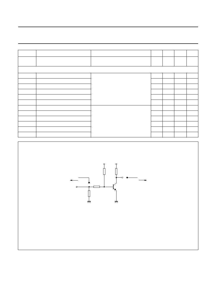
Switching times (between 10% and 90% levels); see Fig.2
t
on
turn-on time
I
Con
=
-
10 mA; I
Bon
=
-
1 mA;
I
Boff
= 1 mA; test conditions A
-
-
100
ns
t
d
delay time
-
-
50
ns
t
r
rise time
-
-
50
ns
t
off
turn-off time
-
-
700
ns
t
s
storage time
-
-
600
ns
t
f
fall time
-
-
100
ns
t
on
turn-on time
I
Con
=
-
100 mA; I
Bon
=
-
10 mA;
I
Boff
= 10 mA; test conditions B
-
-
100
ns
t
d
delay time
-
-
35
ns
t
r
rise time
-
-
65
ns
t
off
turn-off time
-
-
400
ns
t
s
storage time
-
-
300
ns
t
f
fall time
-
-
100
ns
SYMBOL
PARAMETER
CONDITIONS
MIN.
TYP.
MAX.
UNIT
Test conditions A
V
i
=
-
5 V; T = 500
µ
s; t
p
= 10
µ
s; t
r
= t
f
3 ns.
R1 = 56
; R2 = 2.5 k
; R
B
= 3.9 k
; R
C
= 270
.
V
BB
= 1.9 V; V
CC
=
-
3 V
Oscilloscope input impedance Z
i
= 50
.
Fig.2 Test circuit for switching times.
ndbook, full pagewidth
RC
R2
R1
DUT
MGD624
Vo
RB
(probe)
450
(probe)
450
oscilloscope
oscilloscope
VBB
Vi
VCC
Test conditions B
V
i
=
-
9.8 V; T = 500
µ
s; t
p
= 10
µ
s; t
r
= t
f
3 ns.
R1 = 62
; R2 = 470
; R
B
= 470
; R
C
= 100
.
V
BB
= 3.4 V; V
CC
=
-
10.8 V
Oscilloscope input impedance Z
i
= 50
.