 | –≠–ª–µ–∫—Ç—Ä–æ–Ω–Ω—ã–π –∫–æ–º–ø–æ–Ω–µ–Ω—Ç: BDP32 | –°–∫–∞—á–∞—Ç—å:  PDF PDF  ZIP ZIP |
DATA SHEET
Product specification
Supersedes data of 1997 Mar 10
1999 Apr 23
DISCRETE SEMICONDUCTORS
BDP32
PNP medium power transistor
handbook, halfpage
M3D087
1999 Apr 23
2
Philips Semiconductors
Product specification
PNP medium power transistor
BDP32
FEATURES
∑
High current (max. 3 A)
∑
Low voltage (max. 45 V).
APPLICATIONS
∑
General purpose medium power applications.
DESCRIPTION
PNP medium power transistor in a SOT223 plastic
package. NPN complement: BDP31.
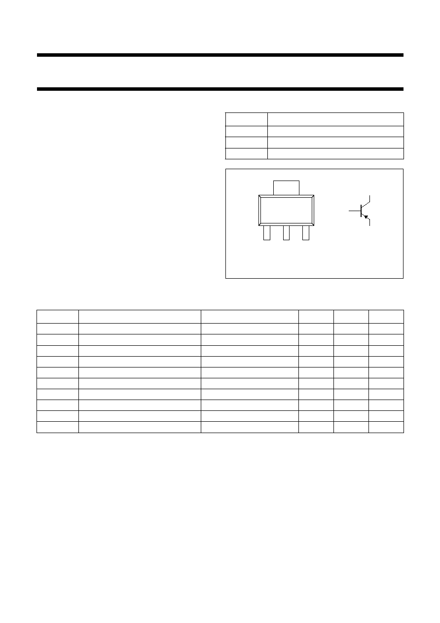
PINNING
PIN
DESCRIPTION
1
base
2,4
collector
3
emitter
Fig.1 Simplified outline (SOT223) and symbol.
handbook, halfpage
4
1
2
3
MAM288
Top view
3
2, 4
1
LIMITING VALUES
In accordance with the Absolute Maximum Rating System (IEC 134).
Note
1. Device mounted on a printed-circuit board, single sided copper, tinplated, mounting pad for collector 1 cm
2
.
For other mounting conditions, see
"Thermal considerations for the SOT223 in the General Part of associated
Handbook".
SYMBOL
PARAMETER
CONDITIONS
MIN.
MAX.
UNIT
V
CBO
collector-base voltage
open emitter
-
-
45
V
V
CEO
collector-emitter voltage
open base
-
-
45
V
V
EBO
emitter-base voltage
open collector
-
-
5
V
I
C
collector current (DC)
-
-
3
A
I
CM
peak collector current
-
-
6
A
I
BM
peak base current
-
-
0.5
A
P
tot
total power dissipation
T
amb
25
∞
C; note 1
-
1.35
W
T
stg
storage temperature
-
65
+150
∞
C
T
j
junction temperature
-
150
∞
C
T
amb
operating ambient temperature
-
65
+150
∞
C

1999 Apr 23
3
Philips Semiconductors
Product specification
PNP medium power transistor
BDP32
THERMAL CHARACTERISTICS
Note
1. Device mounted on a printed-circuit board, single sided copper, tinplated, mounting pad for collector 1 cm
2
.
For other mounting conditions, see
"Thermal considerations for the SOT223 in the General Part of associated
Handbook".
CHARACTERISTICS
T
amb
= 25
∞
C unless otherwise specified.
Note
1. Pulse test: t
p
300
µ
s;
0.02.
SYMBOL
PARAMETER
CONDITIONS
VALUE
UNIT
R
th j-a
thermal resistance from junction to ambient
note 1
91
K/W
R
th j-s
thermal resistance from junction to soldering point
10
K/W
SYMBOL
PARAMETER
CONDITIONS
MIN.
MAX.
UNIT
I
CBO
collector cut-off current
I
E
= 0; V
CB
=
-
40 V
-
-
50
nA
I
E
= 0; V
CB
=
-
40 V; T
j
= 150
∞
C
-
-
10
µ
A
I
EBO
emitter cut-off current
I
C
= 0; V
EB
=
-
5 V
-
-
50
nA
h
FE
DC current gain
I
C
=
-
0.5 A; V
CE
=
-
12 V; note 1; see Fig.2
40
-
I
C
=
-
2 A; V
CE
=
-
1 V; note 1; see Fig.2
20
-
V
CEsat
collector-emitter saturation
voltage
I
C
=
-
500 mA; I
B
=
-
50 mA; note 1
-
-
300
mV
I
C
=
-
2 A; I
B
=
-
200 mA; note 1
-
-
700
mV
V
BEsat
base-emitter saturation voltage
I
C
=
-
500 mA; I
B
=
-
50 mA; note 1
-
-
1.2
V
I
C
=
-
2 A; I
B
=
-
200 mA; note 1
-
-
1.5
V
f
T
transition frequency
V
CE
=
-
5 V; I
C
=
-
250 mA; f = 100 MHz
60
-
MHz
1999 Apr 23
4
Philips Semiconductors
Product specification
PNP medium power transistor
BDP32
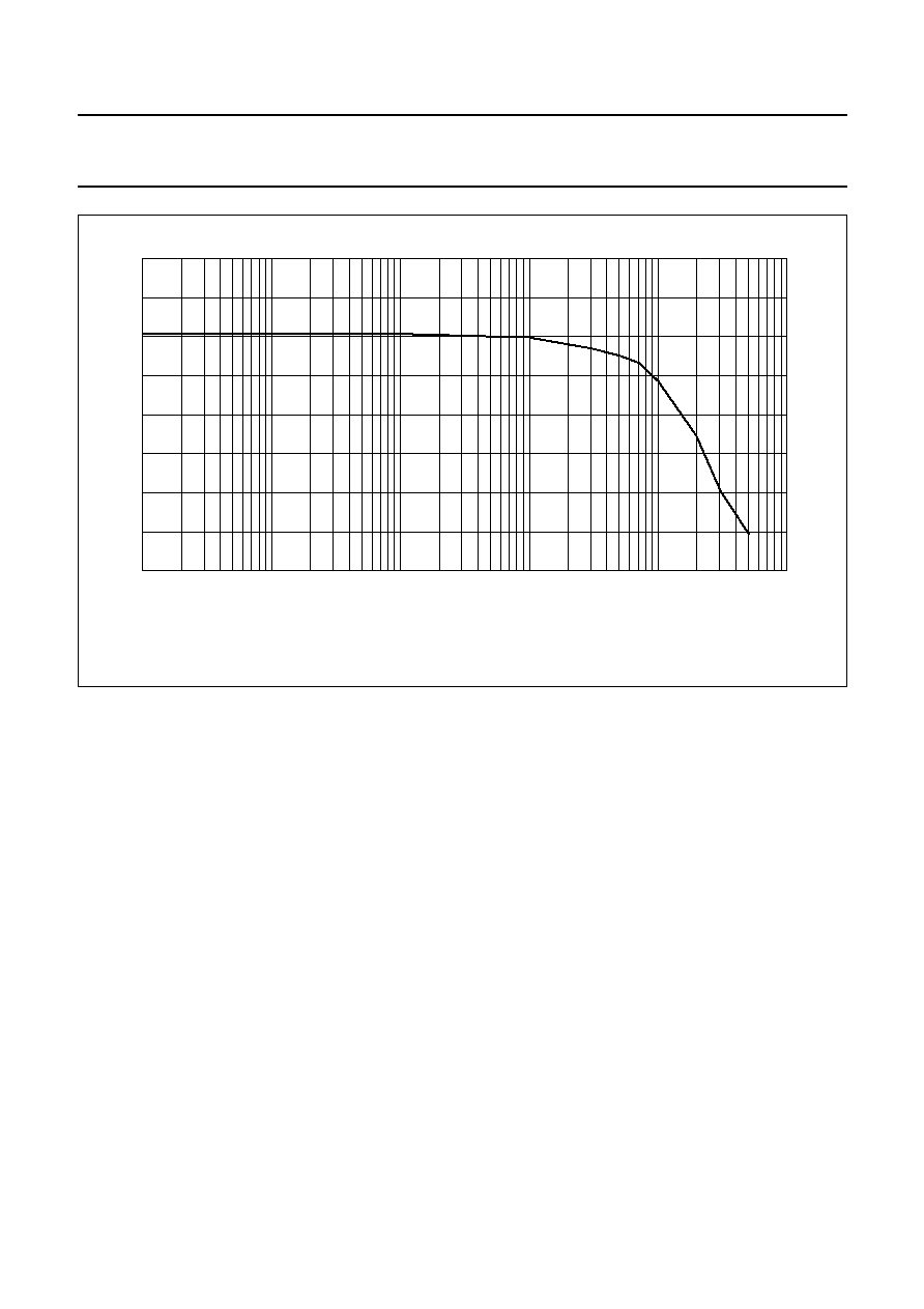
Fig.2 DC current gain; typical values.
V
CE
=
-
1 V.
handbook, full pagewidth
0
80
160
hFE
40
120
MGD841
-
10
-
1
-
1
IC (mA)
-
10
-
10
2
-
10
4
-
10
3
1999 Apr 23
5
Philips Semiconductors
Product specification
PNP medium power transistor
BDP32
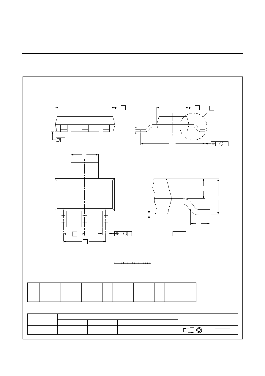
PACKAGE OUTLINE
UNIT
A
1
b
p
c
D
E
e
1
H
E
L
p
Q
y
w
v
REFERENCES
OUTLINE
VERSION
EUROPEAN
PROJECTION
ISSUE DATE
IEC
JEDEC
EIAJ
mm
0.10
0.01
1.8
1.5
0.80
0.60
b
1
3.1
2.9
0.32
0.22
6.7
6.3
3.7
3.3
2.3
e
4.6
7.3
6.7
1.1
0.7
0.95
0.85
0.1
0.1
0.2
DIMENSIONS (mm are the original dimensions)
SOT223
96-11-11
97-02-28
w
M
b
p
D
b
1
e
1
e
A
A
1
L
p
Q
detail X
H
E
E
v
M
A
A
B
B
c
y
0
2
4 mm
scale
A
X
1
3
2
4
Plastic surface mounted package; collector pad for good heat transfer; 4 leads
SOT223