 | –≠–ª–µ–∫—Ç—Ä–æ–Ω–Ω—ã–π –∫–æ–º–ø–æ–Ω–µ–Ω—Ç: BF1108 | –°–∫–∞—á–∞—Ç—å:  PDF PDF  ZIP ZIP |

DATA SHEET
Product specification
Supersedes data of 1999 Aug 19
1999 Nov 18
DISCRETE SEMICONDUCTORS
BF1108; BF1108R
Silicon RF switches

1999 Nov 18
2
Philips Semiconductors
Product specification
Silicon RF switches
BF1108; BF1108R
FEATURES
∑
Specially designed for low loss RF switching
up to 1 GHz.
APPLICATIONS
∑
Various RF switching applications such as:
≠ Passive loop through for VCR tuner
≠ Transceiver switching.
DESCRIPTION
These switches are a combination of a depletion type
field-effect transistor and a bandswitching diode in an
SOT143B (BF1108) or SOT143R (BF1108R) package.
The low loss and high isolation capabilities of these
devices provide excellent RF switching functions. The
gate of the MOSFET can be isolated from ground with the
diode, resulting in low losses. Integrated diodes between
gate and source and between gate and drain protect
against excessive input voltage surges.
PINNING
Note
1. Drain and source are interchangeable.
PIN
DESCRIPTION
1
FET gate; diode anode
2
diode cathode
3
source; note 1
4
drain; note 1
handbook, 2 columns
Top view
MSB014
1
2
3
4
Fig.1 Simplified outline (SOT143B).
Marking code: NGp.
handbook, 2 columns
Top view
MSB035
1
2
4
3
Fig.2 Simplified outline (SOT143R).
Marking code: NHp.
QUICK REFERENCE DATA
SYMBOL
PARAMETER
CONDITIONS
MIN.
TYP.
MAX.
UNIT
s
21(on)
2
losses (on-state)
R
S
= R
L
= 50
;
f
1 GHz
-
-
2
dB
s
21(off)
2
isolation (off-state)
30
-
-
dB
R
DSon
drain-source on-resistance
V
CS
= 0; I
D
= 1 mA
-
12
20
V
GSoff
pinch-off voltage
I
D
= 20
µ
A; V
DS
= 1 V
-
-
3
-
4
V
CAUTION
This product is supplied in anti-static packing to prevent damage caused by electrostatic discharge during transport
and handling. For further information, refer to Philips specs.: SNW-EQ-608, SNW-FQ-302A and SNW-FQ-302B.
1999 Nov 18
3
Philips Semiconductors
Product specification
Silicon RF switches
BF1108; BF1108R
LIMITING VALUES
In accordance with the Absolute Maximum Rating System (IEC 134).
THERMAL CHARACTERISTICS
Note
1. Soldering point of FET gate and diode anode lead.
STATIC CHARACTERISTICS
T
j
= 25
∞
C unless otherwise specified.
SYMBOL
PARAMETER
MIN.
MAX.
UNIT
FET
V
DS
drain-source voltage
-
3
V
V
SD
source-drain voltage
-
3
V
V
DG
drain-gate voltage
-
7
V
V
SG
source-gate voltage
-
7
V
I
D
drain current
-
10
mA
Diode
V
R
continuous reverse voltage
-
35
V
I
F
continuous forward current
-
100
mA
FET and diode
T
stg
storage temperature
-
65
+150
∞
C
T
j
junction temperature
-
150
∞
C
SYMBOL
PARAMETER
CONDITIONS
VALUE
UNIT
R
th j-s
thermal resistance from junction to soldering point note 1
250
K/W
SYMBOL
PARAMETER
CONDITIONS
MIN.
TYP.
MAX. UNIT
FET
V
(BR)GSS
gate-source breakdown voltage
V
DS
= 0; I
GS
= 0.1 mA
7
-
-
V
V
GSoff
gate-source pinch-off voltage
V
DS
= 1 V; I
D
= 20
µ
A
-
-
3
-
4
V
I
DSX
drain-source leakage current
V
GS
=
-
5 V; V
DS
= 2 V
-
-
10
µ
A
I
GSS
gate cut-off current
V
GS
=
-
5 V; V
DS
= 0
-
-
100
nA
R
DSon
drain-source on-state resistance
V
GS
= 0; I
D
= 1 mA
-
12
20
Diode
V
F
forward voltage
I
F
= 10 mA
-
-
1
V
I
R
reverse current
V
R
= 25 V
-
-
50
nA
V
R
= 20 V; T
amb
= 75
∞
C
-
-
1
µ
A

1999 Nov 18
4
Philips Semiconductors
Product specification
Silicon RF switches
BF1108; BF1108R
DYNAMIC CHARACTERISTICS
Common cathode; T
amb
= 25
∞
C.
Notes
1. I
F
= diode forward current.
2. C
ic
is the series connection of C
sg
and C
gc
; C
oc
is the series connection of C
dg
and C
gc
.
3. Guaranteed on AQL basis; inspection level S4, AQL 1.0.
SYMBOL
PARAMETER
CONDITIONS
MIN.
TYP.
MAX.
UNIT
FET and diode
s
21(on)
2
losses (on-state)
V
SC
= V
DC
= 0; R
S
= R
L
= 50
;
I
F
= 0; note 1; f
1 GHz
-
-
2
dB
V
SC
= V
DC
= 0; R
S
= R
L
= 50
; I
F
= 0;
f = 1 GHz
-
1.3
-
dB
V
SC
= V
DC
= 0; R
S
= R
L
= 75
; I
F
= 0;
f
1 GHz
-
-
3
dB
s
21(off)
2
isolation (off-state)
V
SC
= V
DC
= 5 V; R
S
= R
L
= 50
;
I
F
= 1 mA; f
1 GHz
30
-
-
dB
V
SC
= V
DC
= 5 V; R
S
= R
L
= 50
;
I
F
= 1 mA; f = 1 GHz
-
38
-
dB
V
SC
= V
DC
= 5 V; R
S
= R
L
= 75
;
I
F
= 1 mA; f
1 GHz
30
-
-
dB
R
DSon
drain-source on-resistance V
CS
= 0; I
D
= 1 mA
-
12
20
C
ic
input capacitance; note 2
V
SC
= V
DC
= 5 V; I
F
= 1 mA; f = 1 MHz
-
1
-
pF
V
SC
= V
DC
= 0; I
F
= 0; f = 1 MHz
-
0.65
0.9
pF
C
oc
output capacitance; note 2
V
SC
= V
DC
= 5 V; I
F
= 1 mA; f = 1 MHz
-
1
-
pF
V
SC
= V
DC
= 0; I
F
= 0; f = 1 MHz
-
0.65
0.9
pF
Diode
C
d
diode capacitance
f = 1 MHz; V
R
= 0
-
1.1
-
pF
r
D
diode forward resistance
I
F
= 2 mA; f = 100 MHz; note 3
-
-
0.7
handbook, halfpage
MBL027
d
s
s
SOT143B
SOT143R
d
g, a
c
c
g, a
Fig.3 Simplified diagram.
1999 Nov 18
5
Philips Semiconductors
Product specification
Silicon RF switches
BF1108; BF1108R
handbook, halfpage
0
400
1200
0
-
1
-
3
-
4
-
2
800
MGS357
f (MHz)
|s21(on)|
2
(dB)
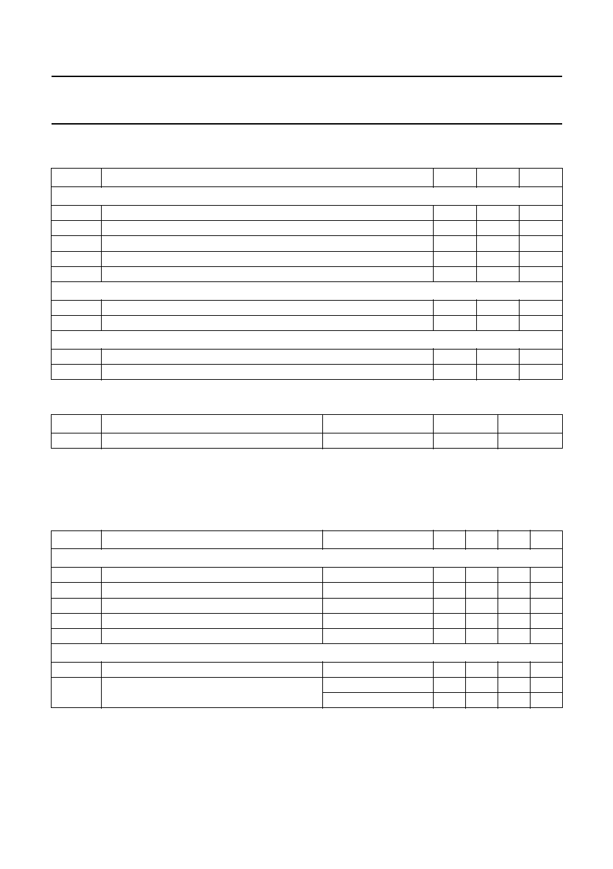
Fig.4
Losses (on-state) as a function of
frequency; typical values.
V
SC
= V
DC
= 0 V; R
S
= R
L
= 50
; I
F
= 0 mA (diode forward current);
Measured in test circuit (Fig.6).
handbook, halfpage
0
400
1200
0
-
40
-
60
-
20
800
MGS358
f (MHz)
|s21(off)|
2
(dB)
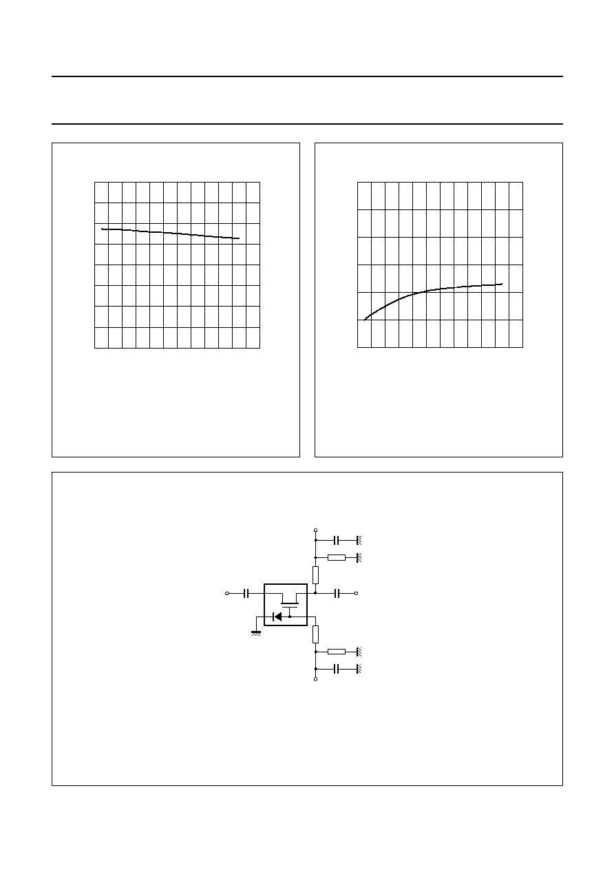
Fig.5
Isolation (off-state) as a function of
frequency; typical values.
V
SC
= V
DC
= 5 V; R
S
= R
L
= 50
; I
F
= 1 mA (diode forward current);
Measured in test circuit (Fig.6).
handbook, full pagewidth
MBL028
1 nF
1 nF
V
V
1 nF
1 nF
50
input
50
output
4.7 k
47 k
BF1108/BF1108R
100 k
100 k
Fig.6 Test circuit.
On-state: V = 0 V.
Off-state: V = 5 V.