
1.
Product profile
1.1 General description
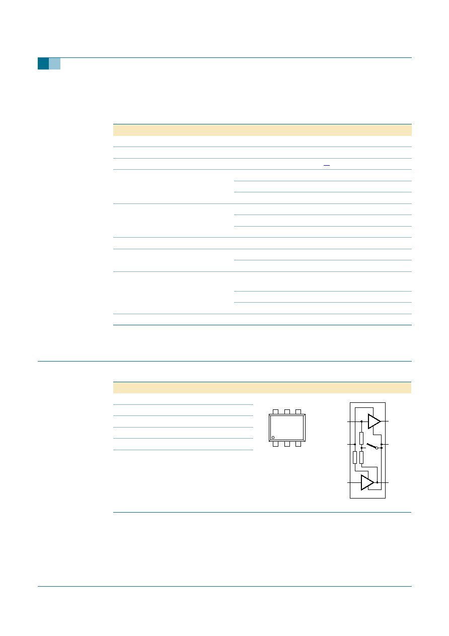
The BF1208 is a combination of two dual gate MOSFET amplifiers with shared source
and gate2 leads and an integrated switch. The integrated switch is operated by the gate1
bias of amplifier B.
The source and substrate are interconnected. Internal bias circuits enable
DC stabilization and a very good cross-modulation performance during Automatic Gain
Control (AGC). Integrated diodes between the gates and source protect against excessive
input voltage surges. The transistor has a SOT666 micro-miniature plastic package.
1.2 Features
s
Two low noise gain controlled amplifiers in a single package. One with a fully
integrated bias and one with a partly integrated bias
s
Internal switch to save external components
s
Superior cross-modulation performance during AGC
s
High forward transfer admittance
s
High forward transfer admittance to input capacitance ratio
1.3 Applications
s
Gain controlled low noise amplifiers for VHF and UHF applications with 5 V supply
voltage
x
digital and analog television tuners
x
professional communication equipment
BF1208
Dual N-channel dual gate MOSFET
Rev. 01 -- 16 March 2005
Product data sheet
CAUTION
This device is sensitive to ElectroStatic Discharge (ESD). Therefore care should be taken
during transport and handling.
MSC895
9397 750 14254
� Koninklijke Philips Electronics N.V. 2005. All rights reserved.
Product data sheet
Rev. 01 -- 16 March 2005
2 of 22
Philips Semiconductors
BF1208
Dual N-channel dual gate MOSFET
1.4 Quick reference data
[1]
T
sp
is the temperature at the soldering point of the source lead.
2.
Pinning information
Table 1:
Quick reference data
Per MOSFET unless otherwise specified.
Symbol Parameter
Conditions
Min
Typ
Max Unit
V
DS
drain-source voltage (DC)
-
-
6
V
I
D
drain current (DC)
-
-
30
mA
P
tot
total power dissipation
T
sp
109
�
C
[1]
-
-
180
mW
|
y
fs
|
forward transfer admittance
f = 1 MHz
amplifier A; I
D
= 19 mA
26
31
41
mS
amplifier B; I
D
= 13 mA
28
33
43
mS
C
iss(G1)
input capacitance at gate1
f = 1 MHz
amplifier A
-
2.2
2.7
pF
amplifier B
-
2.0
2.5
pF
C
rss
reverse transfer capacitance f = 1 MHz
-
20
-
fF
NF
noise figure
amplifier A; f = 400 MHz
-
1.3
1.9
dB
amplifier B; f = 800 MHz
-
1.4
2.1
dB
Xmod
cross-modulation
input level for k = 1 % at
40 dB AGC
amplifier A
100
105
-
dB
�
V
amplifier B
100
103
-
dB
�
V
T
j
junction temperature
-
-
150
�
C
Table 2:
Discrete pinning
Pin
Description
Simplified outline
Symbol
1
gate1 (AMP A)
2
gate2
3
gate1 (AMP B)
4
drain (AMP B)
5
source
6
drain (AMP A)
1
2
3
4
5
6
sym089
G1B
G1A
G2
S
DA
DB
AMP B
AMP A
9397 750 14254
� Koninklijke Philips Electronics N.V. 2005. All rights reserved.
Product data sheet
Rev. 01 -- 16 March 2005
3 of 22
Philips Semiconductors
BF1208
Dual N-channel dual gate MOSFET
3.
Ordering information
4.
Marking
5.
Limiting values
[1]
T
sp
is the temperature at the soldering point of the source lead.
Table 3:
Ordering information
Type number
Package
Name
Description
Version
BF1208
-
plastic surface mounted package; 6 leads
SOT666
Table 4:
Marking codes
Type number
Marking code
BF1208
2L
Table 5:
Limiting values
In accordance with the Absolute Maximum Rating System (IEC 60134).
Symbol
Parameter
Conditions
Min
Max
Unit
Per MOSFET
V
DS
drain-source voltage (DC)
-
6
V
I
D
drain current (DC)
-
30
mA
I
G1
gate1 current
-
�
10
mA
I
G2
gate2 current
-
�
10
mA
P
tot
total power dissipation
T
sp
109
�
C
[1]
-
180
mW
T
stg
storage temperature
-
65
+150
�
C
T
j
junction temperature
-
150
�
C
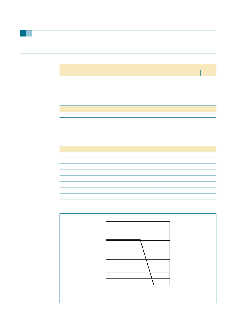
Fig 1.
Power derating curve
T
sp
(�C)
0
200
150
50
100
001aac193
100
150
50
200
250
P
tot
(mW)
0

9397 750 14254
� Koninklijke Philips Electronics N.V. 2005. All rights reserved.
Product data sheet
Rev. 01 -- 16 March 2005
4 of 22
Philips Semiconductors
BF1208
Dual N-channel dual gate MOSFET
6.
Thermal characteristics
7.
Static characteristics
[1]
R
G1
connects gate1 (B) to V
GG
= 0 V (see
Figure 3
).
[2]
R
G1
connects gate1 (B) to V
GG
= 5 V (see
Figure 3
).
Table 6:
Thermal characteristics
Symbol
Parameter
Conditions
Typ
Unit
R
th(j-sp)
thermal resistance from junction to solder point
225
K/W
Table 7:
Static characteristics
T
j
= 25
�
C; unless otherwise specified.
Symbol
Parameter
Conditions
Min
Typ
Max Unit
Per MOSFET; unless otherwise specified
V
(BR)DSS
drain-source breakdown voltage
V
G1-S
= V
G2-S
= 0 V; I
D
= 10
�
A
amplifier A
6
-
-
V
amplifier B
6
-
-
V
V
(BR)G1-SS
gate1-source breakdown voltage
V
G2-S
= V
DS
= 0 V; I
G1-S
= 10 mA
6
-
10
V
V
(BR)G2-SS
gate2-source breakdown voltage
V
G1-S
= V
DS
= 0 V; I
G2-S
= 10 mA
6
-
10
V
V
F(S-G1)
forward source-gate1 voltage
V
G2-S
= V
DS
= 0 V; I
S-G1
= 10 mA
0.5
-
1.5
V
V
F(S-G2)
forward source-gate2 voltage
V
G1-S
= V
DS
= 0 V; I
S-G2
= 10 mA
0.5
-
1.5
V
V
G1-S(th)
gate1-source threshold voltage
V
DS
= 5 V; V
G2-S
= 4 V; I
D
= 100
�
A
0.3
-
1.0
V
V
G2-S(th)
gate2-source threshold voltage
V
DS
= 5 V; V
G1-S
= 5 V; I
D
= 100
�
A
0.4
-
1.0
V
I
DSX
drain-source current
V
G2-S
= 4 V; V
DS(B)
= 5 V; R
G1
= 150 k
amplifier A; V
DS(A)
= 5 V
[1]
14
-
24
mA
amplifier B; V
DS(B)
= 5 V
[2]
9
-
17
mA
I
G1-S
gate1 cut-off current
V
G2-S
= V
DS(A)
= 0 V
amplifier A; V
G1-S(A)
= 5 V; I
D(B)
= 0 A
-
-
50
nA
amplifier B; V
G1-S(B)
= 5 V; V
DS(B)
= 0 V
-
-
50
nA
I
G2-S
gate2 cut-off current
V
G2-S
= 4 V; V
G1-S(B)
= 0 V;
V
G1-S(A)
= V
DS(A)
= V
DS(B)
= 0 V
-
-
20
nA
9397 750 14254
� Koninklijke Philips Electronics N.V. 2005. All rights reserved.
Product data sheet
Rev. 01 -- 16 March 2005
5 of 22
Philips Semiconductors
BF1208
Dual N-channel dual gate MOSFET
8.
Dynamic characteristics
8.1 Dynamic characteristics for amplifier A
(1) I
D(B)
; R
G1
= 120 k
.
(2) I
D(B)
; R
G1
= 150 k
.
(3) I
D(B)
; R
G1
= 180 k
.
(4) I
D(A)
; R
G1
= 180 k
.
(5) I
D(A)
; R
G1
= 150 k
.
(6) I
D(A)
; R
G1
= 120 k
.
V
GG
= 5 V: amplifier A is off; amplifier B is on.
V
GG
= 0 V: amplifier A is on; amplifier B is off.
Fig 2.
Drain currents of MOSFET A and B as a
function of gate1 supply voltage
Fig 3.
Functional diagram
001aaa552
8
12
4
16
20
I
D
(mA)
0
V
GG
(V)
0
5
4
2
3
1
(2)
(5)
(4)
(6)
(3)
(1)
001aac205
R
G1
V
GG
G1B
G2
G1A
DB
S
DA
Table 8:
Dynamic characteristics for amplifier A
[1]
Common source; T
amb
= 25
�
C; V
G2-S
= 4 V; V
DS
= 5 V; I
D
= 19 mA; unless otherwise specified.
Symbol
Parameter
Conditions
Min
Typ
Max
Unit
|
y
fs
|
forward transfer admittance
T
j
= 25
�
C
26
31
41
mS
C
iss(G1)
input capacitance at gate1
f = 1 MHz
-
2.2
2.7
pF
C
iss(G2)
input capacitance at gate2
f = 1 MHz
-
3.0
-
pF
C
oss
output capacitance
f = 1 MHz
-
0.9
-
pF
C
rss
reverse transfer capacitance
f = 1 MHz
-
20
-
fF
G
tr
power gain
B
S
= B
S(opt)
; B
L
= B
L(opt)
f = 200 MHz; G
S
= 2 mS; G
L
= 0.5 mS
32
36
40
dB
f = 400 MHz; G
S
= 2 mS; G
L
= 1 mS
28
32
36
dB
f = 800 MHz; G
S
= 3.3 mS; G
L
= 1 mS
23
27
32
dB
NF
noise figure
f = 11 MHz; G
S
= 20 mS; B
S
= 0 S
-
3.0
-
dB
f = 400 MHz; Y
S
= Y
S(opt)
-
1.3
1.9
dB
f = 800 MHz; Y
S
= Y
S(opt)
-
1.4
2.1
dB