 | –≠–ª–µ–∫—Ç—Ä–æ–Ω–Ω—ã–π –∫–æ–º–ø–æ–Ω–µ–Ω—Ç: BF1212R | –°–∫–∞—á–∞—Ç—å:  PDF PDF  ZIP ZIP |
Document Outline
- FEATURES
- APPLICATIONS
- DESCRIPTION
- PINNING
- QUICK REFERENCE DATA
- ORDERING INFORMATION
- LIMITING VALUES
- THERMAL CHARACTERISTICS
- STATIC CHARACTERISTICS
- DYNAMIC CHARACTERISTICS
- PACKAGE OUTLINES
- DATA SHEET STATUS
- DEFINITIONS
- DISCLAIMERS

DATA SHEET
Product specification
2003 Nov 14
DISCRETE SEMICONDUCTORS
BF1212; BF1212R; BF1212WR
N-channel dual-gate MOS-FETs
2003 Nov 14
2
Philips Semiconductors
Product specification
N-channel dual-gate MOS-FETs
BF1212; BF1212R; BF1212WR
FEATURES
∑
Short channel transistor with high forward transfer
admittance to input capacitance ratio
∑
Low noise gain controlled amplifier
∑
Excellent low frequency noise performance
∑
Partly internal self-biasing circuit to ensure good
cross-modulation performance during AGC and good
DC stabilization.
APPLICATIONS
∑
Gain controlled low noise VHF and UHF amplifiers for
5 V digital and analog television tuner applications.
DESCRIPTION
Enhancement type N-channel field-effect transistor with
source and substrate interconnected. Integrated diodes
between gates and source protect against excessive input
voltage surges. The BF1212, BF1212R and BF1212WR
are encapsulated in the SOT143B, SOT143R and
SOT343R plastic packages respectively.
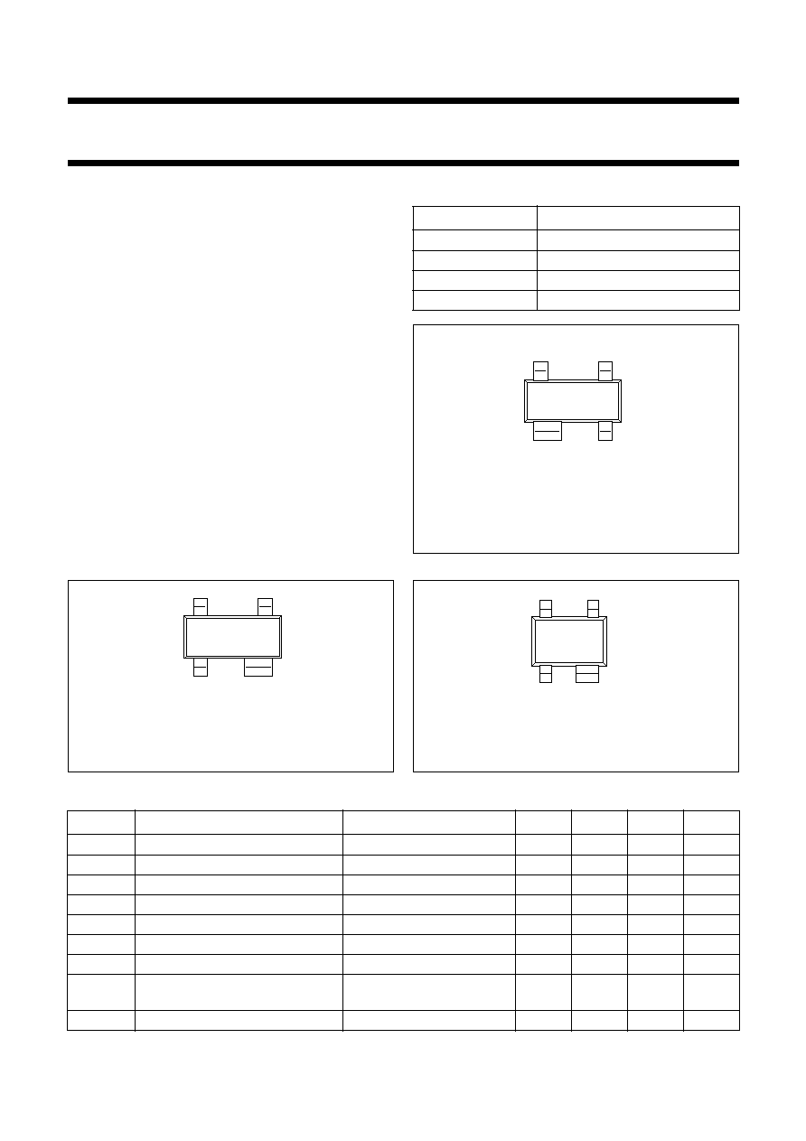
PINNING
PIN
DESCRIPTION
1
source
2
drain
3
gate 2
4
gate 1
handbook, 2 columns
Top view
MSB014
1
2
3
4
Fig.1 Simplified outline (SOT143B).
BF1212; marking code: LGp
handbook, 2 columns
Top view
MSB035
1
2
4
3
Fig.2 Simplified outline (SOT143R).
BF1212R; marking code: LKp
handbook, halfpage
Top view
MSB842
2
1
4
3
Fig.3 Simplified outline (SOT343R).
BF1212WR; marking code: ML
QUICK REFERENCE DATA
SYMBOL
PARAMETER
CONDITIONS
MIN.
TYP.
MAX.
UNIT
V
DS
drain-source voltage
-
-
6
V
I
D
drain current
-
-
30
mA
P
tot
total power dissipation
-
-
180
mW
y
fs
forward transfer admittance
28
33
43
mS
C
ig1-ss
input capacitance at gate 1
-
1.7
2.2
pF
C
rss
reverse transfer capacitance
f = 1 MHz
-
15
30
fF
F
noise figure
f = 800 MHz
-
1.1
1.8
dB
X
mod
cross-modulation
input level for k = 1 % at
40 dB AGC
100
104
-
dB
µ
V
T
j
junction temperature
-
-
150
∞
C

2003 Nov 14
3
Philips Semiconductors
Product specification
N-channel dual-gate MOS-FETs
BF1212; BF1212R; BF1212WR
ORDERING INFORMATION
LIMITING VALUES
In accordance with the Absolute Maximum Rating System (IEC 60134).
Note
1. T
s
is the temperature of the soldering point of the source lead.
THERMAL CHARACTERISTICS
CAUTION
This product is supplied in anti-static packing to prevent damage caused by electrostatic discharge during transport
and handling. For further information, refer to Philips specs.: SNW-EQ-608, SNW-FQ-302A and SNW-FQ-302B.
TYPE NUMBER
PACKAGE
NAME
DESCRIPTION
VERSION
BF1212
-
plastic surface mounted package; 4 leads
SOT143B
BF1212R
-
plastic surface mounted package; reverse pinning; 4 leads
SOT143R
BF1212WR
-
plastic surface mounted package; reverse pinning; 4 leads
SOT343R
SYMBOL
PARAMETER
CONDITIONS
MIN.
MAX.
UNIT
V
DS
drain-source voltage
-
6
V
I
D
drain current (DC)
-
30
mA
I
G1
gate 1 current
-
±
10
mA
I
G2
gate 2 current
-
±
10
mA
P
tot
total power dissipation
BF1212; BF1212R
T
s
116
∞
C; note 1
-
180
mW
BF1212WR
T
s
122
∞
C; note 1
-
180
mW
T
stg
storage temperature
-
65
+150
∞
C
T
j
junction temperature
-
150
∞
C
SYMBOL
PARAMETER
VALUE
UNIT
R
th j-s
thermal resistance from junction to soldering point
BF1212; BF1212R
185
K/W
BF1212WR
155
K/W

2003 Nov 14
4
Philips Semiconductors
Product specification
N-channel dual-gate MOS-FETs
BF1212; BF1212R; BF1212WR
handbook, halfpage
0
50
100
200
250
0
200
150
150
100
50
MDB828
(2)
(1)
Ptot
(mW)
Ts (
∞
C)
Fig.4 Power derating curve.
(1) BF1212WR.
(2) BF1212; BF1212R.
STATIC CHARACTERISTICS
T
j
= 25
∞
C unless otherwise specified.
Note
1. R
G1
connects G
1
to V
GG
= 5 V.
SYMBOL
PARAMETER
CONDITIONS
MIN.
MAX.
UNIT
V
(BR)DSS
drain-source breakdown voltage
V
G1-S
= V
G2-S
= 0 V; I
D
= 10
µ
A
6
-
V
V
(BR)G1-SS
gate 1-source breakdown voltage
V
G2-S
= V
DS
= 0 V; I
G1-S
= 10 mA
6
10
V
V
(BR)G2-SS
gate 2-source breakdown voltage
V
G1-S
= V
DS
= 0 V; I
G2-S
= 10 mA
6
10
V
V
(F)S-G1
forward source-gate 1 voltage
V
G2-S
= V
DS
= 0 V; I
S-G1
= 10 mA
0.5
1.5
V
V
(F)S-G2
forward source-gate 2 voltage
V
G1-S
= V
DS
= 0 V; I
S-G2
= 10 mA
0.5
1.5
V
V
G1-S(th)
gate 1-source threshold voltage
V
G2-S
= 4 V; V
DS
= 5 V; I
D
= 100
µ
A
0.3
1.0
V
V
G2-S(th)
gate 2-source threshold voltage
V
G1-S
= 5 V; V
DS
= 5 V; I
D
= 100
µ
A
0.35
1.0
V
I
DSX
drain-source current
V
G2-S
= 4 V; V
DS
= 5 V; R
G1
= 150 k
;
note 1
8
16
mA
I
G1-S
gate 1 cut-off current
V
G2-S
= V
DS
= 0 V; V
G1-S
= 5 V
-
50
nA
I
G2-S
gate 2 cut-off current
V
G1-S
= V
DS
= 0 V; V
G2-S
= 4 V
-
20
nA

2003 Nov 14
5
Philips Semiconductors
Product specification
N-channel dual-gate MOS-FETs
BF1212; BF1212R; BF1212WR
DYNAMIC CHARACTERISTICS
Common source; T
amb
= 25
∞
C; V
G2-S
= 4 V; V
DS
= 5 V; I
D
= 12 mA; unless otherwise specified.
Note
1. Measured in test circuit Fig.21.
SYMBOL
PARAMETER
CONDITIONS
MIN.
TYP.
MAX.
UNIT
y
fs
forward transfer admittance
pulsed; T
j
= 25
∞
C
28
33
43
mS
C
ig1-ss
input capacitance at gate 1
f = 1 MHz
-
1.7
2.2
pF
C
ig2-ss
input capacitance at gate 2
f = 1 MHz
-
1.1
-
pF
C
oss
output capacitance
f = 1 MHz
-
0.9
-
pF
C
rss
reverse transfer capacitance f = 1 MHz
-
15
30
fF
F
noise figure
f = 11 MHz; G
S
= 20 mS; B
S
= 0
-
4
-
dB
f = 400 MHz; Y
S
= Y
S (opt)
-
0.9
1.6
dB
f = 800 MHz; Y
S
= Y
S (opt)
-
1.1
1.8
dB
G
tr
power gain
f = 200 MHz; G
S
= 2 mS; B
S
= B
S (opt)
;
G
L
= 0.5 mS; B
L
= B
L (opt)
-
35
-
dB
f = 400 MHz; G
S
= 2 mS; B
S
= B
S (opt)
;
G
L
= 1 mS; B
L
= B
L (opt)
-
30
-
dB
f = 800 MHz; G
S
= 3.3 mS; B
S
= B
S (opt)
;
G
L
= 1 mS; B
L
= B
L (opt)
-
25
-
dB
X
mod
cross-modulation
input level for k = 1%; f
w
= 50 MHz;
f
unw
= 60 MHz; note 1
at 0 dB AGC
90
-
-
dB
µ
V
at 10 dB AGC
-
89
-
dB
µ
V
at 40 dB AGC
100
104
-
dB
µ
V