 | –≠–ª–µ–∫—Ç—Ä–æ–Ω–Ω—ã–π –∫–æ–º–ø–æ–Ω–µ–Ω—Ç: BF245B | –°–∫–∞—á–∞—Ç—å:  PDF PDF  ZIP ZIP |

DATA SHEET
Product specification
Supersedes data of April 1995
File under Discrete Semiconductors, SC07
1996 Jul 30
DISCRETE SEMICONDUCTORS
BF245A; BF245B; BF245C
N-channel silicon field-effect
transistors

1996 Jul 30
2
Philips Semiconductors
Product specification
N-channel silicon field-effect transistors
BF245A; BF245B; BF245C
FEATURES
∑
Interchangeability of drain and source connections
∑
Frequencies up to 700 MHz.
APPLICATIONS
∑
LF, HF and DC amplifiers.
DESCRIPTION
General purpose N-channel symmetrical junction
field-effect transistors in a plastic TO-92 variant package.
CAUTION
The device is supplied in an antistatic package. The
gate-source input must be protected against static
discharge during transport or handling.
PINNING
PIN
SYMBOL
DESCRIPTION
1
d
drain
2
s
source
3
g
gate
Fig.1
Simplified outline (TO-92 variant)
and symbol.
handbook, halfpage
1
3
2
MAM257
s
d
g
QUICK REFERENCE DATA
SYMBOL
PARAMETER
CONDITIONS
MIN.
TYP.
MAX.
UNIT
V
DS
drain-source voltage
-
-
±
30
V
V
GSoff
gate-source cut-off voltage
I
D
= 10 nA; V
DS
= 15 V
-
0.25
-
-
8
V
V
GSO
gate-source voltage
open drain
-
-
-
30
V
I
DSS
drain current
V
DS
= 15 V; V
GS
= 0
BF245A
2
-
6.5
mA
BF245B
6
-
15
mA
BF245C
12
-
25
mA
P
tot
total power dissipation
T
amb
= 75
∞
C
-
-
300
mW
y
fs
forward transfer admittance
V
DS
= 15 V; V
GS
= 0;
f = 1 kHz; T
amb
= 25
∞
C
3
-
6.5
mS
C
rs
reverse transfer capacitance
V
DS
= 20 V; V
GS
=
-
1 V;
f = 1 MHz; T
amb
= 25
∞
C
-
1.1
-
pF

1996 Jul 30
3
Philips Semiconductors
Product specification
N-channel silicon field-effect transistors
BF245A; BF245B; BF245C
LIMITING VALUES
In accordance with the Absolute Maximum Rating System (IEC 134).
Note
1. Device mounted on a printed-circuit board, minimum lead length 3 mm, mounting pad for drain lead minimum
10 mm
◊
10 mm.
THERMAL CHARACTERISTICS
STATIC CHARACTERISTICS
T
j
= 25
∞
C; unless otherwise specified.
Note
1. Measured under pulse conditions: t
p
= 300
µ
s;
0.02.
SYMBOL
PARAMETER
CONDITIONS
MIN.
MAX.
UNIT
V
DS
drain-source voltage
-
±
30
V
V
GDO
gate-drain voltage
open source
-
-
30
V
V
GSO
gate-source voltage
open drain
-
-
30
V
I
D
drain current
-
25
mA
I
G
gate current
-
10
mA
P
tot
total power dissipation
up to T
amb
= 75
∞
C;
-
300
mW
up to T
amb
= 90
∞
C; note 1
-
300
mW
T
stg
storage temperature
-
65
+150
∞
C
T
j
operating junction temperature
-
150
∞
C
SYMBOL
PARAMETER
CONDITIONS
VALUE
UNIT
R
th j-a
thermal resistance from junction to ambient
in free air
250
K/W
thermal resistance from junction to ambient
200
K/W
SYMBOL
PARAMETER
CONDITIONS
MIN.
MAX.
UNIT
V
(BR)GSS
gate-source breakdown voltage
I
G
=
-
1
µ
A; V
DS
= 0
-
30
-
V
V
GSoff
gate-source cut-off voltage
I
D
= 10 nA; V
DS
= 15 V
-
0.25
-
8.0
V
V
GS
gate-source voltage
I
D
= 200
µ
A; V
DS
= 15 V
BF245A
-
0.4
-
2.2
V
BF245B
-
1.6
-
3.8
V
BF245C
-
3.2
-
7.5
V
I
DSS
drain current
V
DS
= 15 V; V
GS
= 0; note 1
BF245A
2
6.5
mA
BF245B
6
15
mA
BF245C
12
25
mA
I
GSS
gate cut-off current
V
GS
=
-
20 V; V
DS
= 0
-
-
5
nA
V
GS
=
-
20 V; V
DS
= 0; T
j
= 125
∞
C
-
-
0.5
µ
A
1996 Jul 30
4
Philips Semiconductors
Product specification
N-channel silicon field-effect transistors
BF245A; BF245B; BF245C
DYNAMIC CHARACTERISTICS
Common source; T
amb
= 25
∞
C; unless otherwise specified.
SYMBOL
PARAMETER
CONDITIONS
MIN.
TYP.
MAX.
UNIT
C
is
input capacitance
V
DS
= 20 V; V
GS
=
-
1 V; f = 1 MHz
-
4
-
pF
C
rs
reverse transfer capacitance
V
DS
= 20 V; V
GS
=
-
1 V; f = 1 MHz
-
1.1
-
pF
C
os
output capacitance
V
DS
= 20 V; V
GS
=
-
1 V; f = 1 MHz
-
1.6
-
pF
g
is
input conductance
V
DS
= 15 V; V
GS
= 0; f = 200 MHz
-
250
-
µ
S
g
os
output conductance
V
DS
= 15 V; V
GS
= 0; f = 200 MHz
-
40
-
µ
S
y
fs
forward transfer admittance
V
DS
= 15 V; V
GS
= 0; f = 1 kHz
3
-
6.5
mS
V
DS
= 15 V; V
GS
= 0; f = 200 MHz
-
6
-
mS
y
rs
reverse transfer admittance
V
DS
= 15 V; V
GS
= 0; f = 200 MHz
-
1.4
-
mS
y
os
output admittance
V
DS
= 15 V; V
GS
= 0; f = 1 kHz
-
25
-
µ
S
f
gfs
cut-off frequency
V
DS
= 15 V; V
GS
= 0; g
fs
= 0.7 of its
value at 1 kHz
-
700
-
MHz
F
noise figure
V
DS
= 15 V; V
GS
= 0; f = 100 MHz;
R
G
= 1 k
(common source);
input tuned to minimum noise
-
1.5
-
dB
handbook, halfpage
-
10
-
10
-
3
-
10
-
2
-
10
-
1
-
1
150
50
0
MGE785
100
typ
Tj (
∞
C)
IGSS
(nA)
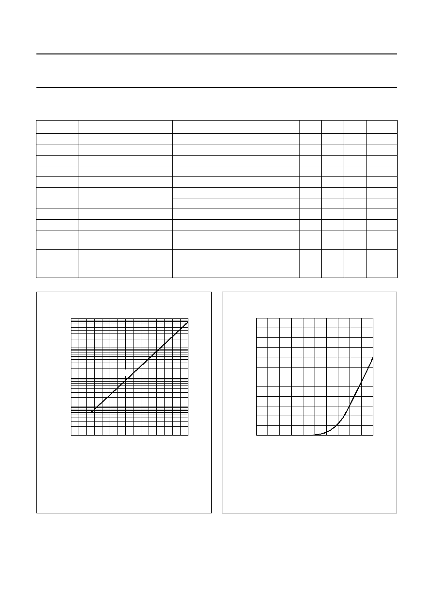
Fig.2
Gate leakage current as a function of
junction temperature; typical values.
V
DS
= 0; V
GS
=
-
20 V.
Fig.3
Transfer characteristics for BF245A;
typical values.
handbook, halfpage
VGS (V)
ID
(mA)
6
0
-
4
0
-
2
MGE789
5
4
3
2
1
V
DS
= 15 V; T
j
= 25
∞
C.
1996 Jul 30
5
Philips Semiconductors
Product specification
N-channel silicon field-effect transistors
BF245A; BF245B; BF245C
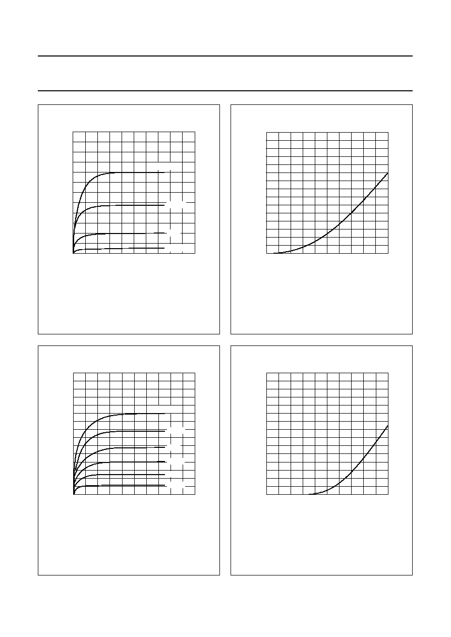
handbook, halfpage
VDS (V)
ID
(mA)
6
0
0
20
10
MBH555
5
4
3
2
1
VGS = 0 V
-
0.5 V
-
1 V
-
1.5 V
Fig.4
Output characteristics for BF245A;
typical values.
V
DS
= 15 V; T
j
= 25
∞
C.
Fig.5
Transfer characteristics for BF245B;
typical values.
V
DS
= 15 V; T
j
= 25
∞
C.
handbook, halfpage
VGS (V)
ID
(mA)
15
0
-
4
0
-
2
MGE787
10
5
handbook, halfpage
VDS (V)
ID
(mA)
15
0
0
20
10
MBH553
10
5
VGS = 0 V
-
0.5 V
-
1 V
-
1.5 V
-
2 V
-
2.5 V
Fig.6
Output characteristics for BF245B;
typical values.
V
DS
= 15 V; T
j
= 25
∞
C.
Fig.7
Transfer characteristics for BF245C;
typical values.
handbook, halfpage
VGS (V)
ID
(mA)
30
0
-
10
0
-
5
MGE788
20
10
V
DS
= 15 V; T
j
= 25
∞
C.