 | –≠–ª–µ–∫—Ç—Ä–æ–Ω–Ω—ã–π –∫–æ–º–ø–æ–Ω–µ–Ω—Ç: BF247C | –°–∫–∞—á–∞—Ç—å:  PDF PDF  ZIP ZIP |

DATA SHEET
Product specification
Supersedes data of April 1995
File under Discrete Semiconductors, SC07
1996 Jul 29
DISCRETE SEMICONDUCTORS
BF246A; BF246B; BF246C;
BF247A; BF247B; BF247C
N-channel silicon junction
field-effect transistors
1996 Jul 29
2
Philips Semiconductors
Product specification
N-channel silicon junction
field-effect transistors
BF246A; BF246B; BF246C;
BF247A; BF247B; BF247C
FEATURES
∑
Interchangeability of drain and source connections
∑
High I
DSS
range
∑
Frequency up to 450 MHz.
APPLICATIONS
∑
VHF and UHF amplifiers
∑
Mixers
∑
General purpose switching.
DESCRIPTION
General purpose N-channel symmetrical silicon junction
field-effect transistors in a plastic TO-92 variant package.
CAUTION
The device is supplied in an antistatic package. The
gate-source input must be protected against static
discharge during transport or handling.
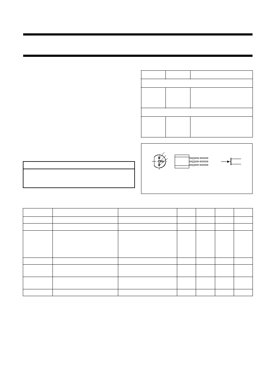
PINNING
PIN
SYMBOL
DESCRIPTION
BF246A; BF246B; BF246C
1
d
drain
2
g
gate
3
s
source
BF247A; BF247B; BF247C
1
d
drain
2
s
source
3
g
gate
Fig.1
Simplified outline (TO-92 variant)
and symbol.
handbook, halfpage
1
3
2
MAM257
s
d
g
QUICK REFERENCE DATA
SYMBOL
PARAMETER
CONDITIONS
MIN.
TYP.
MAX.
UNIT
V
DS
drain-source voltage
-
-
±
25
V
V
GSoff
gate-source cut-off voltage
I
D
= 10 nA; V
DS
= 15 V
-
0.6
-
-
14.5
V
I
DSS
drain current
V
DS
= 15 V; V
GS
= 0
BF246A; BF247A
30
-
80
mA
BF246B; BF247B
60
-
140
mA
BF246C; BF247C
110
-
250
mA
P
tot
total power dissipation
up to T
amb
= 50
∞
C
-
-
400
mW
y
fs
forward transfer admittance
I
D
= 10 mA; V
DS
= 15 V;
f = 1 kHz
8
-
-
mS
C
rs
reverse transfer capacitance
I
D
= 10 mA; V
DS
= 15 V;
f = 1 MHz
-
3.5
-
pF
T
j
operating junction temperature
-
-
150
∞
C
1996 Jul 29
3
Philips Semiconductors
Product specification
N-channel silicon junction
field-effect transistors
BF246A; BF246B; BF246C;
BF247A; BF247B; BF247C
LIMITING VALUES
In accordance with the Absolute Maximum Rating System (IEC 134).
THERMAL CHARACTERISTICS
STATIC CHARACTERISTICS
T
amb
= 25
∞
C; unless otherwise specified.
Note
1. Measured under pulse conditions: t
p
= 300
µ
s;
0.02.
DYNAMIC CHARACTERISTICS
T
amb
= 25
∞
C; unless otherwise specified.
SYMBOL
PARAMETER
CONDITIONS
MIN.
MAX.
UNIT
V
DS
drain-source voltage
-
±
25
V
I
G
gate current
-
10
mA
P
tot
total power dissipation
up to T
amb
= 50
∞
C
-
400
mW
T
stg
storage temperature
-
65
+150
∞
C
T
j
operating junction temperature
-
150
∞
C
SYMBOL
PARAMETER
CONDITIONS
VALUE
UNIT
R
th j-a
thermal resistance from junction to ambient
in free air
250
K/W
SYMBOL
PARAMETER
CONDITIONS
MIN.
TYP.
MAX.
UNIT
V
(BR)GSS
gate-source breakdown voltage
I
G
=
-
1
µ
A; V
DS
= 0
-
25
-
-
V
V
GSoff
gate-source cut-off voltage
I
D
= 10 nA; V
DS
= 15 V
-
0.6
-
-
14.5
V
V
GS
gate-source voltage
I
D
= 200
µ
A; V
DS
= 15 V
BF246A; BF247A
-
1.5
-
-
4.0
V
BF246B; BF247B
-
3.0
-
-
7.0
V
BF246C; BF247C
-
5.5
-
-
12.0
V
I
DSS
drain current
V
GS
= 0; V
DS
= 15 V; note 1
BF246A; BF247A
30
-
80
mA
BF246B; BF247B
60
-
140
mA
BF246C; BF247C
110
-
250
mA
I
GSS
gate leakage current
V
GS
=
-
15 V; V
DS
= 0
-
-
-
5
nA
SYMBOL
PARAMETER
CONDITIONS
MIN.
TYP.
MAX.
UNIT
C
is
input capacitance
I
D
= 10 mA; f = 1 MHz; V
DS
= 15 V
-
11
-
pF
C
rs
reverse transfer capacitance
I
D
= 10 mA; f = 1 MHz; V
DS
= 15 V
-
3.5
-
pF
C
os
output capacitance
I
D
= 10 mA; f = 1 MHz; V
DS
= 15 V
-
5
-
pF
y
fs
forward transfer admittance
I
D
= 10 mA; f = 1 kHz; V
DS
= 15 V
8
17
-
mS
f
gfs
cut-off frequency
g
fs
= 0.7 of its value at 1 kHz; V
GS
= 0
-
450
-
MHz
1996 Jul 29
4
Philips Semiconductors
Product specification
N-channel silicon junction
field-effect transistors
BF246A; BF246B; BF246C;
BF247A; BF247B; BF247C
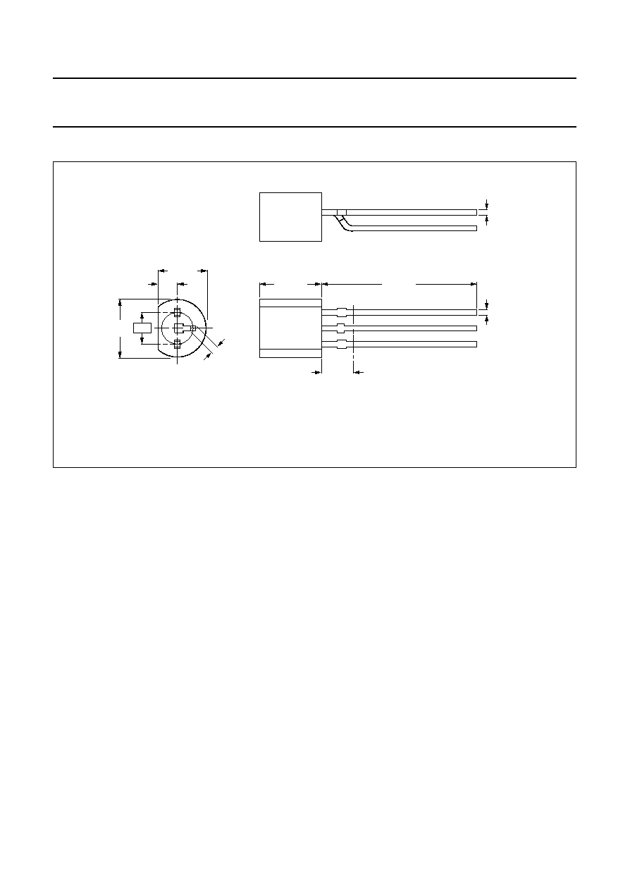
PACKAGE OUTLINE
Fig.2 TO-92 variant.
Dimensions in mm.
(1) Terminal dimensions in this zone are uncontrolled.
handbook, full pagewidth
MBC015 - 1
2.54
4.8
max
4.2 max
0.66
0.56
1
2
3
5.2 max
12.7 min
2.5 max
(1)
0.48
0.40
0.40
min
1.7
1.4
1996 Jul 29
5
Philips Semiconductors
Product specification
N-channel silicon junction
field-effect transistors
BF246A; BF246B; BF246C;
BF247A; BF247B; BF247C
DEFINITIONS
LIFE SUPPORT APPLICATIONS
These products are not designed for use in life support appliances, devices, or systems where malfunction of these
products can reasonably be expected to result in personal injury. Philips customers using or selling these products for
use in such applications do so at their own risk and agree to fully indemnify Philips for any damages resulting from such
improper use or sale.
Data Sheet Status
Objective specification
This data sheet contains target or goal specifications for product development.
Preliminary specification
This data sheet contains preliminary data; supplementary data may be published later.
Product specification
This data sheet contains final product specifications.
Limiting values
Limiting values given are in accordance with the Absolute Maximum Rating System (IEC 134). Stress above one or
more of the limiting values may cause permanent damage to the device. These are stress ratings only and operation
of the device at these or at any other conditions above those given in the Characteristics sections of the specification
is not implied. Exposure to limiting values for extended periods may affect device reliability.
Application information
Where application information is given, it is advisory and does not form part of the specification.