
DATA SHEET
Product specification
File under Discrete Semiconductors, SC07
December 1990
DISCRETE SEMICONDUCTORS
BF410A to D
N-channel silicon field-effect
transistors
December 1990
2
Philips Semiconductors
Product specification
N-channel silicon field-effect transistors
BF410A to D
DESCRIPTION
Asymmetrical N-channel planar
epitaxial junction field-effect
transistors in a plastic TO-92 variant;
intended for applications up to the
VHF range.
These FETs can be supplied in four
I
DSS
groups. Special features are the
low feedback capacitance and the low
noise figure. Thanks to these special
features the BF410 is very suitable for
applications such as the RF stages in
FM portables (type A), car radios
(type B) and mains radios (type C) or
the mixer stage (type D).
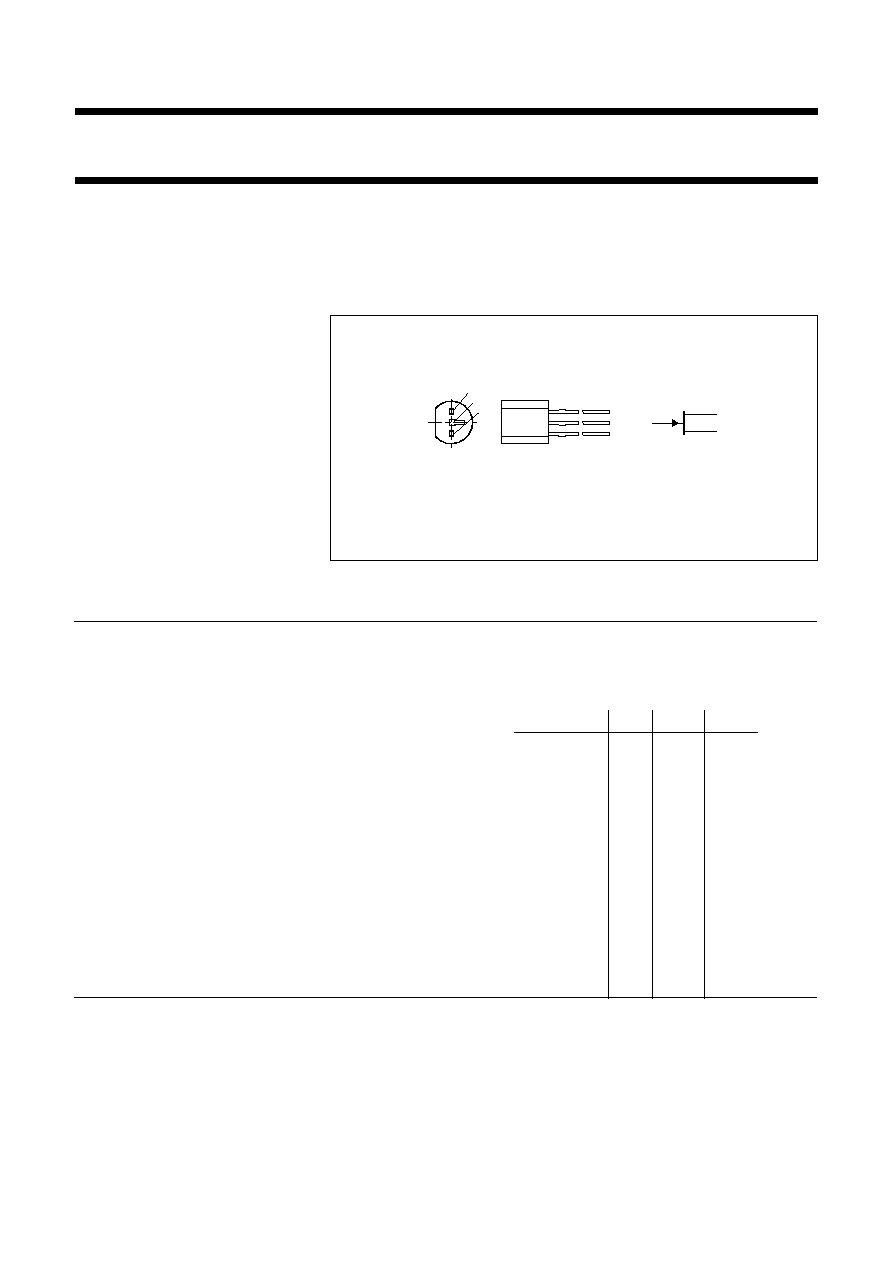
PINNING - TO-92 VARIANT
1
= drain
2
= source
3
= gate
Fig.1 Simplified outline and symbol
handbook, halfpage
1
3
2
MAM257
s
d
g
QUICK REFERENCE DATA
Drain-source voltage
V
DS
max.
20
V
Drain current (DC or average)
I
D
max.
30
mA
Total power dissipation
up to T
amb
= 75
�
C
P
tot
max.
300
mW
BF410A
B
C
D
Drain current
V
DS
= 10 V; V
GS
= 0
I
DSS
min.
0.7
2.5
6
10 mA
max.
3.0
7.0
12
18 mA
Transfer admittance
V
DS
= 10 V; V
GS
= 0; f = 1 kHz
y
fs
min.
2.5
4
6
7 mS
Feedback capacitance
V
DS
= 10 V; V
GS
= 0
C
rs
typ.
0.5
0.5
-
-
pF
V
DS
= 10 V; I
D
= 5 mA
C
rs
typ.
-
-
0.5
0.5 pF
Noise figure at optimum source admittance
G
S
= 1 mS;
-
B
S
= 3 mS; f = 100 MHz
V
DS
= 10 V; V
GS
= 0
F
typ.
1.5
1.5
-
-
dB
V
DS
= 10 V; I
D
= 5 mA
F
typ.
-
-
1.5
1.5 dB

December 1990
3
Philips Semiconductors
Product specification
N-channel silicon field-effect transistors
BF410A to D
RATINGS
Limiting values in accordance with the Absolute Maximum System (IEC 134)
THERMAL RESISTANCE
STATIC CHARACTERISTICS
T
amb
= 25
�
C
Drain-source voltage
V
DS
max.
20 V
Drain-gate voltage (open source)
V
DGO
max.
20 V
Drain current (DC or average)
I
D
max.
30 mA
Gate current
�
I
G
max.
10 mA
Total power dissipation up to T
amb
= 75
�
C
P
tot
max.
300 mW
Storage temperature range
T
stg
-
65 to
+
150
�
C
Junction temperature
T
j
max.
150
�
C
From junction to ambient in free air
R
th j-a
=
250 K/W
Gate cut-off current
BF410A
B
C
D
-
V
GS
= 0.2 V; V
DS
= 0
-
I
GSS
max.
10
10
10
10
nA
Gate-drain breakdown voltage
I
S
= 0;
-
I
D
= 10
�
A
-
V
(BR)GDO
min.
20
20
20
20
V
Drain current
V
DS
= 10 V; V
GS
= 0
I
DSS
min.
0.7
2.5
6
10 mA
max.
3.0
7.0
12
18 mA
Gate-source cut-off voltage
I
D
= 10
�
A; V
DS
= 10 V
-
V
(P)GS
typ.
0.8
1.5
2.2
3 V
December 1990
4
Philips Semiconductors
Product specification
N-channel silicon field-effect transistors
BF410A to D
DYNAMIC CHARACTERISTICS
Measuring conditions (common source):
V
DS
= 10 V; V
GS
= 0; T
amb
= 25
�
C for BF410A and B
V
DS
= 10 V; I
D
= 5 mA; T
amb
= 25
�
C for BF410C and D
y-parameters (common source)
BF410A
B
C
D
Input capacitance at f = 1 MHz
C
is
max.
5
5
5
5 pF
Input conductance at f = 100 MHz
g
is
typ.
100
90
60
50
�
S
Feedback capacitance at f = 1 MHz
C
rs
typ.
0.5
0.5
0.5
0.5 pF
max.
0.7
0.7
0.7
0.7 pF
Transfer admittance at f = 1 kHz
y
fs
min.
2.5
4.0
4.0
3.5 mS
V
GS
= 0 instead of I
D
= 5 mA
y
fs
min.
-
-
6.0
7.0 mS
Transfer admittance at f = 100 MHz
y
fs
typ.
3.5
5.5
5.0
5.0 mS
Output capacitance at f = 1 MHz
C
os
max.
3
3
3
3 pF
Output conductance at f = 1 MHz
g
os
max.
60
80
100
120
�
S
Output conductance at f = 100 MHz
g
os
typ.
35
55
70
90
�
S
Noise figure at optimum source admittance
G
S
= 1 mS;
-
B
S
= 3 mS; f = 100 MHz
F
typ.
1.5
1.5
1.5
1.5 dB
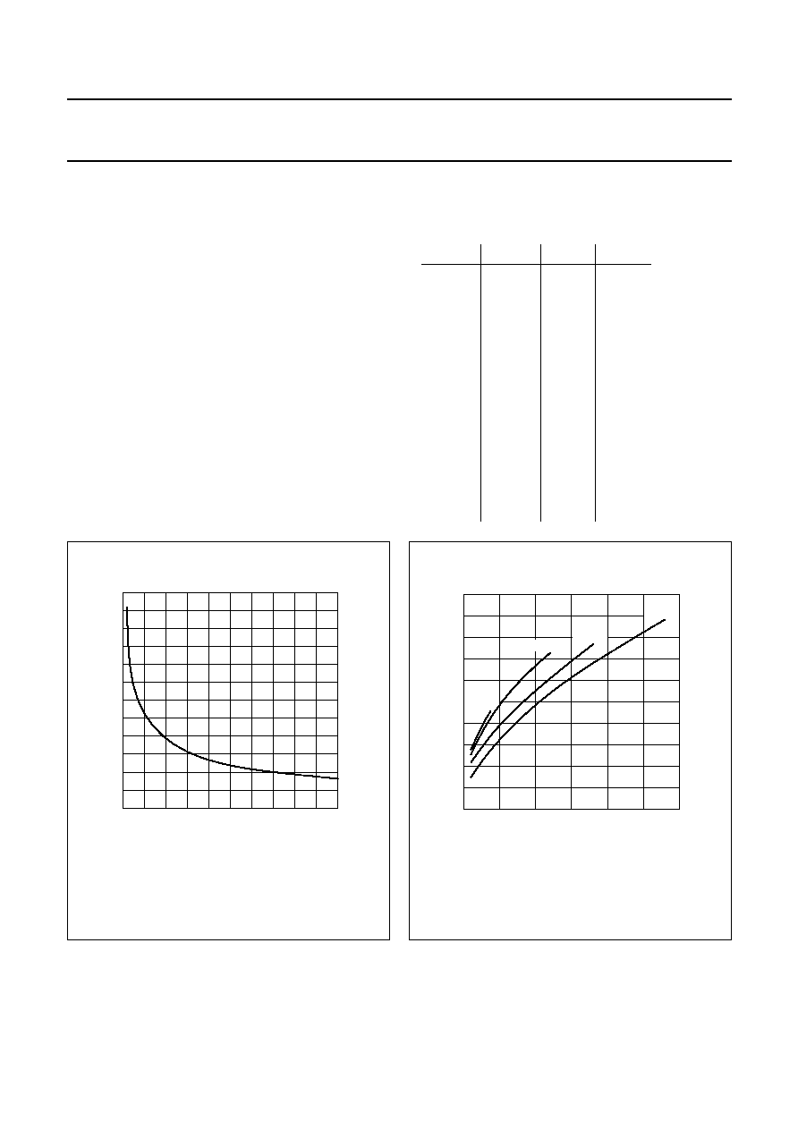
Fig.2
V
GS
= 0 for BF410A and BF410B;
I
D
= 5 mA for BF410C and BF410D;
f = 1 MHz; T
amb
= 25
�
C.
handbook, halfpage
0
typ
20
1.5
0
0.5
1
Crs
(pF)
VDS (V)
4
8
12
16
MDA277
Fig.3 V
DS
10 V; f = 1 kHz; T
amb
= 25
�
C; typical values.
handbook, halfpage
0
5
|
yfs
|
(mA/V)
ID (mA)
10
15
10
0
8
6
4
2
MDA278
BF410B
BF410A
BF410C
BF410D
December 1990
5
Philips Semiconductors
Product specification
N-channel silicon field-effect transistors
BF410A to D
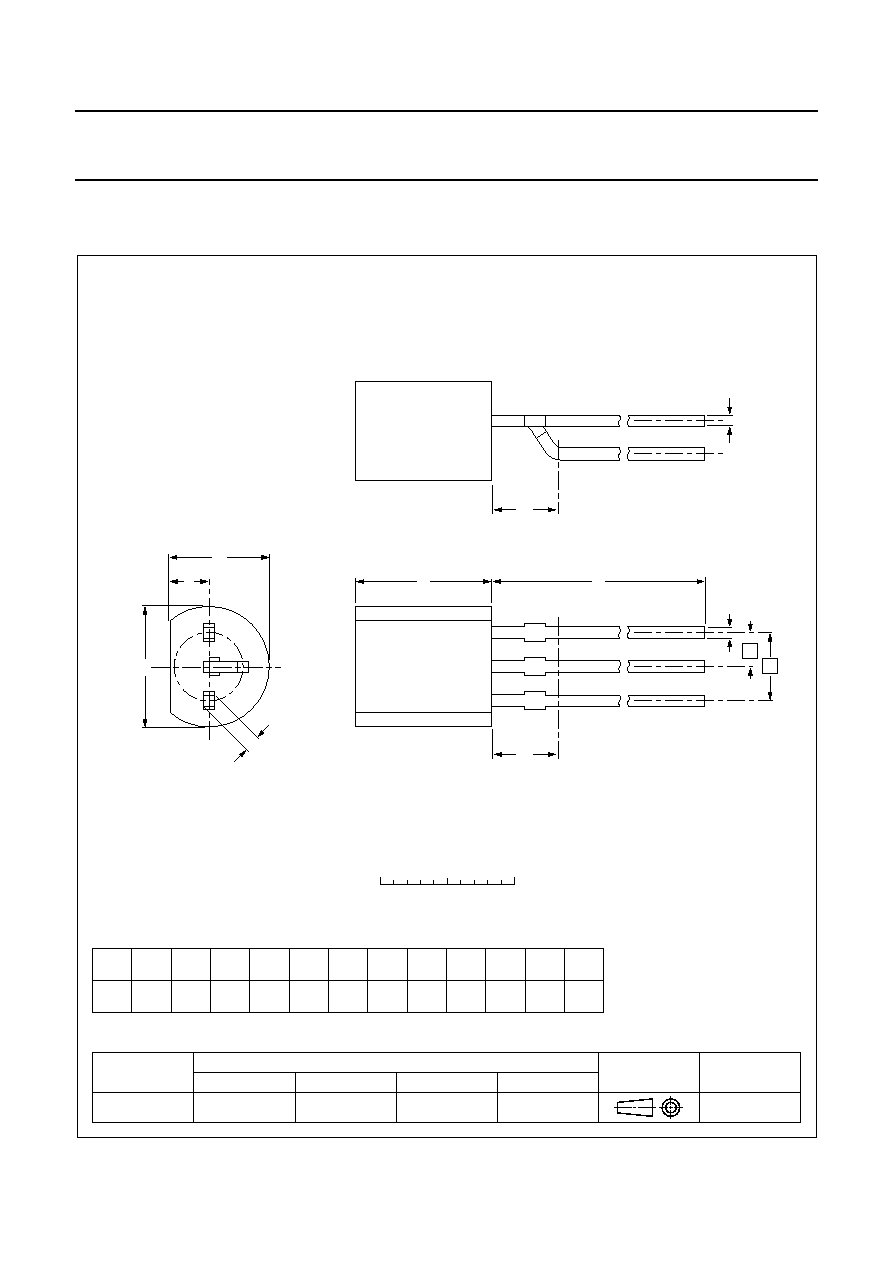
PACKAGE OUTLINE
UNIT
A
REFERENCES
OUTLINE
VERSION
EUROPEAN
PROJECTION
ISSUE DATE
IEC
JEDEC
EIAJ
mm
5.2
5.0
b
0.48
0.40
c
0.45
0.40
D
4.8
4.4
d
1.7
1.4
E
4.2
3.6
L
14.5
12.7
e
2.54
e1
1.27
L1
(1)
max
L2
max
2.5
2.5
b1
0.66
0.56
DIMENSIONS (mm are the original dimensions)
Notes
1. Terminal dimensions within this zone are uncontrolled to allow for flow of plastic and terminal irregularities.
SOT54 variant
TO-92
SC-43
A
L
0
2.5
5 mm
scale
b
c
D
b
1
L1
d
E
Plastic single-ended leaded (through hole) package; 3 leads (on-circle)
SOT54 variant
1
2
3
L2
e1
e
97-04-14