 | –≠–ª–µ–∫—Ç—Ä–æ–Ω–Ω—ã–π –∫–æ–º–ø–æ–Ω–µ–Ω—Ç: BF419 | –°–∫–∞—á–∞—Ç—å:  PDF PDF  ZIP ZIP |
DATA SHEET
Product specification
Supersedes data of September 1994
File under Discrete Semiconductors, SC04
1997 Apr 09
DISCRETE SEMICONDUCTORS
BF419
NPN high-voltage transistor
book, halfpage
M3D100
1997 Apr 09
2
Philips Semiconductors
Product specification
NPN high-voltage transistor
BF419
FEATURES
∑
Low current (max. 100 mA)
∑
High voltage (max. 250 V).
APPLICATIONS
∑
Driver for line output transistors in colour television
receivers.
DESCRIPTION
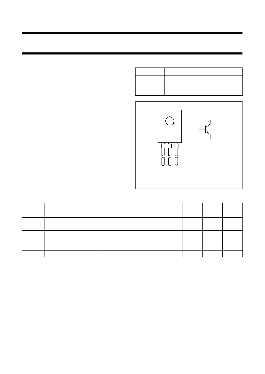
NPN high-voltage transistor in a TO-126; SOT32 plastic
package.
PINNING
PIN
DESCRIPTION
1
emitter
2
collector connected to mounting base
3
base
Fig.1
Simplified outline (TO-126; SOT32)
and symbol.
handbook, halfpage
MAM254
1
2
3
Top view
1
2
3
QUICK REFERENCE DATA
SYMBOL
PARAMETER
CONDITIONS
TYP.
MAX.
UNIT
V
CBO
collector-base voltage
open emitter
-
300
V
V
CEO
collector-emitter voltage
open base
-
250
V
I
CM
peak collector current
-
300
mA
P
tot
total power dissipation
T
mb
90
∞
C
-
6
W
h
FE
DC current gain
I
C
= 20 mA; V
CE
= 10 V
45
-
C
re
feedback capacitance
I
C
= i
c
= 0; V
CE
= 30 V; f = 1 MHz
-
3.5
pF
f
T
transition frequency
I
C
= 15 mA; V
CE
= 10 V; f = 100 MHz
90
-
MHz

1997 Apr 09
3
Philips Semiconductors
Product specification
NPN high-voltage transistor
BF419
LIMITING VALUES
In accordance with the Absolute Maximum Rating System (IEC 134).
Note
1. Precautions should be taken during switch-on of the BF419 where an overshoot of current is likely to occur.
The amplitude of the overshoot depends on the relative magnitude of stray external capacities to the transistor
collector capacity. It is desirable to keep the stray capacities to a minimum by short lead lengths etc. so as to minimize
the area of the switching path.
THERMAL CHARACTERISTICS
CHARACTERISTICS
T
j
= 25
∞
C unless otherwise specified.
Note
1. Pulse test: t
p
300
µ
s;
0.02.
SYMBOL
PARAMETER
CONDITIONS
MIN.
MAX.
UNIT
V
CBO
collector-base voltage
open emitter
-
300
V
V
CEO
collector-emitter voltage
open base
-
250
V
V
EBO
emitter-base voltage
open collector
-
5
V
I
C
collector current (DC)
-
100
mA
I
CM
peak collector current
note 1
-
300
mA
I
BM
peak base current
-
100
mA
P
tot
total power dissipation
T
mb
90
∞
C
-
6
W
T
amb
70
∞
C
-
800
mW
T
stg
storage temperature
-
65
+150
∞
C
T
j
junction temperature
-
150
∞
C
T
amb
operating ambient temperature
-
65
+150
∞
C
SYMBOL
PARAMETER
VALUE
UNIT
R
th j-a
thermal resistance from junction to ambient
100
K/W
R
th j-mb
thermal resistance from junction to mounting base
10
K/W
SYMBOL
PARAMETER
CONDITIONS
TYP.
MAX.
UNIT
I
CBO
collector cut-off current
I
E
= 0; V
CB
= 250 V
-
50
nA
I
EBO
emitter cut-off current
I
C
= 0; V
EB
= 3 V
-
50
nA
h
FE
DC current gain
I
C
= 20 mA; V
CE
= 10 V
45
-
V
CEsat
collector-emitter saturation voltage
I
C
= 200 mA; I
B
= 20 mA; note 1
-
6
V
C
c
collector capacitance
I
E
= i
e
= 0; V
CB
= 30 V; f = 1 MHz
-
4.5
pF
C
re
feedback capacitance
I
C
= i
c
= 0; V
CE
= 30 V; f = 1 MHz
-
3.5
pF
f
T
transition frequency
I
C
= 15 mA; V
CE
= 10 V; f = 100 MHz
90
-
MHz
1997 Apr 09
4
Philips Semiconductors
Product specification
NPN high-voltage transistor
BF419
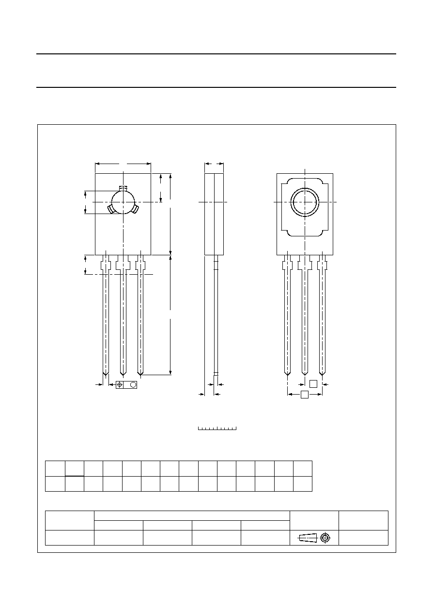
PACKAGE OUTLINE
UNIT
b
p
c
D
E
e1
L
Q
w
REFERENCES
OUTLINE
VERSION
EUROPEAN
PROJECTION
ISSUE DATE
IEC
JEDEC
EIAJ
mm
0.88
0.65
2.7
2.3
0.60
0.45
11.1
10.5
7.8
7.2
2.29
e
4.58
0.254
P
3.2
3.0
P1
3.9
3.6
DIMENSIONS (mm are the original dimensions)
Note
1. Terminal dimensions within this zone are uncontrolled to allow for flow of plastic and terminal irregularities.
16.5
15.3
1.5
0.9
L1
(1)
max
2.54
SOT32
TO-126
97-03-04
0
2.5
5 mm
scale
A
Plastic single-ended leaded (through hole) package; mountable to heatsink, 1 mounting hole; 3 leads
SOT32
D
P1
P
E
e1
A
L
Q
c
1
2
3
L1
w
M
e

1997 Apr 09
5
Philips Semiconductors
Product specification
NPN high-voltage transistor
BF419
DEFINITIONS
LIFE SUPPORT APPLICATIONS
These products are not designed for use in life support appliances, devices, or systems where malfunction of these
products can reasonably be expected to result in personal injury. Philips customers using or selling these products for
use in such applications do so at their own risk and agree to fully indemnify Philips for any damages resulting from such
improper use or sale.
Data sheet status
Objective specification
This data sheet contains target or goal specifications for product development.
Preliminary specification
This data sheet contains preliminary data; supplementary data may be published later.
Product specification
This data sheet contains final product specifications.
Limiting values
Limiting values given are in accordance with the Absolute Maximum Rating System (IEC 134). Stress above one or
more of the limiting values may cause permanent damage to the device. These are stress ratings only and operation
of the device at these or at any other conditions above those given in the Characteristics sections of the specification
is not implied. Exposure to limiting values for extended periods may affect device reliability.
Application information
Where application information is given, it is advisory and does not form part of the specification.