DATA SHEET
Product specification
File under Discrete Semiconductors, SC07
December 1997
DISCRETE SEMICONDUCTORS
BFT46
N-channel silicon FET

December 1997
2
Philips Semiconductors
Product specification
N-channel silicon FET
BFT46
DESCRIPTION
Symmetrical n-channel silicon
epitaxial planar junction field-effect
transistor in a microminiature plastic
envelope. The transistor is intended
for low level general purpose
amplifiers in thick and thin-film
circuits.
PINNING
Note : Drain and source are
interchangeable.
1 = drain
2 = source
3 = gate
Marking code
BFT46 = M3p
Fig.1 Simplified outline and symbol, SOT23.
handbook, halfpage
1
2
g
d
s
3
Top view
MAM385
QUICK REFERENCE DATA
Drain-source voltage
±
V
DS
max.
25 V
Gate-source voltage (open drain)
-
V
GSO
max.
25 V
Total power dissipation up to T
amb
= 40
∞
C
P
tot
max.
250 mW
Drain current
V
DS
= 10 V; V
GS
= 0
I
DSS
>
0,2 mA
<
1,5 mA
Transfer admittance (common source)
I
D
= 0,2 mA; V
DS
= 10 V; f = 1 kHz
y
fs
>
0,5 mS
Equivalent noise voltage
V
DS
= 10 V; I
D
= 200
µ
A; B = 0,6 to 100 Hz
V
n
<
0,5
µ
V

December 1997
3
Philips Semiconductors
Product specification
N-channel silicon FET
BFT46
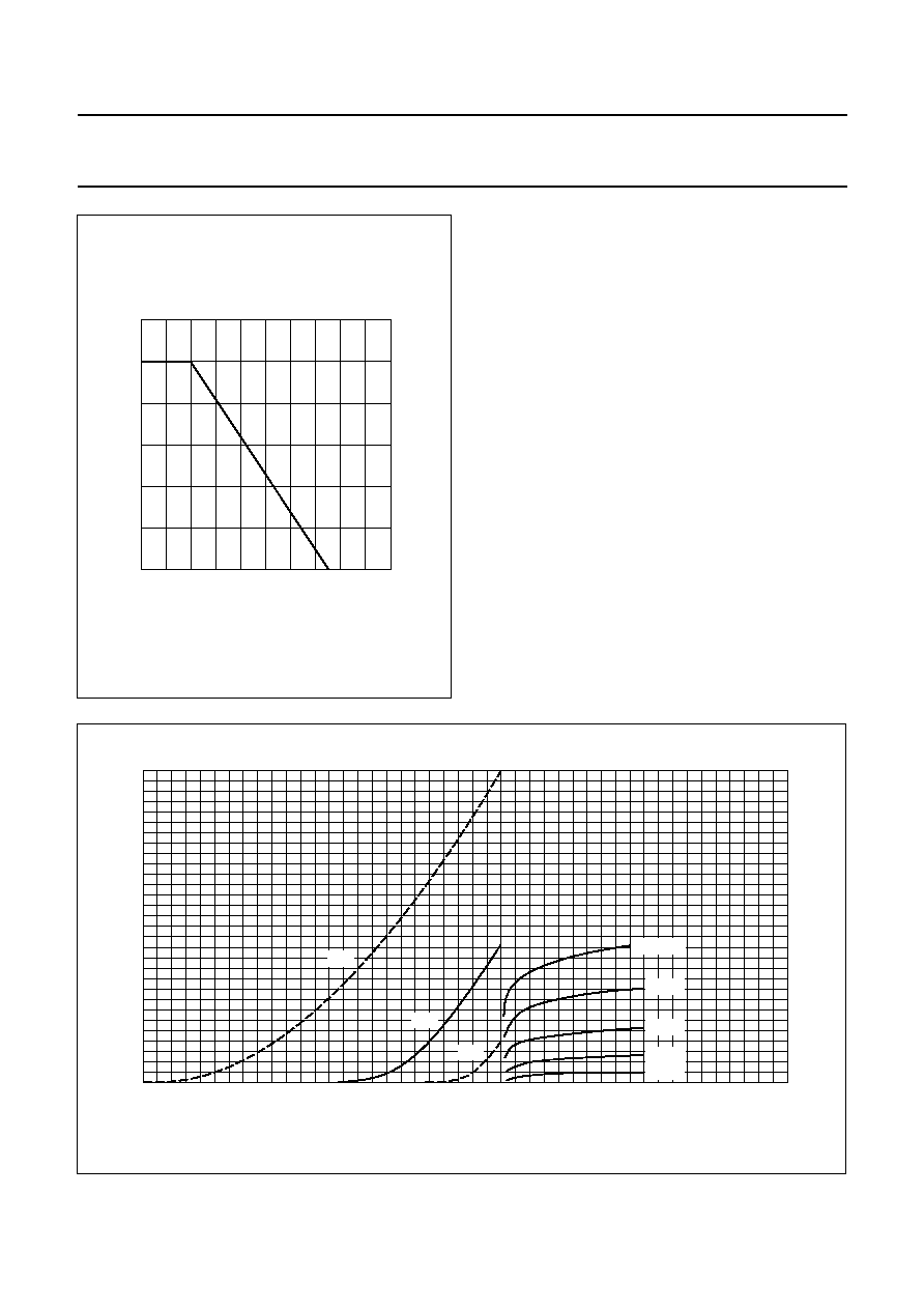
RATINGS
Limiting values in accordance with the Absolute Maximum System (IEC 134)
THERMAL RESISTANCE
Note
1. Mounted on a ceramic substrate of 8 mm
◊
10 mm
◊
0,7 mm.
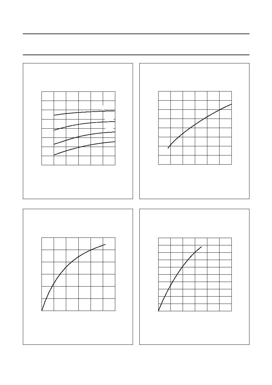
CHARACTERISTICS
T
j
= 25
∞
C unless otherwise specified
Drain-source voltage
±
V
DS
max.
25 V
Drain-gate voltage (open source)
V
DGO
max.
25 V
Gate-source voltage (open drain)
-
V
GSO
max.
25 V
Drain current
I
D
max.
10 mA
Gate current
I
G
max.
5 mA
Total power dissipation up to T
amb
= 40
∞
C
(1)
P
tot
max.
250 mW
Storage temperature range
T
stg
-
65 to
+
150
∞
C
Junction temperature
T
j
max.
150
∞
C
From junction to ambient
(1)
R
th j-a
=
430 K/W
Gate cut-off current
-
V
GS
= 10 V; V
DS
= 0
-
I
GSS
<
0,2 nA
Drain current
V
DS
= 10 V; V
GS
= 0
I
DSS
>
0,2 mA
<
1,5 mA
Gate-source voltage
I
D
= 50
µ
A; V
DS
= 10 V
-
V
GS
>
0,1 V
<
1,0 V
Gate-source cut-off voltage
I
D
= 0,5 nA; V
DS
= 10 V
-
V
(P)GS
<
1,2 V
y-parameters at f = 1 kHz;
V
DS
= 10 V; V
GS
= 0; T
amb
= 25
∞
C
Transfer admittance
y
fs
>
1,0 mS
Output admittance
y
os
<
10
µ
S
V
DS
= 10 V; I
D
= 200
µ
A; T
amb
= 25
∞
C
Transfer admittance
y
fs
>
0,5 mS
Output admittance
y
os
<
5
µ
S
Input capacitance at f = 1 MHz;
V
DS
= 10 V; V
GS
= 0; T
amb
= 25
∞
C
C
is
<
5 pF
Feedback capacitance at f = 1 MHz;
V
DS
= 10 V; V
GS
= 0; T
amb
= 25
∞
C
C
rs
<
1,5 pF
Equivalent noise voltage
V
DS
= 10 V; I
D
= 200
µ
A; T
amb
= 25
∞
C
B = 0,6 to 100 Hz
V
n
<
0,5
µ
V