 | –≠–ª–µ–∫—Ç—Ä–æ–Ω–Ω—ã–π –∫–æ–º–ø–æ–Ω–µ–Ω—Ç: BF485PN | –°–∫–∞—á–∞—Ç—å:  PDF PDF  ZIP ZIP |
Document Outline
- FEATURES
- APPLICATIONS
- DESCRIPTION
- MARKING CODE
- PINNING
- LIMITING VALUES
- THERMAL CHARACTERISTICS
- CHARACTERISTICS
- PACKAGE OUTLINE
- DATA SHEET STATUS
- DEFINITIONS
- DISCLAIMERS
DATA SHEET
Product specification
2000 Aug 02
DISCRETE SEMICONDUCTORS
BF485PN
NPN/PNP high voltage transistors
dbook, halfpage
M3D302
2000 Aug 02
2
Philips Semiconductors
Product specification
NPN/PNP high voltage transistors
BF485PN
FEATURES
∑
High voltage (max. 350 V)
∑
Low current (max. 200 mA)
∑
High power dissipation (600 mW)
∑
Two independently working transistors.
APPLICATIONS
∑
Complementary high-voltage configurations
∑
Hook switch in telephone applications.
DESCRIPTION
NPN/PNP transistors in a SOT457 (SC-74) plastic
package.
MARKING CODE
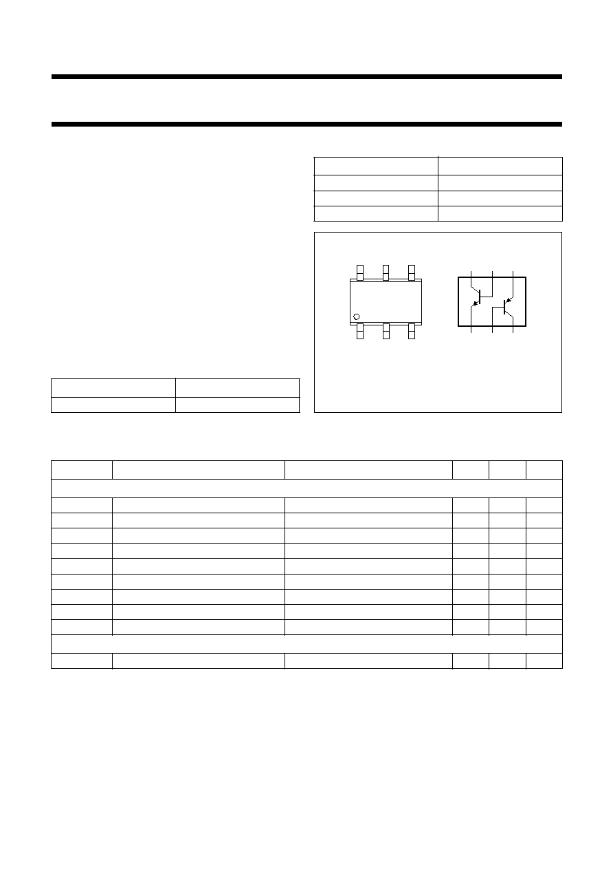
PINNING
TYPE NUMBER
CODE
BF485PN
HS
PIN
DESCRIPTION
1 and 4
emitter TR1; TR2
5 and 2
base TR1; TR2
6 and 3
collector TR1; TR2
handbook, halfpage
1
3
2
4
5
6
Top view
MAM439
1
3
2
4
5
6
TR1
TR2
Fig.1 Simplified outline (SOT457) and symbol
LIMITING VALUES
In accordance with Absolute Maximum Rating System (IEC 60134).
Note
1. Device mounted on a printed-circuit board, single-sided copper, tinplated, mounting pad for collector 1 cm
2
.
SYMBOL
PARAMETER
CONDITIONS
MIN.
MAX.
UNIT
Per transistor; for the PNP transistor with negative polarity
V
CBO
collector-base voltage
open emitter
-
350
V
V
CEO
collector-emitter voltage
open base
-
350
V
V
EBO
emitter-base voltage
open collector
-
6
V
I
O
output current (DC)
-
100
mA
I
CM
peak collector current
-
200
mA
P
tot
total power dissipation
T
amb
25
∞
C; note 1
-
600
mW
T
stg
storage temperature
-
65
+150
∞
C
T
j
junction temperature
-
150
∞
C
T
amb
operating ambient temperature range
-
65
+150
∞
C
Per device
P
tot
total power dissipation
T
amb
25
∞
C; note 1
-
300
mW
2000 Aug 02
3
Philips Semiconductors
Product specification
NPN/PNP high voltage transistors
BF485PN
THERMAL CHARACTERISTICS
Note
1. Device mounted on a printed-circuit board, single-sided copper, tinplated, mounting pad for collector 1 cm
2
.
CHARACTERISTICS
T
amb
= 25
∞
C unless otherwise specified.
SYMBOL
PARAMETER
CONDITIONS
VALUE
UNIT
R
th j-a
from junction to ambient
in free air; note 1
208
K/W
SYMBOL
PARAMETER
CONDITIONS
MIN.
MAX.
UNIT
Per transistor; for the PNP transistor with negative polarity
I
CBO
collector-base cut-off current
I
E
= 0; V
CB
= 300 V;
-
50
nA
I
E
= 0; V
CB
= 250 V; T
j
= 150
∞
C
-
50
µ
A
I
EBO
emitter-base cut-off current
I
C
= 0; V
EB
= 5 V
-
100
nA
h
FE
DC current gain
I
C
= 1 mA; V
CE
= 10 V
60
-
I
C
= 30 mA; V
CE
= 10 V
50
-
V
CEsat
saturation voltage
I
C
= 20 mA; I
B
= 2 mA
-
250
mV
V
BEsat
saturation voltage
I
C
= 20 mA; I
B
= 2 mA
-
850
mV
C
c
collector capacitance
I
E
= I
e
= 0; V
CB
= 20 V; f = 1 MHz
-
6
pF
f
T
transition frequency
I
C
= 10 mA; V
CE
= 20 V; f = 100 MHz
50
-
MHz
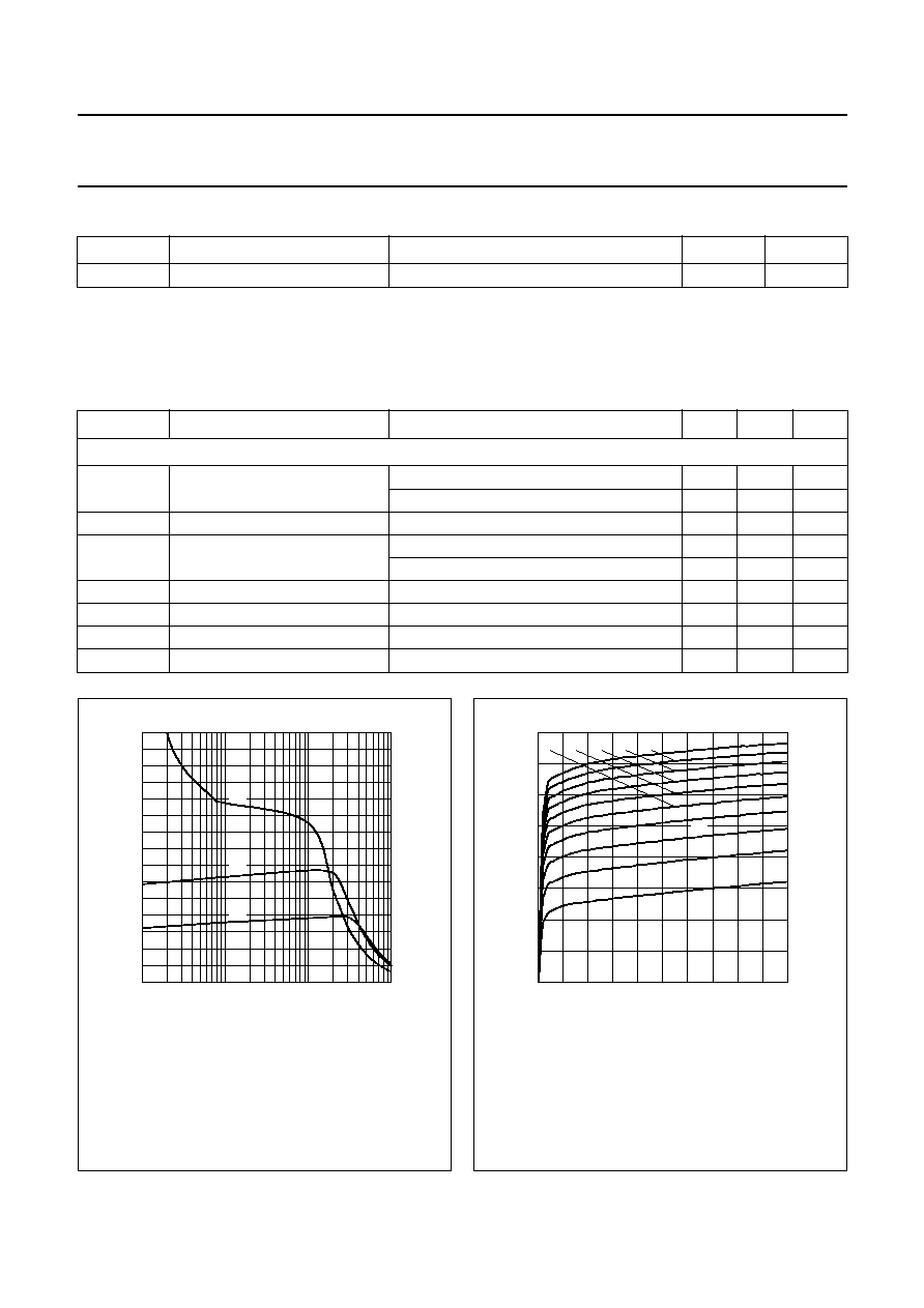
handbook, halfpage
300
0
200
100
MLD391
10
-
1
1
IC (mA)
hFE
10
10
2
(2)
(3)
(1)
Fig.2
DC current gain as a function of collector
current: typical values.
TR1 (NPN); V
CE
= 10 V.
(1) T
amb
= 150
∞
C.
(2) T
amb
= 25
∞
C.
(3) T
amb
=
-
55
∞
C.
handbook, halfpage
0
2
(1)
(6)
(7)
(10)
(2)
(3)
(4)
(5)
10
200
150
50
0
100
4
VCE (V)
IC
(mA)
6
8
MLD392
(9)
(8)
Fig.3
Collector current as a function of
collector-emitter voltage; typical values.
TR1 (NPN).
(1) I
B
= 30 mA.
(2) I
B
= 27 mA.
(3) I
B
= 24 mA.
(4) I
B
= 21 mA.
(5) I
B
= 18 mA.
(6) I
B
= 15 mA.
(7) I
B
= 12 mA.
(8) I
B
= 9 mA.
(9) I
B
= 6 mA.
(10) I
B
= 3 mA.
2000 Aug 02
4
Philips Semiconductors
Product specification
NPN/PNP high voltage transistors
BF485PN
handbook, halfpage
1000
0
10
-
1
MLD393
1
(1)
(2)
(3)
IC (mA)
VBE
(mV)
10
10
2
200
400
600
800
Fig.4
Base-emitter voltage as a function of
collector current; typical values.
TR1 (NPN); V
CE
= 10 V.
(1) T
amb
=
-
55
∞
C.
(2) T
amb
= 25
∞
C.
(3) T
amb
= 150
∞
C.
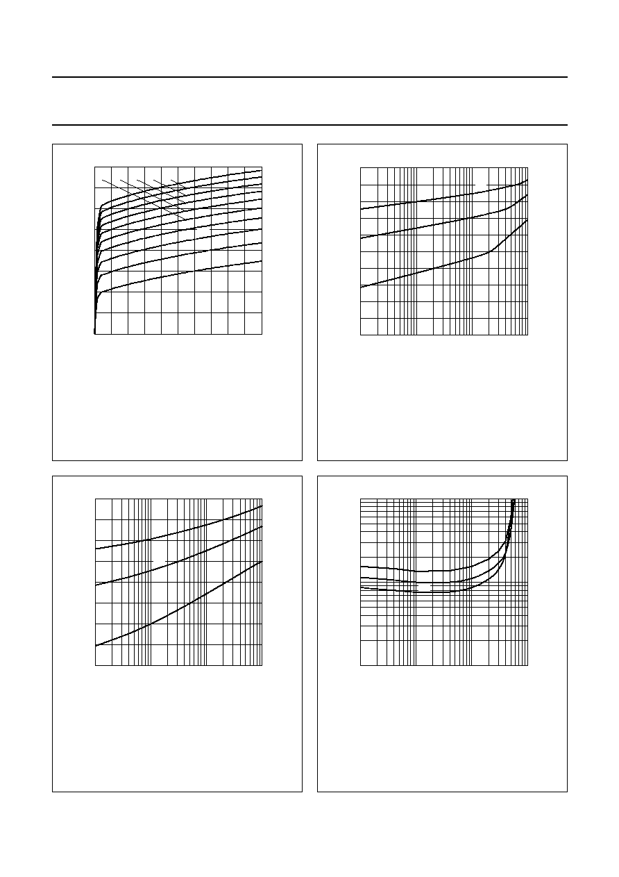
handbook, halfpage
1000
600
800
400
200
MLD394
10
-
1
1
(1)
(3)
IC (mA)
VBEsat
(mV)
10
10
2
(2)
Fig.5
Base-emitter saturation voltage as a
function of collector current.
TR1 (NPN); I
C
/I
B
= 10.
(1) T
amb
=
-
55
∞
C.
(2) T
amb
= 25
∞
C.
(3) T
amb
= 150
∞
C.
handbook, halfpage
10
3
10
2
10
MLD395
10
-
1
1
(1)
IC (mA)
VCEsat
(mV)
10
10
2
(2)
(3)
Fig.6
Collector-emitter saturation voltage as a
function of collector current: typical values.
TR1 (NPN); I
C
/I
B
= 10.
(1) T
amb
= 150
∞
C.
(2) T
amb
= 25
∞
C.
(3) T
amb
=
-
55
∞
C.
handbook, halfpage
300
0
200
100
MLD396
-
10
-
1
-
1
(1)
(2)
IC (mA)
hFE
-
10
-
10
2
(3)
Fig.7
DC current gain as a function of collector
current: typical values.
TR2 (PNP); V
CE
=
-
10 V.
(1) T
amb
= 150
∞
C.
(2) T
amb
= 25
∞
C.
(3) T
amb
=
-
55
∞
C.
2000 Aug 02
5
Philips Semiconductors
Product specification
NPN/PNP high voltage transistors
BF485PN
handbook, halfpage
0
-
2
(1)
(6)
(7)
(10)
(2)
(3)
(4)
(5)
-
10
-
200
-
150
-
50
0
-
100
-
4
VCE (V)
IC
(mA)
-
6
-
8
MLD397
(9)
(8)
Fig.8
Collector current as a function of
collector-emitter voltage; typical values.
TR2 (PNP).
(1) I
B
=
-
50 mA.
(2) I
B
=
-
45 mA.
(3) I
B
=
-
40 mA.
(4) I
B
=
-
35 mA.
(5) I
B
=
-
30 mA.
(6) I
B
=
-
25 mA.
(7) I
B
=
-
20 mA.
(8) I
B
=
-
15 mA.
(9) I
B
=
-
10 mA.
(10) I
B
=
-
5 mA.
handbook, halfpage
-
1000
0
-
10
-
1
MLD398
-
1
(2)
(3)
IC (mA)
VBE
(mV)
-
10
-
10
2
-
200
-
400
-
600
-
800
(1)
Fig.9
Base-emitter voltage as a function of
collector current; typical values.
TR2 (PNP); V
CE
=
-
10 V.
(1) T
amb
=
-
55
∞
C.
(2) T
amb
= 25
∞
C.
(3) T
amb
= 150
∞
C.
handbook, halfpage
-
1000
-
600
-
800
-
400
-
200
MLD399
-
10
-
1
-
1
(1)
(3)
IC (mA)
VBEsat
(mV)
-
10
-
10
2
(2)
Fig.10 Base-emitter saturation voltage as a
function of collector current.
TR2 (PNP); I
C
/I
B
= 10.
(1) T
amb
=
-
55
∞
C.
(2) T
amb
= 25
∞
C.
(3) T
amb
= 150
∞
C.
handbook, halfpage
-
10
3
-
10
2
-
10
MLD400
-
10
-
1
-
1
(1)
(2)
IC (mA)
VCEsat
(mV)
-
10
-
10
2
(3)
Fig.11 Collector-emitter saturation voltage as a
function of collector current: typical values.
TR2 (PNP); I
C
/I
B
= 10.
(1) T
amb
= 150
∞
C.
(2) T
amb
= 25
∞
C.
(3) T
amb
=
-
55
∞
C.