 | –≠–ª–µ–∫—Ç—Ä–æ–Ω–Ω—ã–π –∫–æ–º–ø–æ–Ω–µ–Ω—Ç: BF513 | –°–∫–∞—á–∞—Ç—å:  PDF PDF  ZIP ZIP |

DATA SHEET
Product specification
File under Discrete Semiconductors, SC07
December 1997
DISCRETE SEMICONDUCTORS
BF510 to 513
N-channel silicon field-effect
transistors
December 1997
2
Philips Semiconductors
Product specification
N-channel silicon field-effect transistors
BF510 to 513
DESCRIPTION
Asymmetrical N-channel planar
epitaxial junction field-effect
transistors in the miniature plastic
envelope intended for applications up
to the v.h.f. range in hybrid thick and
thin-film circuits. Special features are
the low feedback capacitance and the
low noise figure. These features
make the product very suitable for
applications such as the r.f. stages in
f.m. portables (BF510), car radios
(BF511) and mains radios (BF512) or
the mixer stage (BF513).
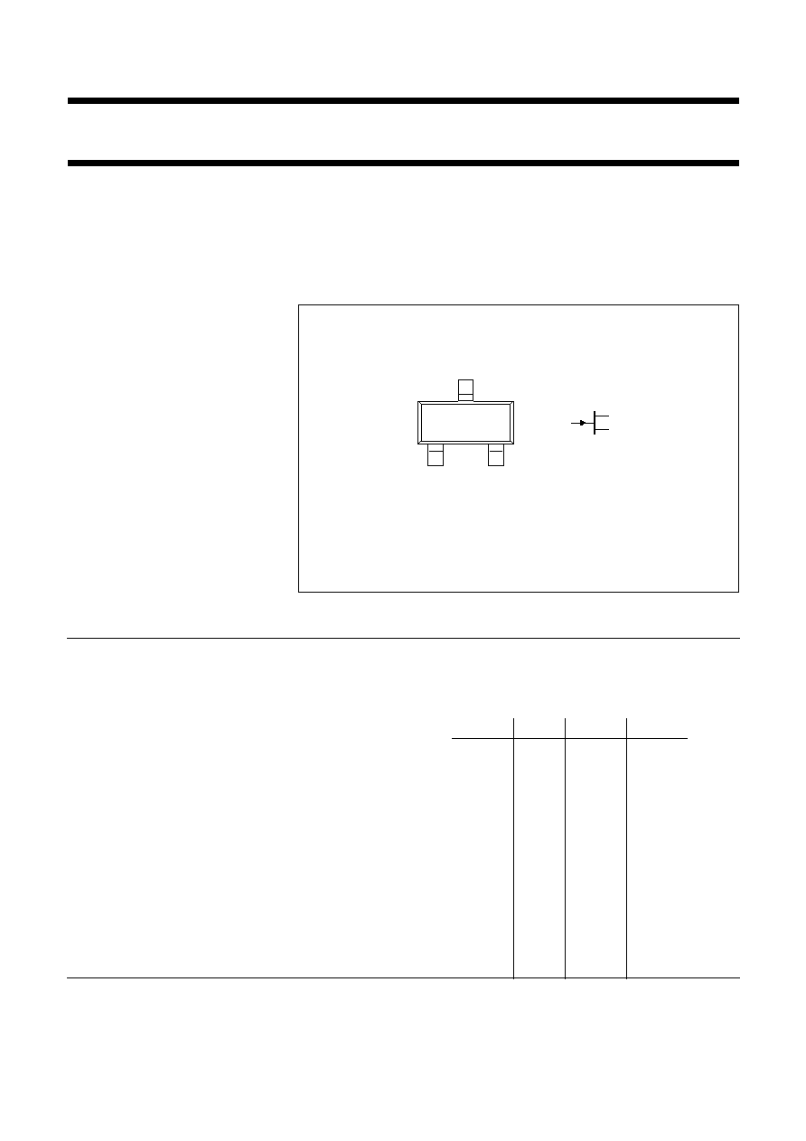
PINNING - SOT23
1
= gate
2
= drain
3
= source
MARKING CODE
BF510 = S6p
BF511 = S7p
BF512 = S8p
BF513 = S9p
Fig.1 Simplified outline and symbol.
handbook, halfpage
1
2
g
d
s
3
Top view
MAM385
QUICK REFERENCE DATA
Drain-source voltage
V
DS
max.
20
V
Drain current (DC or average)
I
D
max.
30
mA
Total power dissipation
up to T
amb
= 40
∞
C
P
tot
max.
250
mW
BF510
511
512
513
Drain current
>
0.7
2.5
6
10 mA
V
DS
= 10 V; V
GS
= 0
I
DSS
<
3.0
7.0
12
18 mA
Transfer admittance (common source)
V
DS
= 10 V; V
GS
= 0; f = 1 kHz
y
fs
>
2.5
4
6
7 mS
Feedback capacitance
V
DS
= 10 V; V
GS
= 0
C
rs
typ.
0.3
0.3
-
-
pF
V
DS
= 10 V; I
D
= 5 mA
C
rs
typ.
-
-
0.3
0.3 pF
Noise figure at optimum source admittance
G
S
= 1 mS;
-
B
S
= 3 mS; f = 100 MHz
V
DS
= 10 V; V
GS
= 0
F
typ.
1.5
1.5
-
-
dB
V
DS
= 10 V; I
D
= 5 mA
F
typ.
-
-
1.5
1.5 dB

December 1997
3
Philips Semiconductors
Product specification
N-channel silicon field-effect transistors
BF510 to 513
RATINGS
Limiting values in accordance with the Absolute Maximum System (IEC 134)
THERMAL RESISTANCE
Note
1. Mounted on a ceramic substrate of 8 mm
◊
10 mm
◊
0.7 mm.
STATIC CHARACTERISTICS
T
amb
= 25
∞
C
Drain-source voltage
V
DS
max.
20 V
Drain-gate voltage (open source)
V
DGO
max.
20 V
Drain current (DC or average)
I
D
max.
30 mA
Gate current
±
I
G
max.
10 mA
Total power dissipation up to T
amb
= 40
∞
C (note 1)
P
tot
max.
250 mW
Storage temperature range
T
stg
-
65 to
+
150
∞
C
Junction temperature
T
j
max.
150
∞
C
From junction to ambient (note 1)
R
th j-a
=
430 K/W
BF510
511
512
513
Gate cut-off current
-
V
GS
= 0.2 V; V
DS
= 0
-
I
GSS
<
10
10
10
10 nA
Gate-drain breakdown voltage
I
S
= 0;
-
I
D
= 10
µ
A
-
V
(BR)GDO
>
20
20
20
20 V
Drain current
>
<
0.7
3.0
2.5
7.0
6
12
10
18
mA
mA
V
DS
= 10 V; V
GS
= 0
I
DSS
Gate-source cut-off voltage
I
D
= 10
µ
A; V
DS
= 10 V
-
V
(P)GS
typ.
0.8
1.5
2.2
3 V
December 1997
4
Philips Semiconductors
Product specification
N-channel silicon field-effect transistors
BF510 to 513
DYNAMIC CHARACTERISTICS
Measuring conditions (common source):
V
DS
= 10 V; V
GS
= 0; T
amb
= 25
∞
C for BF510 and BF511
V
DS
= 10 V; I
D
= 5 mA; T
amb
= 25
∞
C for BF512 and BF513
y-parameters (common source)
BF510
511
512
513
Input capacitance at f = 1 MHz
C
is
<
5
5
5
5 pF
Input conductance at f = 100 MHz
g
is
typ.
100
90
60
50
µ
S
Feedback capacitance at f = 1 MHz
C
rs
typ.
0.4
0.4
0.4
0.4 pF
<
0.5
0.5
0.5
0.5 pF
Transfer admittance at f = 1 kHz
y
fs
>
2.5
4.0
4.0
3.5 mS
V
GS
= 0 instead of I
D
= 5 mA
y
fs
>
-
-
6.0
7.0 mS
Transfer admittance at f = 100 MHz
y
fs
typ.
3.5
5.5
5.0
5.0 mS
Output capacitance at f = 1 MHz
C
os
<
3
3
3
3 pF
Output conductance at f = 1 MHz
g
os
<
60
80
100
120
µ
S
Output conductance at f = 100 MHz
g
os
typ.
35
55
70
90
µ
S
Noise figure at optimum source admittance
G
S
= 1 mS;
-
B
S
= 3 mS;
f = 100 MHz
F
typ.
1.5
1.5
1.5
1.5 dB
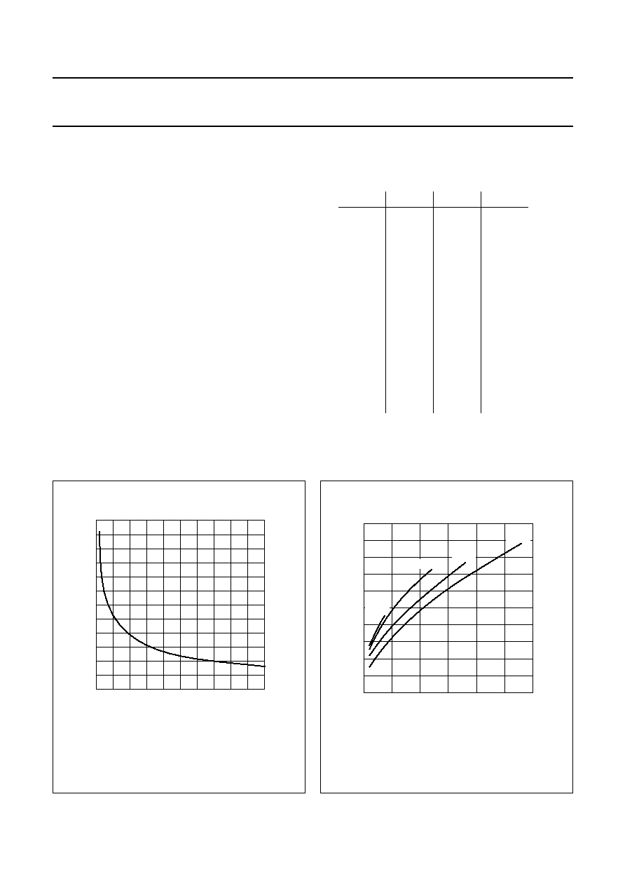
Fig.2
V
GS
= 0 for BF510 and BF511;
I
D
= 5 mA for BF512 and BF513;
f = 1 MHz; T
amb
= 25
∞
C.
handbook, halfpage
0
typ
20
1.5
0
0.5
1
Crs
(pF)
VDS (V)
4
8
12
16
MDA275
Fig.3
V
DS
= 10 V; f = 1 kHz; T
amb
= 25
∞
C; typical
values.
handbook, halfpage
0
5
|
yfs
|
(mS)
ID (mA)
10
15
10
0
8
6
4
2
MDA276
BF511
BF510
BF512
BF513
December 1997
5
Philips Semiconductors
Product specification
N-channel silicon field-effect transistors
BF510 to 513
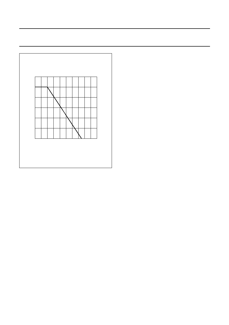
Fig.4 Power derating curve.
handbook, halfpage
0
Tamb (
∞
C)
Ptot
(mW)
300
200
100
0
40
200
80
120
160
MDA245