 | –≠–ª–µ–∫—Ç—Ä–æ–Ω–Ω—ã–π –∫–æ–º–ø–æ–Ω–µ–Ω—Ç: BF545 | –°–∫–∞—á–∞—Ç—å:  PDF PDF  ZIP ZIP |
Document Outline
- FEATURES
- APPLICATIONS
- DESCRIPTION
- PINNING - SOT23
- QUICK REFERENCE DATA
- LIMITING VALUES
- THERMAL CHARACTERISTICS
- STATIC CHARACTERISTICS
- DYNAMIC CHARACTERISTICS
- PACKAGE OUTLINE
- DEFINITIONS
- LIFE SUPPORT APPLICATIONS
DATA SHEET
Product specification
Supersedes data of April 1995
File under Discrete Semiconductors, SC07
1996 Jul 29
DISCRETE SEMICONDUCTORS
BF545A; BF545B; BF545C
N-channel silicon junction
field-effect transistors
1996 Jul 29
2
Philips Semiconductors
Product specification
N-channel silicon junction
field-effect transistors
BF545A; BF545B; BF545C
FEATURES
∑
Low leakage level (typ. 500 fA)
∑
High gain
∑
Low cut-off voltage (max. 2.2 V for BF545A).
APPLICATIONS
∑
Impedance converters in e.g. electret microphones and
infra-red detectors
∑
VHF amplifiers in oscillators and mixers.
DESCRIPTION
N-channel symmetrical silicon junction field-effect
transistors in a SOT23 package.
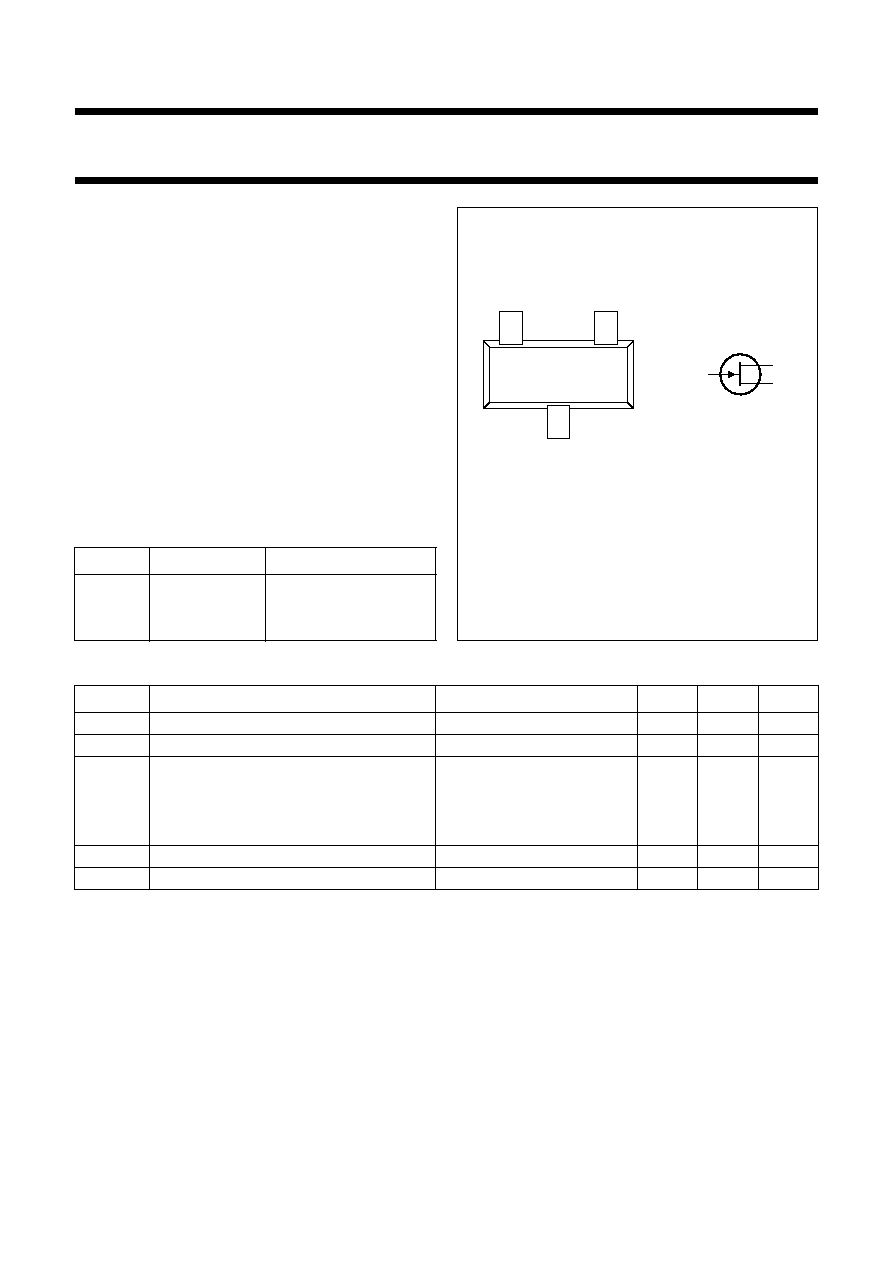
PINNING - SOT23
PIN
SYMBOL
DESCRIPTION
1
s
source
2
d
drain
3
g
gate
Fig.1 Simplified outline and symbol.
Marking codes:
BF545A: M65.
BF545B: M66.
BF545C: M67.
handbook, halfpage
s
d
g
2
1
3
MAM036
Top view
QUICK REFERENCE DATA
SYMBOL
PARAMETER
CONDITIONS
MIN.
MAX.
UNIT
V
DS
drain-source voltage
-
±
30
V
V
GSoff
gate-source cut-off voltage
I
D
= 1
µ
A; V
DS
= 15 V
-
0.4
-
7.8
V
I
DSS
drain current
V
GS
= 0; V
DS
= 15 V
BF545A
2
6.5
mA
BF545B
6
15
mA
BF545C
12
25
mA
P
tot
total power dissipation
up to T
amb
= 25
∞
C
-
250
mW
y
fs
forward transfer admittance
V
GS
= 0; V
DS
= 15 V
3
6.5
mS
1996 Jul 29
3
Philips Semiconductors
Product specification
N-channel silicon junction
field-effect transistors
BF545A; BF545B; BF545C
LIMITING VALUES
In accordance with the Absolute Maximum Rating System (IEC 134).
Note
1. Device mounted on an FR4 printed-circuit board, maximum lead length 4 mm; mounting pad for the drain
lead 10 mm
2
.
SYMBOL
PARAMETER
CONDITIONS
MIN.
MAX.
UNIT
V
DS
drain-source voltage
-
±
30
V
V
GSO
gate-source voltage
open drain
-
-
30
V
V
GDO
gate-drain voltage (DC)
open source
-
-
30
V
I
G
forward gate current (DC)
-
10
mA
P
tot
total power dissipation
up to T
amb
= 25
∞
C; note 1
-
250
mW
T
stg
storage temperature
-
65
150
∞
C
T
j
operating junction temperature
-
150
∞
C
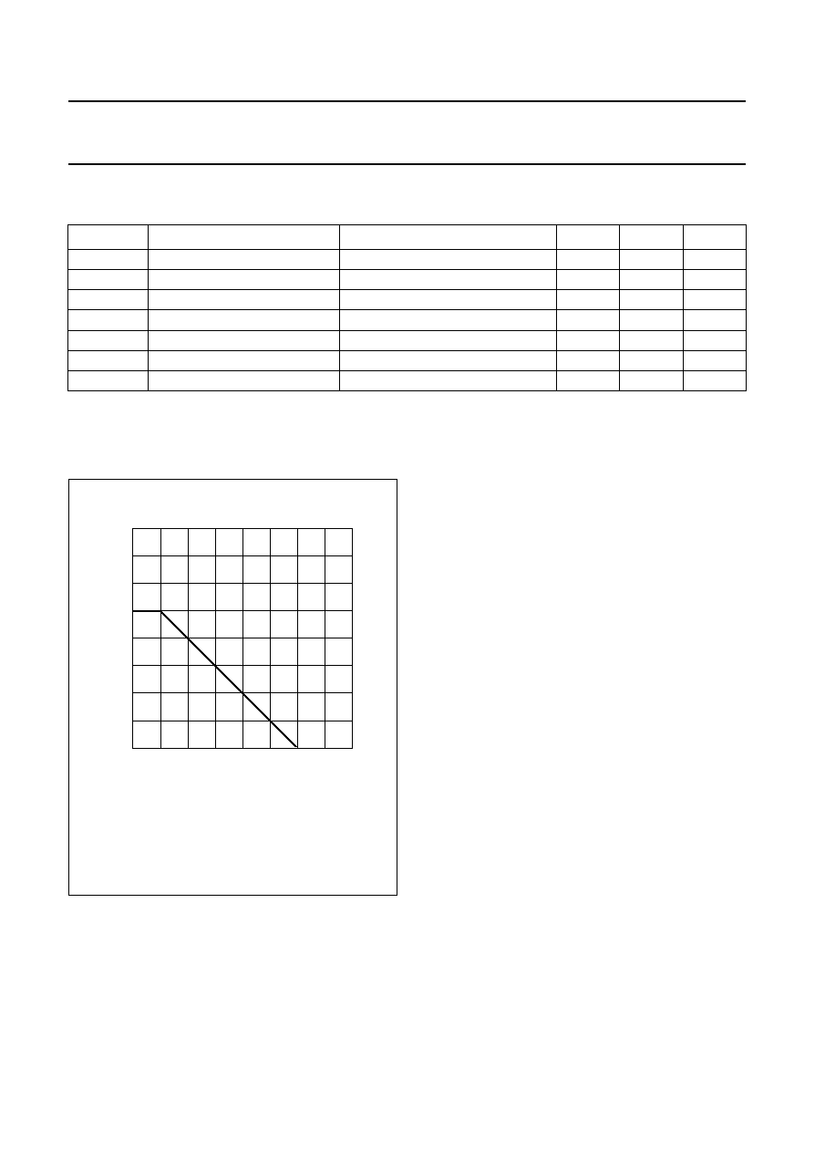
Fig.2 Power derating curve.
handbook, halfpage
0
50
100
200
400
300
100
0
200
150
MBB688
Ptot
(mW)
Tamb (
∞
C)

1996 Jul 29
4
Philips Semiconductors
Product specification
N-channel silicon junction
field-effect transistors
BF545A; BF545B; BF545C
THERMAL CHARACTERISTICS
Note
1. Device mounted on an FR4 printed-circuit board, maximum lead length 4 mm; mounting pad for the drain
lead 10 mm
2
.
STATIC CHARACTERISTICS
T
j
= 25
∞
C; unless otherwise specified.
SYMBOL
PARAMETER
VALUE
UNIT
R
th j-a
thermal resistance from junction to ambient; note 1
500
K/W
SYMBOL
PARAMETER
CONDITIONS
MIN.
TYP.
MAX.
UNIT
V
(BR)GSS
gate-source breakdown voltage I
G
=
-
1
µ
A; V
DS
= 0
-
30
-
-
V
V
GSoff
gate-source cut-off voltage
I
D
= 200
µ
A; V
DS
= 15 V
BF545A
-
0.4
-
-
2.2
V
BF545B
-
1.6
-
-
3.8
V
BF545C
-
3.2
-
-
7.8
V
I
D
= 1
µ
A; V
DS
= 15 V
-
0.4
-
-
7.5
V
I
DSS
drain current
V
GS
= 0; V
DS
= 15 V
BF545A
2
-
6.5
mA
BF545B
6
-
15
mA
BF545C
12
-
25
mA
I
GSS
gate leakage current
V
GS
=
-
20 V; V
DS
= 0
-
-
0.5
-
1000
pA
V
GS
=
-
20 V; V
DS
= 0;
T
j
= 125
∞
C
-
-
-
100
nA
y
fs
forward transfer admittance
V
GS
= 0; V
DS
= 15 V
3
-
6.5
mS
y
os
common source output
admittance
V
GS
= 0; V
DS
= 15 V
-
40
-
µ
S
1996 Jul 29
5
Philips Semiconductors
Product specification
N-channel silicon junction
field-effect transistors
BF545A; BF545B; BF545C
DYNAMIC CHARACTERISTICS
T
amb
= 25
∞
C; unless otherwise specified.
SYMBOL
PARAMETER
CONDITIONS
TYP.
UNIT
C
is
input capacitance
V
DS
= 15 V; V
GS
=
-
10 V; f = 1 MHz
1.7
pF
V
DS
= 15 V; V
GS
= 0; f = 1 MHz
3
pF
C
rs
reverse transfer capacitance
V
DS
= 15 V; V
GS
=
-
10 V; f = 1 MHz
0.8
pF
V
DS
= 15 V; V
GS
= 0; f = 1 MHz
0.9
pF
g
is
common source input conductance V
DS
= 10 V; I
D
= 1 mA; f = 100 MHz
15
µ
S
V
DS
= 10 V; I
D
= 1 mA; f = 450 MHz
300
µ
S
g
fs
common source transfer
conductance
V
DS
= 10 V; I
D
= 1 mA; f = 100 MHz
2
mS
V
DS
= 10 V; I
D
= 1 mA; f = 450 MHz
1.8
mS
g
rs
common source reverse
conductance
V
DS
= 10 V; I
D
= 1 mA; f = 100 MHz
-
6
µ
S
V
DS
= 10 V; I
D
= 1 mA; f = 450 MHz
-
40
µ
S
g
os
common source output
conductance
V
DS
= 10 V; I
D
= 1 mA; f = 100 MHz
30
µ
S
V
DS
= 10 V; I
D
= 1 mA; f = 450 MHz
60
µ
S
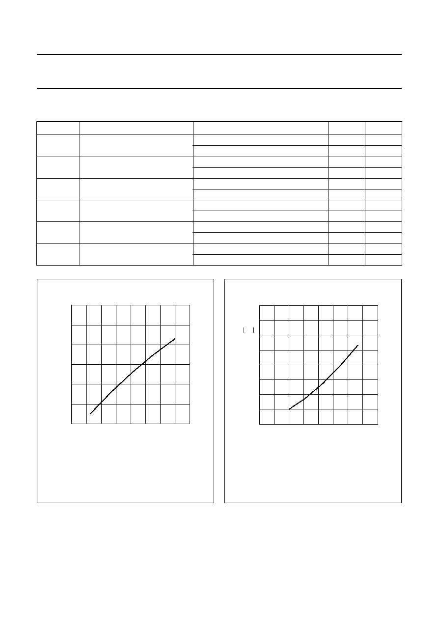
Fig.3
Drain current as a function of gate-source
cut-off voltage; typical values.
V
DS
= 15 V; T
j
= 25
∞
C.
handbook, halfpage
0
30
20
10
0
-
2
-
4
-
8
-
6
MBB467
IDSS
(mA)
VGSoff (V)
Fig.4
Forward transfer admittance as a
function of gate-source cut-off voltage;
typical values.
V
DS
= 15 V; V
GS
= 0; T
j
= 25
∞
C.
handbook, halfpage
0
6
5
4
-
2
-
4
-
8
MBB466
-
6
VGSoff (V)
Yfs
(mS)