 | –≠–ª–µ–∫—Ç—Ä–æ–Ω–Ω—ã–π –∫–æ–º–ø–æ–Ω–µ–Ω—Ç: BF585 | –°–∫–∞—á–∞—Ç—å:  PDF PDF  ZIP ZIP |
DATA SHEET
Product specification
Supersedes data of September 1994
File under Discrete Semiconductors, SC04
1996 Dec 09
DISCRETE SEMICONDUCTORS
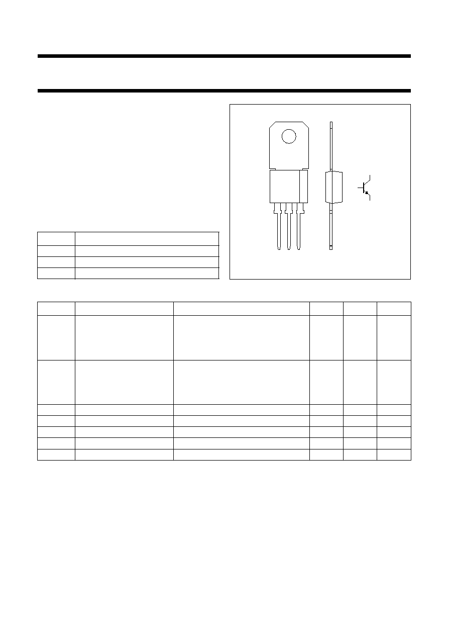
BF583; BF585; BF587
NPN high-voltage transistors
M3D067
1996 Dec 09
2
Philips Semiconductors
Product specification
NPN high-voltage transistors
BF583; BF585; BF587
FEATURES
∑
Low feedback capacitance.
APPLICATIONS
∑
For use in video output stages of black and white and
colour television receivers.
DESCRIPTION
NPN transistors in a TO-202 plastic package.
PINNING
PIN
DESCRIPTION
1
emitter
2
collector
3
base
Fig.1
Simplified outline (TO-202) and symbol.
handbook, halfpage
1
2
3
MBH793
2
3
1
QUICK REFERENCE DATA
SYMBOL
PARAMETER
CONDITIONS
MIN.
MAX.
UNIT
V
CBO
collector-base voltage
open emitter
BF583
-
300
V
BF585
-
350
V
BF587
-
400
V
V
CEO
collector-emitter voltage
open base
BF583
-
250
V
BF585
-
300
V
BF587
-
350
V
I
CM
peak collector current
-
100
mA
P
tot
total power dissipation
in free air; T
amb
25
∞
C
-
1.6
W
h
FE
DC current gain
I
C
= 25 mA; V
CE
= 20 V
-
50
C
re
feedback capacitance
I
C
= i
c
= 0; V
CE
= 30 V; f = 1 MHz
-
1.8
pF
f
T
transition frequency
I
C
= 10 mA; V
CE
= 10 V
70
110
MHz
1996 Dec 09
3
Philips Semiconductors
Product specification
NPN high-voltage transistors
BF583; BF585; BF587
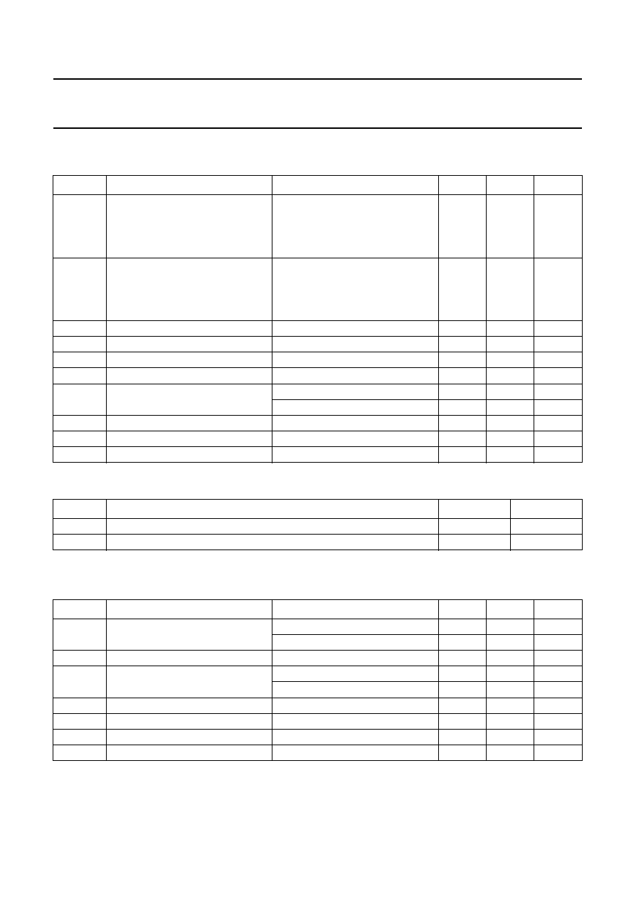
LIMITING VALUES
In accordance with the Absolute Maximum Rating System (IEC 134).
THERMAL CHARACTERISTICS
CHARACTERISTICS
T
j
= 25
∞
C unless otherwise specified.
SYMBOL
PARAMETER
CONDITIONS
MIN.
MAX.
UNIT
V
CBO
collector-base voltage
open emitter
BF583
-
300
V
BF585
-
350
V
BF587
-
400
V
V
CEO
collector-emitter voltage
open base
BF583
-
250
V
BF585
-
300
V
BF587
-
350
V
V
EBO
emitter-base voltage
open collector
-
5
V
I
C
collector current (DC)
50
-
mA
I
CM
peak collector current
-
100
mA
I
BM
peak base current
-
50
mA
P
tot
total power dissipation
in free air; T
amb
25
∞
C
-
1.6
W
in free air; T
mb
25
∞
C
-
5
W
T
stg
storage temperature
-
65
+150
∞
C
T
j
junction temperature
-
150
∞
C
T
amb
operating ambient temperature
-
65
+150
∞
C
SYMBOL
PARAMETER
VALUE
UNIT
R
th j-a
thermal resistance from junction to ambient
78
K/W
R
th j-mb
thermal resistance from junction to mounting base
25
K/W
SYMBOL
PARAMETER
CONDITIONS
MIN.
MAX.
UNIT
I
CBO
collector cut-off current
I
E
= 0; V
CB
= 300 V
-
20
nA
I
E
= 0; V
CB
= 250 V; T
j
= 150
∞
C
-
20
µ
A
I
EBO
emitter cut-off current
I
C
= 0; V
EB
= 5 V
-
100
nA
h
FE
DC current gain
I
C
= 25 mA; V
CE
= 20 V
50
-
I
C
= 40 mA; V
CE
= 20 V
20
-
V
CEsat
collector-emitter saturation voltage
I
C
= 30 mA; I
B
= 5 mA
-
600
mV
C
c
collector capacitance
I
E
= i
e
= 0; V
CB
= 30 V; f = 1 MHz
-
2.5
pF
C
re
feedback capacitance
I
C
= i
c
= 0; V
CE
= 30 V; f = 1 MHz
-
1.8
pF
f
T
transition frequency
I
C
= 10 mA; V
CE
= 10 V
70
110
MHz
1996 Dec 09
4
Philips Semiconductors
Product specification
NPN high-voltage transistors
BF583; BF585; BF587
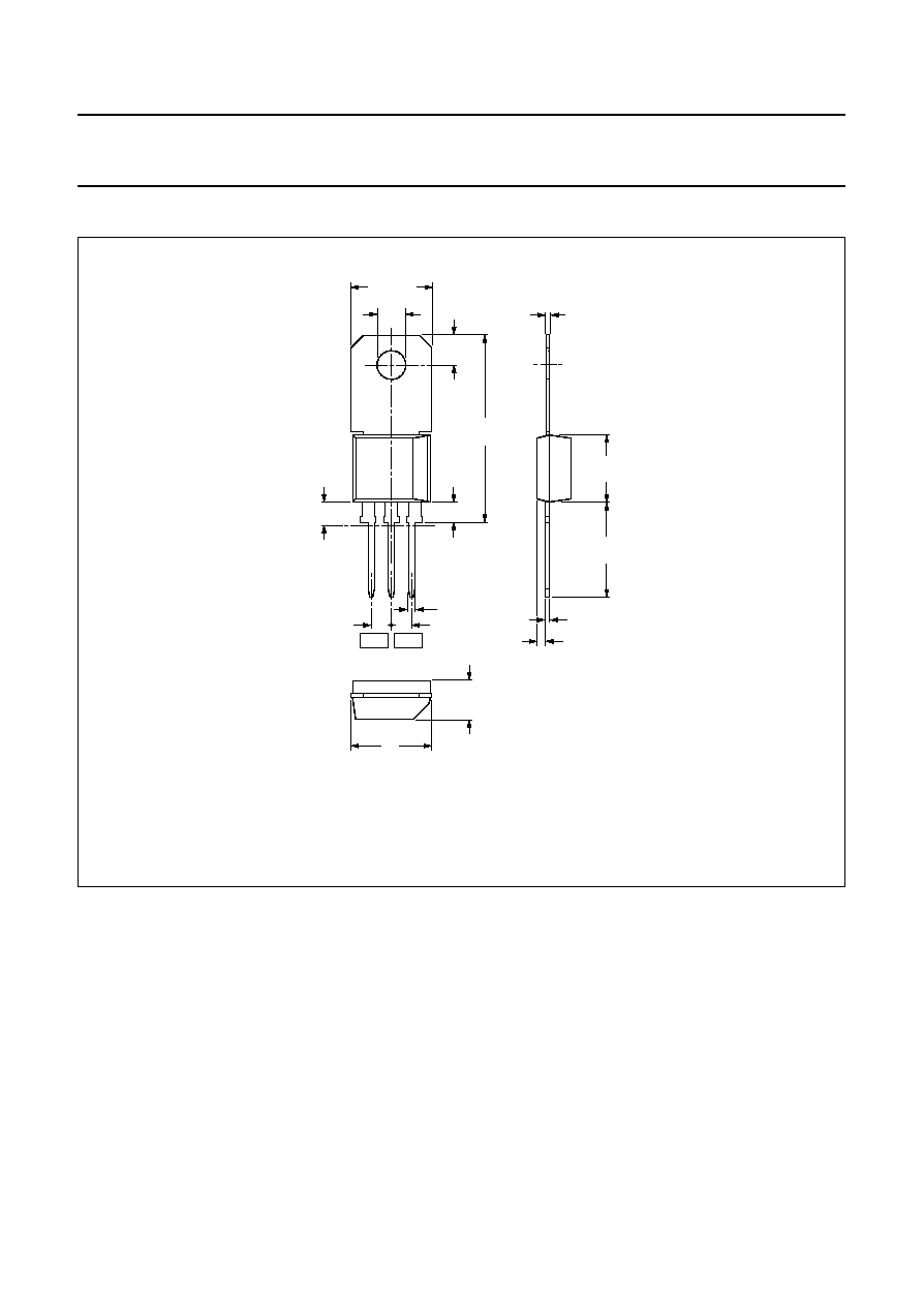
PACKAGE OUTLINE
Fig.2 TO-202.
Dimensions in mm.
(1) Terminal dimensions within this zone are uncontrolled.
handbook, full pagewidth
10.4 max
3.8
3.6
12.2
min
10
1
2
3
8.6
max
4.6
max
0.8 (3x)
2.54
2.54
2.5 max
(1)
2.4 max
3.8
24.2
max
0.65 max
0.56 max
1.6
0.6
MGA322

1996 Dec 09
5
Philips Semiconductors
Product specification
NPN high-voltage transistors
BF583; BF585; BF587
DEFINITIONS
LIFE SUPPORT APPLICATIONS
These products are not designed for use in life support appliances, devices, or systems where malfunction of these
products can reasonably be expected to result in personal injury. Philips customers using or selling these products for
use in such applications do so at their own risk and agree to fully indemnify Philips for any damages resulting from such
improper use or sale.
Data sheet status
Objective specification
This data sheet contains target or goal specifications for product development.
Preliminary specification
This data sheet contains preliminary data; supplementary data may be published later.
Product specification
This data sheet contains final product specifications.
Limiting values
Limiting values given are in accordance with the Absolute Maximum Rating System (IEC 134). Stress above one or
more of the limiting values may cause permanent damage to the device. These are stress ratings only and operation
of the device at these or at any other conditions above those given in the Characteristics sections of the specification
is not implied. Exposure to limiting values for extended periods may affect device reliability.
Application information
Where application information is given, it is advisory and does not form part of the specification.